No-Clean Flux Residue and Underfill Compatibility Effects on Electrical Reliability
|
|
|
- Frederica Snow
- 6 years ago
- Views:
Transcription
1 No-Clean Flux Residue and Underfill Compatibility Effects on Electrical Reliability Eric Bastow Indium Corporation Utica, NY No-clean soldering processes dominate the commercial electronics manufacturing world. With the explosion of growth in handheld electronics devices, manufacturers have been forced to look for ways to reinforce their assemblies against the inevitable bumps and drops that their products experience in the field. One method of reinforcement has been the utilization of underfills to glue certain surface mount devices (SMDs) to the PCB. This provides additional mechanical strength over and above the soldered connections. Bumped SMDs attached to the PCB with a no-clean soldering process offer the unavoidable scenario of the underfill coming in contact with a flux residue. This may or may not create a reliability issue. No-clean solder paste flux chemistries can vary. Some have halogens and others do not. Some have standard residues and others have residues optimized for pin probing. There are also a number of underfill chemistries on the market. Furthermore, underfill curing conditions vary depending on whether the SMDs are exposed on the surface of the PCB or underneath an RF shield. This paper will discuss an experiment designed to measure the electrical reliability of various combinations of underfill and no-clean flux residues, as measured with J-STD-004B SIR (IPC-TM ). Procedural Backgroup and Set-Up For the experiment, a matrix of three different Pb-Free, no-clean solder pastes and four different underfills were used. The individual materials (solder pastes and underfills) were tested by themselves, as well, in order to establish the baseline performance for each. The solder pastes are described as the following: 1) Halogen-containing with a standard residue 2) Halogen-free with a standard residue 3) Halogen-free with a residue optimized for pin-probing Note: All pastes contained the SAC305 alloy (96.5%Sn 3.0%Ag 0.5%Cu) The four underfills are described by the respective manufacturers as follows: 1) Underfill A is a reworkable underfill encapsulant for CSP and BGA encapsulation that cures quickly at low temperature. It is capable of flowing quickly across distances of 750 mils and greater. This encapsulant exhibits excellent adhesion to organic substrates. 2) Underfill B - is a reworkable underfill encapsulant for CSP and BGA encapsulation that cures quickly at low temperature. It is capable of flowing quickly across distances of 750 mils and greater. This encapsulant exhibits excellent adhesion to organic substrates. 3) Underfill C - is a reworkable underfill encapsulant for CSP and BGA encapsulation that cures quickly at low temperature. It is capable of flowing quickly across distances of 750 mils and greater. This encapsulant exhibits excellent adhesion to organic substrates. 4) Underfill D reworkable epoxy underfill is designed for CSP and BGA applications. It cures quickly at moderate temperatures to minimize stress to other components, and when cured provides excellent mechanical stress protection for solder joints. Note: The author s company does not manufacture underfills. These underfills were sourced from two world class underfill manufacturers and the individual chemistries were selected for this experiment based upon their popularity. Since the experiment seeks to measure the compatibility of the no-clean solder pastes residues and underfills based on surface insulation resistance (SIR) performance, the IPC-B-24 SIR test coupon was used as the test vehicle. Each test coupon contains four SIR patterns. Two IPC-B-24 SIR test coupons (a total of eight SIR patterns) were prepared and tested for each individual material and solder paste/underfill combination. Furthermore, an additional objective of understanding what impact entrapment under an RF shield has on the SIR performance of such combinations was incorporated into the experiment. Two SIR patterns, patterns B and D, on each IPC- B-24 SIR test coupon were covered with RF shields. Every IPC-B-24 SIR test coupon, whether using solder paste alone, underfill alone, or a solder paste/underfill combination, was prepared with the RF shields affixed in place - both during solder
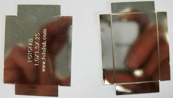
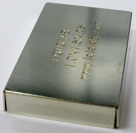
2 paste reflow and underfill curing. The RF shields were cleaned with isopropyl alcohol before being used. Figures 1 and 2 are photographs of the RF shields that were used. Figure 1 - Unfolded RF Shield Figure 2 - Folded RF Shield The following photograph (Figure 3) shows the location of the RF shields and thermocouples as used for establishing the solder paste reflow profile and underfill cure profiles.
3 Figure 3 - IPC-B-24 SIR Test Coupon showing location of thermocouples and RF shields Figure 4 shows the profile used to reflow the three solder pastes. The thermocouples, identified in the reflow profile as TC 2 and TC 5, were located on the SIR patterns under the RF shields. Those identified as TC 3 and TC 4 were located on the exposed SIR patterns. The exposed SIR patterns achieved a peak temperature of ~249 C and the SIR patterns covered with the RF shields achieved a peak temperature of ~244 C. Figure 4 - Solder Paste Reflow Profile
4 The following were the manufacturer recommended cure cycles for the respective underfills: 1) Underfill A 165 C for 5 minutes 2) Underfill B 150 C for 1 to 6 minutes 3) Underfill C 150 C for 3 to 6 minutes 4) Underfill D 130 C for 8 minutes Figures 5, 6, and 7 show the underfill cure profiles that were obtained using a set-up similar to what is depicted in Figure 3. For underfills B and C, the same cure profile was used (Figure 6). No care was taken to identify which thermocouples were located under the RF shields and which were located on the exposed SIR patterns. Presumably the patterns under the RF shields would have achieved a slightly lower peak temperature than those located on the exposed SIR patterns. Figure 5 - Cure Profile used for Underfill A Figure 6 - Cure Profile used for Underfills B and C
5 Figure 7 - Cure Profile used for Underfill D Procedure For the two SIR test coupons prepared for each solder paste, the paste was stencil printed onto the test coupons using a stencil that is in accordance with the IPC prescribed stencil parameters. Then an RF shield was affixed over patterns B and D on each of the two SIR test coupons (see Figure 8). The SIR test coupons were then submitted to the reflow profile depicted in Figure 4. Figure 9 shows the SIR test coupon after it was reflowed. Figure 10 shows the reflowed SIR test coupon with the RF shields removed. Figure 8 - SIR Test Coupon Showing Printed Paste and RF Shields Affixed Over Patterns B and D
.")
.")
6 Figure 9 - Pasted SIR Test Coupon after Reflow Figure 10 - Pasted and Reflowed SIR Test Coupon with RF Shields Removed For the two SIR test coupons prepared for each underfill, the underfill was dispensed onto the test coupons (see Figure 11). The underfill was then mechanically moved around to cover the entire SIR pattern with a razor blade (see Figure 12). Next, an RF shield was affixed over patterns B and D on each of the two SIR test coupons (see Figure 13). The SIR test coupons were then submitted to the specific cure profile as prescribed by the underfill manufacturer (Figures 5, 6, and 7). Figures 14 and 15 show the cured underfill SIR test coupons with RF shields affixed and removed, respectively.
7 Figure 11 - Dispensed Underfill on the SIR Test Coupon Figure 12 - Smeared Underfill Covering Entire SIR Pattern
8 Figure 13 - Underfill Covered SIR Test Board with RF Shields Affixed Figure 14 - Cured Underfill Test Coupon with RF Shields Affixed
9 Figure 15 - Cured Underfill SIR Test Coupon with RF Shields Removed For the two SIR test coupons prepared for each solder paste/underfill combination, the solder paste was printed and reflowed in the same manner as the SIR test coupons prepared with solder paste only. Then the RF shields were removed and underfill was applied to each SIR pattern in the same manner as the SIR test coupons prepared with underfill only. The RF shields were reaffixed to their original locations and the SIR test coupon was submitted to the appropriate underfill cure profile. Upon completion of the preparation of all the SIR test coupons (solder paste only, underfill only and solder paste/underfill combination) all RF shields were removed. The SIR test coupons were then tested per the SIR test conditions and methods as prescribed per J-STD-004B. SIR measurements were taken every 20 minutes. The SIR measurements for the four exposed SIR patterns were averaged, and the SIR measurements for the four RF shield covered SIR patterns were averaged (from the two SIR test coupons prepared for each material or combination) and graphed as a function of resistance versus time. Following are the graphs. (Given the highly resistive nature of the flux residues and underfills, taking measurements at low voltage is subject to a certain amount of system noise. From time to time upward and/or downward spikes will be observed in the graphs. In such cases, one should focus on the general trend of the graph instead of the noise.)
10 Results
11
12
13 Note: Three of the eight SIR patterns produced values below the IPC required minimum value of 1x10^8 ohms per square. The effect of averaging makes the plotted lines stay higher.
14
15
16
17 Note: One of the eight SIR patterns produced values below the IPC required minimum value of 1x10^8 ohms per square. The effect of averaging makes the plotted line stay higher.
18
19
20 Observations and Conclusions It was observed that Underfill B produced a unique visual anomaly as can be seen in Figure 16. This anomaly was especially pronounced on the SIR patterns that were covered with RF shields. It is not known whether the underfill looked this way after curing or not until after SIR testing. None of the other underfills exhibited this sort of phenomenon. Figure 16 - Anomaly in Underfill B, Post SIR Testing (RF Shield Pattern)
21 In a previous work, the author studied the impact of RF shields on no-clean flux residues. In that work, the results showed that entrapping a flux residue under an RF shield consistently produced lower SIR results than residues that were fully exposed (not covered). In that work, the RF shields were larger, produced a better seal (restricted outgassing), noticeably reduced the peak temperature of the SIR patterns below the shields, and were left on the patterns during SIR testing. In this study, certain materials and combinations, especially the underfills, seemed to benefit (produce higher SIR values) when covered with an RF shield. However, in this study, the RF shields were smaller, did not create a seal (see the corners of the RF shields in Figure 2), did not significantly reduce the peak temperature of the reflow and cure profile of the SIR patterns below the shield, and were removed prior to the SIR test. Therefore, it is unclear just what sort of impact these RF shield have on the results and how well they mimic a real world scenario. The author believes that the results in the previous work are more true to reality. Underfill C produced poor SIR results. The poor SIR performance of Underfill C was transposed onto the SIR performance of the solder paste/underfill C combinations. Based upon the shape of the graphs (decreasing SIR performance with time), it would appear that Underfill C is somehow sensitive to the SIR chamber test conditions (temperature, humidity, and/or applied voltage). Solder paste/underfill combinations involving an underfill with good SIR performance and a solder paste with good SIR performance produced a combination with good SIR performance. No chemical incompatibilities between the solder paste flux vehicles and the underfills were detected. The SIR results of the solder paste/underfill combinations logically follow the SIR results of the parent materials. Keeping in mind the adage that electricity follows the path of least resistance; if one material performs poorly by itself, it will cause the combination to perform poorly regardless of the performance of the other material(s) in the combination. If an underfill/paste combination is causing current leakage, both materials should be investigated separately to determine the culprit material. The combination should not be lightly dismissed as incompatible. Furthermore, one should not immediately assume that one material is the problem and not the other(s) without first investigating the materials separately.
22 No-Clean Flux Residue and Underfill Compatibility Effects on Electrical Reliability Eric Bastow Senior Technical Support Engineer Indium Corporation Utica, NY
23 Test Method to Determine Electrical Reliability J-STD-004B SIR (IPC-TM ) 40C 90%RH 25V/mm IPC-B-24 SIR Test Board 168 hours (1 week) Reading every 20 minutes 1 x 10^8 ohms per square (resistivity) RF Shields on B and D SIR pattern
24 Materials Investigated Pb-Free No-Clean Solder Pastes Halogen Containing with a Standard Residue Halogen Free with a Standard Residue Halogen Free with a Residue Optimized for Pin Probing Underfills Underfill A CSP and BGA, reworkable Underfill B CSP and BGA, reworkable Underfill C CSP and BGA, reworkable Underfill D CSP and BGA, reworkable
25 Test Matrix Sample Description Paste Underfill Board Count Halogen Containing w/ Standard Residue 2 Halogen Free w/ Standard Residue 2 Halogen Free w/ Residue Optimized for Pin Probing 2 Underfill A 2 Underfill B 2 Underfill C 2 Underfill D 2 Halogen Containing w/ Standard Residue Underfill A 2 Halogen Containing w/ Standard Residue Underfill B 2 Halogen Containing w/ Standard Residue Underfill C 2 Halogen Containing w/ Standard Residue Underfill D 2 Halogen Free w/ Standard Residue Underfill A 2 Halogen Free w/ Standard Residue Underfill B 2 Halogen Free w/ Standard Residue Underfill C 2 Halogen Free w/ Standard Residue Underfill D 2 Halogen Free w/ Residue Optimized for Pin Probing Underfill A 2 Halogen Free w/ Residue Optimized for Pin Probing Underfill B 2 Halogen Free w/ Residue Optimized for Pin Probing Underfill C 2 Halogen Free w/ Residue Optimized for Pin Probing Underfill D 2

26 Profiling Set Up for Paste Reflow and Underfill Curing
27 RF Shield
28 Paste Profile

29 Underfill A Cure Profile 165C for 5 minutes
30 Underfills B &C Cure Profile B 150C for 1 to 6 Minutes; C 150C for 3 to 6 Minutes
31 Underfill D Cure Profile 130C for 8 Minutes

32 Pasted SIR Board w/ RF Shields
33 Reflowed SIR Board

34 Dispensed Underfill

35 Smeared Underfill

36 Underfill w/ RF Shields

37 Cured Underfill
38 1.00E+13 Halogen Containing Standard Residue Resistance (Ohms Per Square) 1.00E E E E E E E E E E E E+01 Exposed Patterns AVG RF Shield Patterns AVG 1.00E Hours
39 Resistance (Ohms Per Square) 1.00E E E E E E E E E E E E E E E E E+00 Halogen Free Standard Residue Hours Exposed Patterns AVG RF Shield Patterns AVG
40 Resistance (Ohms Per Square) 1.00E E E E E E E E E E E E E E E E E+00 Halogen Free Pin Probing Residue Hours Exposed Patterns AVG RF Shield Patterns AVG
41 1.00E+13 Underfill A 1.00E E E+10 Resistance (Ohms Per Square) 1.00E E E E E E+04 Exposed Patterns AVG RF Shield Patterns AVG 1.00E E E E
42 1.00E+12 Underfill B 1.00E E+10 Resistance (Ohms Per Square) 1.00E E E E E E E+03 Exposed Patterns AVG RF Shield Patterns AVG 1.00E E E Hours
43 1.00E+12 Underfill C Resistance (Ohms Per Square) 1.00E E E E E E E E E E E+01 Exposed Patterns AVG RF Shield Patterns AVG 1.00E Hours Note: Three of the eight SIR patterns produced values below the IPC required minimum value of 1x10^8 ohms per square. The effect of averaging makes the plotted lines stay higher.
44 1.00E+12 Underfill D 1.00E E E+09 Resistance (Ohms Per Square) 1.00E E E E E E+03 Exposed Patterns AVG RF Shield Patterns AVG 1.00E E E Hours
45 1.00E+11 Halogen Containing Standard Residue w/ Underfill A 1.00E E+09 Resistance (Ohms Per Square) 1.00E E E E E E+03 Exposed Pattern AVG RF Shield Patterns AVG 1.00E E E Hours
46 1.00E+12 Halogen Containing Standard Residue w/ Underfill B Resistance (Ohms Per Square) 1.00E E E E E E E E E E E+01 Exposed Patterns AVG RF Shield Patterns AVG 1.00E Hours
47 1.00E+12 Halogen Containing Standard Residue w/underfill C Resistance (Ohms Per Square) 1.00E E E E E E E E E E E E Hours Exposed Patterns AVG RF Shield Patterns AVG
48 1.00E+11 Halogen Containing Standard Residue w/ Underfill D 1.00E E+09 Resistance (Ohms Per Square) 1.00E E E E E E+03 Exposed Patterns AVG RF Shield Patterns AVG 1.00E E E Hours
49 1.00E+12 Halogen Free Standard Residue w/ Underfill A 1.00E E+10 Resistance (Ohms Per Square) 1.00E E E E E E E+03 Exposed Patterns AVG RF Shield Patterns AVG 1.00E E E Hours
50 Halogen Free Standard Residue w/ Underfill B 1.00E E E E+11 Resistance (Ohms Per Square) 1.00E E E E E E E+04 Exposed Patterns AVG RF Shield Patterns AVG 1.00E E E E Hours
51 1.00E+14 Halogen Free Standard Residue w/ Underfill C 1.00E E E+11 Resistance (Ohms Per Square) 1.00E E E E E E E+04 Exposed Patterns AVG RF Shield Patterns AVG 1.00E E E E Hours Note: One of the eight SIR pattern produced values below the IPC required minimum value of 1x10^8 ohms per square. The effect of averaging makes the plotted line stay higher.
52 1.00E+12 Halogen Free Standard Residue w/ Underfill D 1.00E E+10 Resistance (Ohms Per Square) 1.00E E E E E E E+03 Exposed Patterns AVG RF Shield Patterns AVG 1.00E E E Hours
53 1.00E+12 Halogen Free Pin Probing Residue w/ Underfill A 1.00E E E+09 Resistance (Ohms Per Square) 1.00E E E E E+04 Exposed Patterns AVG RF Shield Patterns AVG 1.00E E E E
54 1.00E+13 Halogen Free Pin Probing Residue w/ Underfill B Resistance (Ohms Per Square) 1.00E E E E E E E E E E E E+01 Exposed Patterns AVG RF Shield Patterns AVG 1.00E Hours
55 1.00E+12 Halogen Free Pin Probing Residue w/ Underfill C 1.00E E E+09 Resistance (Ohms Per Square) 1.00E E E E E E+03 Exposed Patterns AVG RF Shield Patterns AVG 1.00E E E
56 1.00E+11 Halogen Free Pin Probing Residue w/ Underfill D 1.00E E+09 Resistance (Ohms Per Square) 1.00E E E E E E+03 Exposed Patterns AVG RF Shield Patterns AVG 1.00E E E Hours
")
57 Underfill B (RF Shield Pattern)
58 Conclusions RF Shield Improves SIR Performance of Some Materials and Combinations Underfill C Exhibits Poor SIR Performance Sensitive to Chamber Conditions (graph shape) Directly Impacts Combinations It Takes Two to Tango Electricity Follows the Path of Least Resistance Examine all the products To Determine the Fly in the Ointment
The Effect of Reflow Profiling on the Electrical Reliability of No-Clean Solder Paste Flux Residues
 The Effect of Reflow Profiling on the Electrical Reliability of No-Clean Solder Paste Flux Residues Abstract Eric Bastow Indium Corporation Clinton, New York An estimated 80% of all SMT assembly in the
The Effect of Reflow Profiling on the Electrical Reliability of No-Clean Solder Paste Flux Residues
 The Effect of Reflow Profiling on the Electrical Reliability of No-Clean Solder Paste Flux Residues Authored by: Eric Bastow, Indium Corporation Abstract An estimated 80% of all SMT assembly in the world
EPOXY FLUX MATERIAL AND PROCESS FOR ENHANCING ELECTRICAL INTERCONNECTIONS
 As originally published in the SMTA Proceedings. EPOXY FLUX MATERIAL AND PROCESS FOR ENHANCING ELECTRICAL INTERCONNECTIONS Neil Poole, Ph.D., Elvira Vasquez, and Brian J. Toleno, Ph.D. Henkel Electronic
ALPHA PoP33 Solder Paste NO-CLEAN, ZERO HALOGEN, LEAD-FREE SOLDER PASTE FOR PACKAGE ON PACKAGE ASSEMBLY
 ALPHA PoP33 Solder Paste NO-CLEAN, ZERO HALOGEN, LEAD-FREE SOLDER PASTE FOR PACKAGE ON PACKAGE ASSEMBLY SM988-7 DESCRIPTION To meet the demand of high-density and memory/logic options for sophisticated
WS-575-C-RT. Halogen-Free Ball-Attach Flux PRODUCT DATA SHEET
 -RT Halogen-Free Ball-Attach Introduction Indium Corporation s Ball-Attach -RT allows customers to use a completely halogen-free (NIA = no intentionally added halogens) single-step ball-attach process
ALPHA PoP33 Solder Paste No-Clean, Zero Halogen, Lead-Free Solder Paste for Package on Package Assembly
 DESCRIPTION To meet the demand of high-density and memory/logic options for sophisticated electronic devices, many assemblers are evaluating package on package (PoP) technology. PoP assemblies allow for
ALPHA OM-5100 FINE PITCH SOLDER PASTE
 SM 797-7 ALPHA OM-5100 FINE PITCH SOLDER PASTE DESCRIPTION Cookson Electronics Assembly Material s ALPHA OM-5100, is a low residue, no-clean solder paste designed to maximize SMT line yields. The flux
Conformal Coating over No Clean Flux
 Conformal Coating over No Clean Flux Karl Seelig & Timothy O Neill AIM Cranston, Rhode Island. USA. kseelig@aimsolder.com & toneill@aimsolder.com Introduction As the proliferation of modern day electronics
Koki no-clean LEAD FREE solder paste. High-reliability Low Ag Lead Free Solder Paste
 www.ko-ki.co.jp #514- Revised on Feb.4, 214 Koki no-clean LEAD FREE solder paste High-reliability Low Ag Lead Free Solder Paste S1XBIG58-M5-4 Product information S1XBIG SAC35 After -4/125ºC, 1 cycles This
contaminated, or if the location of the assembly house is well above sea level.
 VAPOR PHASE REFLOW S EFFECT ON SOLDER PASTE RESIDUE SURFACE INSULATION RESISTANCE Karen Tellefsen. Mitch Holtzer, Corne Hoppenbrouwers Alpha Assembly Solutions South Plainfield, NJ, USA Roald Gontrum SmartTech
S3X58-M ICT Compatible Lead Free Solder Paste. Product Information. Koki no-clean LEAD FREE solder paste. Contents.
 Koki no-clean LEAD FREE solder paste www.ko-ki.co.jp #53002 Revised on Mar. 3, 2015 ICT Compatible Lead Free Solder Paste Product Information Conventional Product Picture of ICT Checker Probe The product
IPC -7095C Design and Assembly Process Implementation For BGAs
 IPC -7095C Design and Assembly Process Implementation For BGAs 1 Overview With the introduction of BGA components, things had to change: New design New assembly process New repair process New inspection
Edge Bond Package joint reinforcement JU-120EB Product Information
 www.ko-ki.co.jp #55023 First issue on October 25, 2017 Revised on Koki Adhesive Edge Bond Package joint reinforcement Product Information BGA body Disclaimer This Product Information contains product performance
CHALLENGING NEW TECHNOLOGIES
 T4AB58-M742 Koki no-clean LEAD FREE solder paste www.ko-ki.co.jp #49005-1 Revised on Sep. 30, 2014 Koki no-clean LEAD FREE solder paste Low Melting Point Lead Free Solder Paste T4AB58-M742 Product information
Selection and Application of Board Level Underfill Materials
 Selection and Application of Board Level Underfill Materials Developed by the Underfill Materials Design, Selection and Process Task Group (5-24f) of the Assembly and Joining Committee (5-20) of IPC Supersedes:
Assembly and Rework of Lead-Free PoP Technology
 Assembly and Rework of Lead-Free PoP Technology by Raymond G. Clark and Joseph D. Poole TT Electronics IMS Summary: Lead-free package-on-package (PoP) technology is the latest in vertical electronics packaging
Low Melting Point Lead Free Solder Paste
 www.ko-ki.co.jp #49005E Revised on Nov 17, 2011 Koki no-clean LEAD FREE solder paste Koki no-clean LEAD FREE solder paste Low Melting Point Lead Free Solder Paste TB48-M742 & Product information This Product
ROOM TEMPERATURE FAST FLOW REWORKABLE UNDERFILL FOR LGA
 As originally published in the SMTA Proceedings ROOM TEMPERATURE FAST FLOW REWORKABLE UNDERFILL FOR LGA Mary Liu, Ph.D., and Wusheng Yin, Ph.D. YINCAE Advanced Materials, LLC Albany, NY, USA wyin@yincae.com
High-reliability Low-Ag Alloy
 http://www.ko-ki.co.jp #47002E 2009.8.18 Koki no-clean LEAD FREE solder paste High-reliability Low-Ag Alloy PAT. pend Product information Sn0.3Ag0.7Cu S01X7C- alloy After -40+125ºC 1500cycle This Product
S3X58-G801. High Performance Low Voiding LF Solder Paste. Product Information. Koki no-clean LEAD FREE solder paste.
 www.ko-ki.co.jp #55001-3 First issue: Jan.13, 2017 Revised: Jun. 28, 2017 Koki no-clean LEAD FREE solder paste High Performance Low Voiding LF Solder Paste S3X58-G801 Product Information 0603R 0603R Disclaimer
Assembly and Rework of Lead Free Package on Package Technology By: Raymond G. Clark and Joseph D. Poole TT Electronics - IMS Perry, Ohio
 Assembly and Rework of Lead Free Package on Package Technology By: Raymond G. Clark and Joseph D. Poole TT Electronics - IMS Perry, Ohio Abstract: Miniaturization continues to be a driving force in both
Basic PCB Level Assembly Process Methodology for 3D Package-on-Package
 Basic PCB Level Assembly Process Methodology for 3D Package-on-Package Vern Solberg STC-Madison Madison, Wisconsin USA Abstract The motivation for developing higher density IC packaging continues to be
Solder paste for transfer soldering NT2 Series
 www.ko-ki.co.jp #49002E-0 2011.10.26 Solder paste for transfer soldering Product information This product information has been prepared with the cooperation of Fuji Machine Mfg. Co., Ltd. This product
LMPA - Q6. LMPA - Q6 substantially reduces the tombstone phenomenon and exhibits extremely low voiding after reflow.
 LMPA - Q6 Low melting point lead-free, halide free solder paste Page 1 Description LMPA - Q6 is a no-clean, absolutely halide free and lead-free solder paste with the patent pending LMPA low melting point
EVALUATION OF HIGH RELIABILITY REWORKABLE EDGE BOND ADHESIVES FOR BGA APPLICATIONS
 As originally published in the SMTA Proceedings. EVALUATION OF HIGH RELIABILITY REWORKABLE EDGE BOND ADHESIVES FOR BGA APPLICATIONS Fei Xie, Ph.D., Han Wu, Daniel F. Baldwin, Ph.D., Swapan Bhattacharya,
Effects of Solder Reflow Conditions on the Assembly of Electronics Packaging and Printed Circuit Boards
 Effects of Solder Reflow Conditions on the Assembly of Electronics Packaging and Printed Circuit Boards Gregory K. Arslanian, Minfa Lin, Amy Wressell, Tom Mebrahtu, Victor Wang Air Products and Chemicals
Sn623-5T-E SOLDER PASTE
 Sn623-5T-E SOLDER PASTE INTRODUCTION Singapore Asahi s solder paste Sn623-5T-E is a silver bearing paste to prevent silver migration and brittleness. It is formulated for fine pitch applications up to
LPSC SiCap 100µm NiAu finishing - Assembly by soldering
 General description This document describes the attachment techniques recommended by Murata* for their LPSC silicon capacitors on the customer substrates. This document is non-exhaustive. Customers with
Freescale Semiconductor Tape Ball Grid Array (TBGA) Overview
 Overview") Freescale Semiconductor Tape Ball Grid Array (TBGA) Overview Revision 0 2006 Freescale and the Freescale logo are trademarks of Freescale Semiconductor, Inc. All other product or service names are the
Freescale Semiconductor Tape Ball Grid Array (TBGA) Overview Revision 0 2006 Freescale and the Freescale logo are trademarks of Freescale Semiconductor, Inc. All other product or service names are the
Sample Preparation for Mitigating Tin Whiskers in alternative Lead-Free Alloys
 As originally published in the IPC APEX EXPO Conference Proceedings. Sample Preparation for Mitigating Tin Whiskers in alternative Lead-Free Alloys Mehran Maalekian Karl Seelig, V.P. Technology Timothy
Lead Free No Clean Solder Paste 4900P Technical Data Sheet 4900P
 Description MG Chemicals has developed a unique flux system designed specifically for high temperature lead free alloys. It provides the fluxing activity levels that promote thermal stability and prevents
Ultralow Residue Semiconductor Grade Fluxes for Copper Pillar Flip-Chip
 Ultralow Residue Semiconductor Grade Fluxes for Copper Pillar Flip-Chip SzePei Lim (Presenter), Jason Chou, Maria Durham, and Dr. Andy Mackie Indium Corporation 1 Outline of Presentation Roadmaps and challenges
DSP 825HF X-TREME ACTIVITY HALOGEN FREE LEAD FREE NO CLEAN SOLDER PASTE
 SN/AG/CU. 863 Rev.A TECHNICAL DATA SHEET TECHNICAL SPECIFICATIONS SN/AG/CU. 863 Rev DSP 825HF X-TREME ACTIVITY HALOGEN FREE LEAD FREE NO CLEAN SOLDER PASTE CORPORATE HEADQUARTERS USA: 315 Fairbank St.
DSP 825HF X-TREME ACTIVITY HALOGEN FREE LEAD FREE NO CLEAN SOLDER PASTE
 SN/AG/CU. 863 Rev.A APPLICATION NOTES TECHNICAL SPECIFICATIONS 825HF RevB, 10/15 SN/AG/CU. 863 Rev DSP 825HF X-TREME ACTIVITY HALOGEN FREE LEAD FREE NO CLEAN SOLDER PASTE CORPORATE HEADQUARTERS USA: 315
3D-WLCSP Package Technology: Processing and Reliability Characterization
 3D-WLCSP Package Technology: Processing and Reliability Characterization, Paul N. Houston, Brian Lewis, Fei Xie, Ph.D., Zhaozhi Li, Ph.D.* ENGENT Inc. * Auburn University ENGENT, Inc. 2012 1 Outline Packaging
Lead Free Solder for Flip Chip
 Lead Free Solder for Flip Chip Zhenwei Hou & R. Wayne Johnson Laboratory for Electronics Assembly & Packaging Auburn University 162 Broun Hall, ECE Dept. Auburn, AL 36489 USA 334-844-1880 johnson@eng.auburn.edu
XBSC/UBDC/UBSC/BBSC/ULSC 100 µm & 400 µm - Assembly by soldering
 Assembly by soldering General description This document describes the attachment techniques recommended by Murata* for their pre-bumped and un-bumped silicon capacitors on the customer substrates. This
Assembly Reliability of TSOP/DFN PoP Stack Package
 As originally published in the IPC APEX EXPO Proceedings. Assembly Reliability of TSOP/DFN PoP Stack Package Reza Ghaffarian, Ph.D. Jet Propulsion Laboratory, California Institute of Technology Pasadena,
ALPHA PoP33 Solder Paste No Clean, Zero Halogen, Lead-Free Solder Paste for Package on Package Assembly
 DESCRIPTION To meet the demand of high-density and memory/logic options for sophisticated electronic devices, many assemblers are evaluating package on package (PoP) technology. PoP assemblies allow for
HTSC SiCap 400µm - NiAu finishing - Assembly by soldering
 General description This document describes the attachment techniques recommended by Murata* for their HTSC silicon capacitors on the customer substrates. This document is non-exhaustive. Customers with
Freescale, the Freescale logo, AltiVec, C-5, CodeTEST, CodeWarrior, ColdFire, C-Ware, t he Energy Efficient Solutions logo, mobilegt, PowerQUICC,
 TM February 2012 Freescale, the Freescale logo, AltiVec, C-5, CodeTEST, CodeWarrior, ColdFire, C-Ware, t he Energy Efficient Solutions logo, mobilegt, PowerQUICC, QorIQ, StarCore and Symphony are trademarks
No-Clean Flux Activity under Low Standoff Components
 No-Clean Flux Activity under Low Standoff Components Bruno Tolla, Ph.D, Jennifer Allen, Kyle Loomis, Denis Jean ~ KESTER Corporation Mike Bixenman, DBA ~ KYZEN Corporation Electronic Devices More complex
Murata Silicon Capacitors - LPSC 100µm NiAu finishing Assembly by Soldering. Table of Contents
 Table of Contents Table of Contents...1 Introduction...2 Handling precautions and storage...2 Pad opening...3 Process Flow...5 Solder print material and stencil printing recommendations...6 Pick and Place...7
Testing Procedures Testing Procedures Parameter Test Tested according to Condition to be satisfied after testing AC/DC Bias Pulse Current Capability P
 Application Notes Testing Procedures SMD Soldering Recommendations 57 Testing Procedures Testing Procedures Parameter Test Tested according to Condition to be satisfied after testing AC/DC Bias Pulse Current
A Five-Step Approach to A Successful Cleaning Process
 A Five-Step Approach to A Successful Cleaning Process By Steve Stach Austin American Technology Corporation Using a Five-Step Approach Defining and implementing a successful cleaning process, no matter
Guidelines for Vishay Sfernice Resistive and Inductive Components
 VISHAY SFERNICE www.vishay.com Resistive and Inductive Products By Pascale Nagy Caution: Information included in product datasheets are ing to the general information given in this 1. STORAGE RECOMMENDATION
DSP 863 (Sn42/Bi58) LEAD FREE HALOGEN FREE NO CLEAN SOLDER PASTE
 LEAD FREE HALOGEN FREE NO CLEAN SOLDER PASTE") SN/AG/CU. 862 Rev.A TECHNICAL DATA SHEET TECHNICAL SPECIFICATIONS SN/AG/CU. 862 Rev DSP 863 (Sn42/Bi58) LEAD FREE HALOGEN FREE NO CLEAN SOLDER PASTE CORPORATE HEADQUARTERS USA: 315 Fairbank St. Addison,
SN/AG/CU. 862 Rev.A TECHNICAL DATA SHEET TECHNICAL SPECIFICATIONS SN/AG/CU. 862 Rev DSP 863 (Sn42/Bi58) LEAD FREE HALOGEN FREE NO CLEAN SOLDER PASTE CORPORATE HEADQUARTERS USA: 315 Fairbank St. Addison,
ALPHA EF-8800HF. Wave Solder Flux. Product Guide
 New, Halogen Free, mid solids, alcohol based, no-clean wave soldering flux for thick board applications. ALPHA EF-8800HF Wave Solder Flux Product Guide SM1151 APR 2014 The information contained herein
DSP 670I (Sn63/Pb37) NO CLEAN SOLDER PASTE
 NO CLEAN SOLDER PASTE") SN/AG/CU. 862 Rev.A SN/AG/CU. 862 Rev DSP 670I (Sn63/Pb37) NO CLEAN SOLDER PASTE USA: 315 Fairbank St. Addison, IL 60101 630-628-8083 FAX 630-628-6543 UK: Unit 9 Apex Ct. Bassendale Rd. Bromborough, Wirral
SN/AG/CU. 862 Rev.A SN/AG/CU. 862 Rev DSP 670I (Sn63/Pb37) NO CLEAN SOLDER PASTE USA: 315 Fairbank St. Addison, IL 60101 630-628-8083 FAX 630-628-6543 UK: Unit 9 Apex Ct. Bassendale Rd. Bromborough, Wirral
WS488 WATER SOLUBLE SOLDER PASTE
 WS488 WATER SOLUBLE SOLDER PASTE FEATURES Excellent Wetting Extended Cleaning Window Superior Slump Resistance 8 Hour+ Stencil Life Wash With Water Alone Low Foaming DESCRIPTION AIM s WS488 water soluble
SMT Adhesive JU - R2S
 Lead free SOLUTIONS you can TRUST TECHNICAL INFORMATION SMT Adhesive JU - R2S Page 2 of 15 Adhesive to cope with Lead Free soldering and allows self-alignment JU - R2S (SMT heat -cure adhesive in lead
Hi-performance S3X58-M406
 www.ko-ki.co.jp Ver. 42004.5 Prepared on Mar. 7, 2005 Koki no-clean LEAD FREE solder paste Hi-performance Product information 0.4mm pitch 0.3mm diameter This Product Information contains product performance
Pb V LFH02-E INTRODUCTION SPECIFICATIONS
 Pb V347 3-5LFH02-E NO CLEAN SOLDER PASTE INTRODUCTION Singapore Asahi has developed the Viromet* Series Lead Free alloys. Asahi s No Clean Viromet Lead Free Solder Paste V347 3-5LFH02-E, with a composition
DSP 230 (Sn96.5/Ag3.5) LEAD FREE R.M.A. SOLDER PASTE
 LEAD FREE R.M.A. SOLDER PASTE") SN/AG/CU. 862 Rev.A TECHNICAL DATA SHEET TECHNICAL SPECIFICATIONS SN/AG/CU. 862 Rev DSP 230 (Sn96.5/Ag3.5) LEAD FREE R.M.A. SOLDER PASTE CORPORATE HEADQUARTERS USA: 315 Fairbank St. Addison, IL 630-628-8083
SN/AG/CU. 862 Rev.A TECHNICAL DATA SHEET TECHNICAL SPECIFICATIONS SN/AG/CU. 862 Rev DSP 230 (Sn96.5/Ag3.5) LEAD FREE R.M.A. SOLDER PASTE CORPORATE HEADQUARTERS USA: 315 Fairbank St. Addison, IL 630-628-8083
Manufacturability and Reliability Impacts of Alternate Pb-Free BGA Ball Alloys. June 2007
 Manufacturability and Reliability Impacts of Alternate Pb-Free BGA Ball Alloys Greg Henshall Michael Roesch Kris Troxel Helen Holder Jian Miremadi HP Global Engineering Services The information contained
Typical Analysis Sn Ag Cu Pb Sb Bi In As Fe Ni Cd Al Zn Au
 TECHNICAL SPECIFICATIONS Physical Properties Solder Composition Qualitek Sn/Ag/Cu (Tin/Silver/Cu) Alloys are designed as a lead-free alternative for Sn/Pb alloys for electronics assembly operations. The
DSP 798LF (Sn/Ag/Cu) LEAD FREE WATER SOLUBLE SOLDER PASTE
 LEAD FREE WATER SOLUBLE SOLDER PASTE") LF217. 798LF Rev.A TECHNICAL DATA SHEET TECHNICAL SPECIFICATIONS LF217. 798LF Rev DSP 798LF (Sn/Ag/Cu) LEAD FREE WATER SOLUBLE SOLDER PASTE CORPORATE HEADQUARTERS USA: 315 Fairbank St. Addison, IL 60101
LF217. 798LF Rev.A TECHNICAL DATA SHEET TECHNICAL SPECIFICATIONS LF217. 798LF Rev DSP 798LF (Sn/Ag/Cu) LEAD FREE WATER SOLUBLE SOLDER PASTE CORPORATE HEADQUARTERS USA: 315 Fairbank St. Addison, IL 60101
OM-5300 Product Guide
 OM-5300 Product Guide The information contained herein is based on data considered accurate and complete and is offered at no charge and without any other consideration provided by the recipient. No warranty,
Mechanical Reliability A New Method to Forecast Drop Shock Performance
 Mechanical Reliability A New Method to Forecast Drop Shock Performance Ronald Frosch Guenther Mayr, Manfred Riedler AT&S Shanghai, China Abstract In light of the recent technological trends within PCB
Reliability of Lead-Free Solder Connections for Area-Array Packages
 Presented at IPC SMEMA Council APEX SM 2001 For additional information, please email marketing@amkor.com Reliability of Lead-Free Solder Connections for Area-Array Packages Ahmer Syed Amkor Technology,
S3X48-M500C-5. Powerful Wetting Lead Free Solder Paste. Product information. Koki no-clean LEAD FREE solder paste. Contents.
 Koki no-clean LEAD FREE solder paste www.ko-ki.co.jp #50011E-0 Revised on JAN.22, 2013 Powerful Wetting Lead Free Solder Paste Product information This Product Information contains product performance
Selector Guide. Providing the Connections for your Success. Automotive ele c tronics
 Providing the Connections for your Success Selector Guide Automotive ele c tronics Conductive Adhesives - Materials for Harsh Environment Protection - Underfill Encapsulants Electrically Conductive Adhesives
IPC-AJ-820A Assembly and Joining Handbook. The How and Why of All Things PCB & PCA
 IPC-AJ-820A Assembly and Joining Handbook The How and Why of All Things PCB & PCA 1 Scope To provide guidelines and supporting info for the mfg of electronic equipment To explain the HOW TO and WHY Discussions
DSP 825HF X-TREME ACTIVITY HALOGEN FREE LEAD FREE NO CLEAN SOLDER PASTE
 SN/AG/CU. 863 Rev.A TECHNICAL DATA SHEET TECHNICAL SPECIFICATIONS SN/AG/CU. 863 Rev DSP 825HF X-TREME ACTIVITY HALOGEN FREE LEAD FREE NO CLEAN SOLDER PASTE CORPORATE HEADQUARTERS USA: 315 Fairbank St.
T E C H N I C A L B U L L E T I N
 T E C H N I C A L B U L L E T I N SM1193 ALPHA CVP-390 SAC305- HIGH PERFORMANCE LEAD-FREE ALLOY SOLDER PASTE FOR AUTOMOTIVE ELECTRONICS DESCRIPTION CVP-390 SAC305 solder paste has been developed to provide
Fine Pitch P4 Probe Cards
 Fine Pitch P4 Probe Cards Photolithographic Pattern Plating Process June 1998 By Toshi Ishii, Hide Yoshida Contents What is a P4 probe card? Specification Some test results Tip cleaning RF performance
DSP 875 (Sn/Ag/Cu) LEAD FREE NO CLEAN SOLDER PASTE
 LEAD FREE NO CLEAN SOLDER PASTE") SN/AG/CU. 862 Rev.A TECHNICAL DATA SHEET TECHNICAL SPECIFICATIONS SN/AG/CU. 862 Rev DSP 875 (Sn/Ag/Cu) LEAD FREE NO CLEAN SOLDER PASTE CORPORATE HEADQUARTERS USA: 315 Fairbank St. Addison, IL 60101 630-628-8083
SN/AG/CU. 862 Rev.A TECHNICAL DATA SHEET TECHNICAL SPECIFICATIONS SN/AG/CU. 862 Rev DSP 875 (Sn/Ag/Cu) LEAD FREE NO CLEAN SOLDER PASTE CORPORATE HEADQUARTERS USA: 315 Fairbank St. Addison, IL 60101 630-628-8083
Acknowledgement. Motorola Plantation. Outline. Outline. The Alloy Choice: SAC. Vahid Goudarzi and his Motorola team
 Implementing Pb-Free Assembly at Your Factory by Ronald C. Lasky, PhD, PE rlaskyindium.com Indium Corporation Dartmouth College Timothy Jensen Indium Corp Acknowledgement Vahid Goudarzi and his Motorola
DSP 699 (Sn63/Pb37) SUPER ACTIVITY- HALOGEN FREE NO CLEAN SOLDER PASTE
 SUPER ACTIVITY- HALOGEN FREE NO CLEAN SOLDER PASTE") SN/AG/CU. 862 Rev.A TECHNICAL DATA SHEET TECHNICAL SPECIFICATIONS SN/AG/CU. 862 Rev DSP 699 (Sn63/Pb37) SUPER ACTIVITY- HALOGEN FREE NO CLEAN SOLDER PASTE CORPORATE HEADQUARTERS USA: 315 Fairbank St. Addison,
SN/AG/CU. 862 Rev.A TECHNICAL DATA SHEET TECHNICAL SPECIFICATIONS SN/AG/CU. 862 Rev DSP 699 (Sn63/Pb37) SUPER ACTIVITY- HALOGEN FREE NO CLEAN SOLDER PASTE CORPORATE HEADQUARTERS USA: 315 Fairbank St. Addison,
Composition/wt% Bal SA2 (SABI) Bal SA3 (SABI + Cu) Bal
 Bal SA3 (SABI + Cu) Bal") Improving Thermal Cycle and Mechanical Drop Impact Resistance of a Lead-free Tin-Silver-Bismuth-Indium Solder Alloy with Minor Doping of Copper Additive Takehiro Wada 1, Seiji Tsuchiya 1, Shantanu Joshi
Improving Thermal Cycle and Mechanical Drop Impact Resistance of a Lead-free Tin-Silver-Bismuth-Indium Solder Alloy with Minor Doping of Copper Additive Takehiro Wada 1, Seiji Tsuchiya 1, Shantanu Joshi
Minimizing Voiding. Cristian Tudor Applications Engineer Eastern Europe
 Minimizing Voiding Cristian Tudor Applications Engineer Eastern Europe ctudor@indium.com INDIUM CORPORATION 1 Indium Corporation s Business We develop, manufacture, market and support solders, electronics
DSP 792 (Sn63/Pb37) WATER SOLUBLE SOLDER PASTE
 WATER SOLUBLE SOLDER PASTE") SN/AG/CU. 862 Rev.A TECHNICAL DATA SHEET TECHNICAL SPECIFICATIONS SN/AG/CU. 862 Rev DSP 792 (Sn63/Pb37) WATER SOLUBLE SOLDER PASTE CORPORATE HEADQUARTERS USA: 315 Fairbank St. Addison, IL 60101! 630-628-8083!
SN/AG/CU. 862 Rev.A TECHNICAL DATA SHEET TECHNICAL SPECIFICATIONS SN/AG/CU. 862 Rev DSP 792 (Sn63/Pb37) WATER SOLUBLE SOLDER PASTE CORPORATE HEADQUARTERS USA: 315 Fairbank St. Addison, IL 60101! 630-628-8083!
SOLDER PASTE EVALUATION TECHNIQUES TO SIMPLIFY THE TRANSITION TO PB-FREE
 SOLDER PASTE EVALUATION TECHNIQUES TO SIMPLIFY THE TRANSITION TO PB-FREE Timothy Jensen Indium Corporation of America Utica, NY, USA tjensen@indium.com INTRODUCTION As the July 1, 2006 Pb-free deadline
Chemical reliability. lead-free. soldering. Steven Teliszewski Interflux electronics NV October 2005
 Chemical reliability in lead-free soldering Chemical Reliability What is chemical reliability? The residues and reaction products of the soldering process that are left on the board, cannot interfere with
Sn-Pb plating or Tin plating
 2/14 Unit mm L a a Code letter Dimension L 2..2 W 1.25.2 W t a b.4.1.4.2.4.2 t b b Fig.1 Construction and dimensions NOTE : Resistive element Electrode Protective coat Substrate Nichrome alloy thin film
Advancements In Packaging Technology Driven By Global Market Return. M. G. Todd
 Advancements In Packaging Technology Driven By Global Market Return M. G. Todd Electronic Materials, Henkel Corporation, Irvine, California 92618, USA Recently, the focus of attention in the IC packaging
Images of Failures in Microelectronics Packaging and Assembly
 Images of Failures in Microelectronics Packaging and Assembly Ed Hare, Ph.D./SEM Lab, Inc. IMAPS NW - Feb. 11th 2004 Redmond, WA http://www.semlab.com 1 What is this? http://www.semlab.com 2 Inner Layer
DSP 798LF (Sn42/Bi58) LEAD FREE WATER SOLUBLE SOLDER PASTE
 LEAD FREE WATER SOLUBLE SOLDER PASTE") LF217. 798LF Rev.A TECHNICAL DATA SHEET TECHNICAL SPECIFICATIONS LF217. 798LF Rev DSP 798LF (Sn42/Bi58) LEAD FREE WATER SOLUBLE SOLDER PASTE CORPORATE HEADQUARTERS USA: 315 Fairbank St. Addison, IL 630-628-8083
LF217. 798LF Rev.A TECHNICAL DATA SHEET TECHNICAL SPECIFICATIONS LF217. 798LF Rev DSP 798LF (Sn42/Bi58) LEAD FREE WATER SOLUBLE SOLDER PASTE CORPORATE HEADQUARTERS USA: 315 Fairbank St. Addison, IL 630-628-8083
Specification Reflow soldering of SMD assemblies - Solder paste / lead-free
 Previous Edition Specification 2009-06 Class: Electrical technology Class No.:53 Reflow soldering of SMD assemblies - JED solder paste of lead-free alloy 842 Part name (for databases) Solder paste / lead-free
Analog Devices Welcomes Hittite Microwave Corporation NO CONTENT ON THE ATTACHED DOCUMENT HAS CHANGED
 Analog Devices Welcomes Hittite Microwave Corporation NO CONTENT ON THE ATTACHED DOCUMENT HAS CHANGED www.analog.com www.hittite.com Report Title: Report Type: Date: Qualification Test Report See Attached
Stackup Planning, Part 1
 by Barry Olney coulmn BEYOND DESIGN Stackup Planning, Part 1 The PCB substrate that physically supports the components, links them together via highspeed interconnects and also distributes highcurrent
ALPHA EF product guide. Enabling Wave Soldering Flux Technology for Lead- Free Processing
 the product: Enabling Wave Soldering Flux Technology for Lead- Free Processing ALPHA EF-8000 product guide Contents TOPIC PAGE Introduction/Features-Benefits 3 Performance Summary 4 Hole Fill Performance
Automotive Electronic Material Challenges. Anitha Sinkfield, Delphi
 Automotive Electronic Material Challenges Anitha Sinkfield, Delphi Automotive Electronic Material Challenges Project Update About inemi Project Participants Problem Statement Project Details Summary and
AN1235 Application note
 Application note IPAD, 500 µm Flip Chip: package description and recommendations for use Introduction This document provides package and usage recommendation information for 500 µm pitch Flip Chips. For
DSP 865A (Sn/Ag/Cu) LEAD FREE NO CLEAN SOLDER PASTE
 LEAD FREE NO CLEAN SOLDER PASTE") SN/AG/CU. 862 Rev.A TECHNICAL DATA SHEET TECHNICAL SPECIFICATIONS SN/AG/CU. 862 Rev DSP 865A (Sn/Ag/Cu) LEAD FREE NO CLEAN SOLDER PASTE CORPORATE HEADQUARTERS USA: 315 Fairbank St. Addison, IL 60101! 630-628-8083!
SN/AG/CU. 862 Rev.A TECHNICAL DATA SHEET TECHNICAL SPECIFICATIONS SN/AG/CU. 862 Rev DSP 865A (Sn/Ag/Cu) LEAD FREE NO CLEAN SOLDER PASTE CORPORATE HEADQUARTERS USA: 315 Fairbank St. Addison, IL 60101! 630-628-8083!
EXTRA FINE PITCH FLIP CHIP ASSEMBLY PROCESS, UNDERFILL EVALUATION AND RELIABILITY
 As originally published in the SMTA Proceedings EXTRA FINE PITCH FLIP CHIP ASSEMBLY PROCESS, UNDERFILL EVALUATION AND RELIABILITY Fei Xie, Ph.D. *, Daniel F. Baldwin, Ph.D. *, Han Wu *, Swapon Bhattacharya,
ENHANCING MECHANICAL SHOCK PERFORMANCE USING EDGEBOND TECHNOLOGY
 ENHANCING MECHANICAL SHOCK PERFORMANCE USING EDGEBOND TECHNOLOGY Steven Perng, Tae-Kyu Lee, and Cherif Guirguis Cisco Systems, Inc. San Jose, CA, USA sperng@cisco.com Edward S. Ibe Zymet, Inc. East Hanover,
Challenges in Material Applications for SiP
 Challenges in Material Applications for SiP Sze PeiLim Regional Product Manager for Semiconductor Products Indium Corporation Indium Corporation Materials Supplier: SMT solder pastes and fluxes Power semiconductor
Reliability And Processability Of Sn/Ag/Cu Solder Bumped Flip Chip Components On Organic High Density Substrates
 Reliability And Processability Of Sn/Ag/Cu Solder Bumped Flip Chip Components On Organic High Density Substrates Minja Penttilä, Kauppi Kujala Nokia Mobile Phones, Research and Technology Access Itamerenkatu
Active Projects and Research Review
 Active Projects and Research Review Denis Barbini, Ph.D., Vitronics Soltec Productronica Munich, Germany November 17, 2005 1 Overview 2 Pb-Free BGAs in SnPb Process Study Chair: Robert Kinyanjui, Sanmina-SCI
Wafer Level Chip Scale Package (WLCSP)
") Freescale Semiconductor, Inc. Application Note Document Number: AN3846 Rev. 4.0, 8/2015 Wafer Level Chip Scale Package (WLCSP) 1 Introduction This application note provides guidelines for the handling
Freescale Semiconductor, Inc. Application Note Document Number: AN3846 Rev. 4.0, 8/2015 Wafer Level Chip Scale Package (WLCSP) 1 Introduction This application note provides guidelines for the handling
PAD CRATERING. Chris Hunrath VP of Technology Integral Technology Lake Forest, California THE INVISIBLE THREAT TO THE ELECTRONICS INDUSTRY
 PAD CRATERING THE INVISIBLE THREAT TO THE ELECTRONICS INDUSTRY Presented by Chris Hunrath VP of Technology Integral Technology Lake Forest, California IPC-9708 What is Pad Cratering? 1.2.4 Pad Cratering
Welcome to SMTA Brazil Chapter Brook Sandy-Smith Dr. Ron Lasky Tim Jensen
 Welcome to SMTA Brazil Chapter 2013 Presented by Authors Ivan Castellanos Edward Briggs Brook Sandy-Smith Dr. Ron Lasky Tim Jensen Advantages / Concerns HP testing Mechanical properties New work Area ratio
BGA Package Underfilm for Autoplacement. Jan Danvir Tom Klosowiak
 BGA Package Underfilm for Autoplacement Jan Danvir Tom Klosowiak NIST-ATP Acknowledgment Project Brief Microelectronics Manufacturing Infrastructure (October 1998) Wafer-Scale Applied Reworkable Fluxing
High Reliable Non-Conductive Adhesives for Flip Chip CSP Applications
 High Reliable Non-Conductive Adhesives for Flip Chip CSP Applications Myung-Jin Yim, Jin-Sang Hwang ACA/F Div., Telephus Co. 25-11, Jang-dong, Yusong-gu,, Taejon 35-71, Korea Tel.: +82-42-866-1461, Fax:
TECHNICAL INFORMATION. Low Voids Hi-performance NO-CLEAN SOLDER PASTE SE58 M955LV SS58 M955LV SSA58 M955LV
 TECHNICAL INFORMATION Low Voids Hi-performance NO-CLEAN SOLDER PASTE SE58 M955LV SS58 M955LV SSA58 M955LV [ Content ] 1. FEATURES...Page 2 2. SPECIFICATIONS... 2 3. TEMP.- VISCOSITY CURVE... 3 4. VISCOSITY
Reliability Assessment of No-clean and Water-soluble Solder Pastes Part II
 As originally published in the IPC APEX EXPO Conference Proceedings. Reliability Assessment of No-clean and Water-soluble Solder Pastes Part II Emmanuelle Guéné, Steven Teh INVENTEC Performance Chemicals
TECHNICAL INFORMATION. Dispensing LEAD FREE No-clean SOLDER PASTE S3X58 - M406D. [ Contents ]
![TECHNICAL INFORMATION. Dispensing LEAD FREE No-clean SOLDER PASTE S3X58 - M406D. [ Contents ]](/thumbs/88/115442512.jpg "TECHNICAL INFORMATION. Dispensing LEAD FREE No-clean SOLDER PASTE S3X58 - M406D. [ Contents ]") Lead free SOLUTIONS you can TRUST TECHNICAL INFORMATION Dispensing LEAD FREE No-clean SOLDER PASTE S3X58 - M406D [ Contents ] 1. FEATURES...Page 2 2. SPECIFICATIONS... 2 3. ALLOY PROPERTIES... 3 4. DISPENSABILITY...
Lead free SOLUTIONS you can TRUST TECHNICAL INFORMATION Dispensing LEAD FREE No-clean SOLDER PASTE S3X58 - M406D [ Contents ] 1. FEATURES...Page 2 2. SPECIFICATIONS... 2 3. ALLOY PROPERTIES... 3 4. DISPENSABILITY...
INTRODUCTION OF A NEW PCB SURFACE FINISH FOR THE ELECTRONICS INDUSTRY
 INTRODUCTION OF A NEW PCB SURFACE FINISH FOR THE ELECTRONICS INDUSTRY Frank Ferdinandi Semblant Technologies Melbourne, United Kingdom ABSTRACT A new PCB surface finish has been developed that offers outstanding
System Level Effects on Solder Joint Reliability
 System Level Effects on Solder Joint Reliability Maxim Serebreni 2004 2010 Outline Thermo-mechanical Fatigue of solder interconnects Shear and tensile effects on Solder Fatigue Effect of Glass Style on