Co-Evolution of Stress and Structure During Growth of Polycrystalline Thin Films
|
|
|
- Derek Casey
- 6 years ago
- Views:
Transcription


1 Co-Evolution of Stress and Structure During Growth of Polycrystalline Thin Films Carl V. Thompson and Hang Z. Yu* Dept. of Materials Science and Engineering MIT, Cambridge, MA, USA Effects of intrinsic stress and applications (e.g. in MEMs) Focus on evaporative deposition; categories of observed behavior Mechanisms affecting stress evolution - coalescence - adatom trapping - grain growth Generalizations in the form of mechanism maps * Current address: Virginia Tech
2 Structure Evolution During Deposition of Polycrystalline Thin Films film thickness at coalescence ~1 to a few nm (C.V. Thompson, Ann. Rev. Mat. Sci. 2000)


3 Microelectromechanical Accelerometers and Gyroscopes are Ubiquitous

4 Basic Process for Microelectromechanical Devices W. Tang DARPA deposited, patterned and released polycrystalline films


5 Polycrystalline Silicon Accelerometer Microsystem Design; S.D. Senturia, Kluwer, Norwell MA, USA (2001).
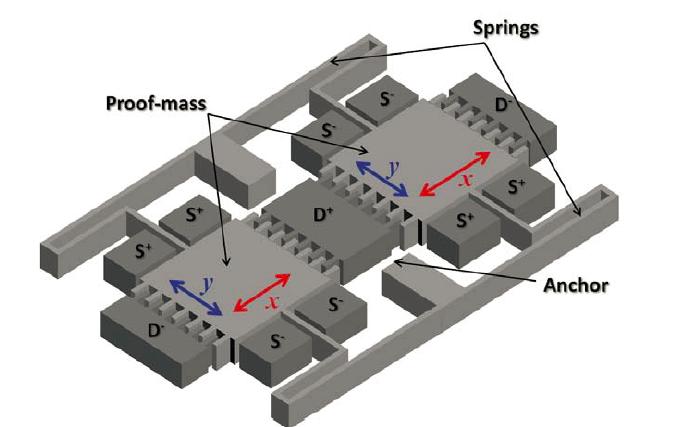
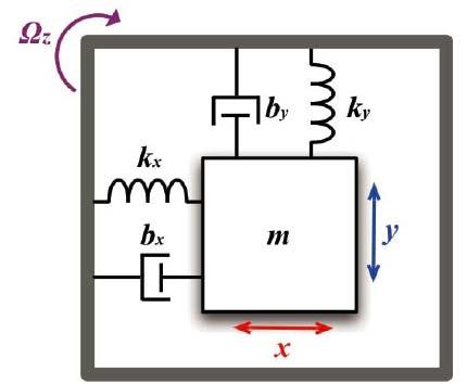
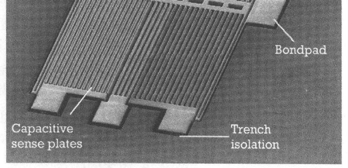
6 Polycrystalline Silicon Gyroscope

7 Effects of Residual Stress in MEMS Device Elements micromachined cantilever: e.g. for a voltage actuated mechanical switch micromachined doubly supported beam: e.g. for a voltage actuated mechanical switch
8 Effects of Residual Stress in MEMS Device Elements cantilever: minor residual stress gradients in the films can cause upward or downward curvature when the beam is released, increasing or decreasing the pull-in voltage, or making device non-functional. doubly supported beam: residual tensile stress in the films leads to an increased stiffness of the beam to be high and increase the pull-in voltage

9 Effects of Residual Stress in MEMS Device Elements cantilever: minor residual stress gradients in the films can cause upward or downward curvature when the beam is released, increasing or decreasing the pull-in voltage, or making device non-functional. doubly supported beam: residual compressive stress in the films can cause the beam to buckle, and make the device non-functional
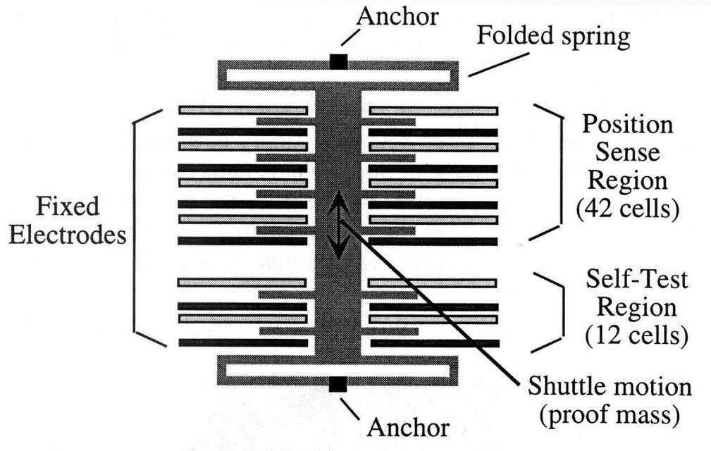
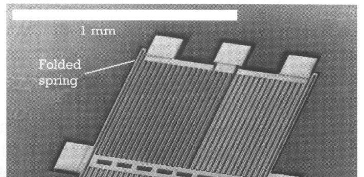
10 Polycrystalline Silicon Accelerometer (Novasensor)
11 Residual Stress: Buckling Control in the range of 10 s of MPa is required (Nunan et al, Vacuum Technology and Coating, Jan. 2001, p.27: Analog Devices)
12 Residual Stress in As-Deposited Thin Films Stress in As-Deposited CVD Polysilicon Stress In As-Deposited Sputtered Metallic Films (Hung et al, MRS Symp. Proc. V182, p201, 1990) dominated by intrinsic stress (From Ohring, after Hoffman)


13 In-situ Real-Time Intrinsic Stress Monitoring evaporative deposition UHV e-beam deposition system with load-lock, LEED, and stress sensor. Deposit on cantilever. Measure cantilever deflection. Measure capacitance change to monitor tip-displacement Sensitivity: <1ML equivalent at 100Hz
14 Stoney s Equation: Instantaneous Stress 6 = instantaneous surface stress units stress-thickness or force per width = average stress in the film = film thickness = thickness of the beam = biaxial modulus of the beam
15 Stress Evolution in Polycrystalline Films via Evaporative Deposition ~1 GPa tensile instantaneous stress e.g. Ti, W, Cr e.g. Au, Ag, Cu after R. Abermann, Vacuum 41, 1279 (1990).

16 Structure Evolution During Deposition of Polycrystalline Thin Films (C.V. Thompson, Ann. Rev. Mat. Sci. 2000)
17 Stress and Structure Co-Evolution During Film Deposition Completion of coalescence Type I tensile average stress (GPa) Type II compressive Beginning of coalescence


 etalon 25 A 40 A 55 A 2.5 nm 4.")
18 Aluminum Deposited on Oxidized Silicon stress-thickness (N/m) o C 0.2 nm/sec Al Data collected by J.A. Floro and S.J. Hearne Sandia National Laboratory J. A. Floro, S. J. Hearne, J. A. Hunter, and P. Kotula, E. Chason, S. C. Seel and C. V. Thompson, J. Appl. Phys. 89, 4886 (2001) film thickness (nm) etalon 25 A 40 A 55 A 2.5 nm 4.0 nm 5.5 nm 1000 nm Å

19 Tensile Stress Generation Due to Island Coalescence Surface Energy s Grain Boundary Energy gb 2 s gb r E 1 1 / 2 W.D. Nix and B.M. Clemens, J. Mater. Res. 14, 3467 (1999).
20 Comparison of Models for Coalescence Stress Coalescence of Ag islands with 90 0 contact angle with substrate Average stress (GPa) Freund- Chason Nix-Clemens FEM* Modified Nix-Clemens Finite Element Model: (Coalescing half-cylinders) Island radius (nm) Modified Nix-Clemens: 1 E (2 s gb) 9(1 2) r 1 2 Freund-Chason: 2(2 s gb r ) W.D. Nix and B.M. Clemens, J. Mater. Res. 14, 3467 (1999). Modified N-C: S.C. Seel Ph.D. Thesis, MIT (2002) L.B. Freund and E. Chason, J. Appl. Phys. 89, 4866 (2001). FEM: S.C. Seel, C.V. Thompson, S.J. Hearne and J.A. Floro, J. Appl. Phys 88, (2000).


21 Stress and Structure Co-Evolution During Film Deposition Completion of coalescence Type I tensile average stress (GPa) Type II compressive Beginning of coalescence
22 Data from in-situ Stress Measurements (stress-thickness) Type i: e.g. Pt 300K Type II: e.g. Au 300K Hang Yu and C.V. Thompson, Acta Materialia 67, 189 (2014)
. Chason et al: Deposition flux affects adatom population and excess chemical potential.")
23 The Origin of The Compressive Stress Type II Behavior Trapping of excess adatoms in grain boundaries during deposition W. D. Nix, and B. M. Clemens, J. Mater. Res. 14, 3467 (1999) E. Chason, B.W. Sheldon, and L. B. Freund, J. A. Floro and S. J. Hearne, PRL 88, (2002). Chason et al: Deposition flux affects adatom population and excess chemical potential. The jump from surface sites into the grain boundary sites is thermally activated.
24 Data From in-situ Stress Measurements (stress-thickness) Type i: e.g. Pt 300K Type II: e.g. Au 300K H. Yu and C.V. Thompson, Acta Materialia 67, 189 (2014)
25 Intermediate Stress Behavior effect of substrate temperature (stress-thickness) H. Yu and C.V. Thompson, Acta Materialia 67, 189 (2014)
26 stress-thickness = surface stress = force/width (N/m) Intermediate Stress Behavior effect of deposition rate Ni deposited at 473K H. Yu and C.V. Thompson, Acta Materialia 67, 189 (2014)

27 What Causes the Stress Turnaround in Intermediate Behavior tensile compressive tensile coalescence stress trapping of excess atoms? film thickening grain growth during deposition

28 Grain Growth During Film Deposition Ni Ni: T =300K T homologous = 0.17 grain growth occurs at low homologous temperatures in nanocrystalline materials H.Z. Yu, J.S. Leib, S.T. Boles, and C.V. Thompson, J. Appl. Phys. 115, (2014).
29 Grain Growth Stress Grain boundaries have excess free volume Grain growth in unconstrained films would lead to densification In films attached to substrates, without sliding, grain growth leads to a tensile stress 1 1 = biaxial modulus = the excess volume per boundary area (~0.1nm) = the initial grain size = the final grain size P. Chaudhari, IBM J. Res. Dev. 197 (1969) C. V. Thompson, and R. Carel, J. Mech. Phys. Solids 44, 657 (1996).
30 Au films 2 : Stress Evolution During Growth Interruptions A fast process leads to reversible stress evolution during grain growth 1 The fast process is related to surface phenomena (not thickness dependent) 2,3 A slow process leads to irreversible stress 2 The slow process involves a bulk phenomenon (film thickness dependent) 2 (1) A. L. Shull and F. Spaepen, J. Appl. Phys. 80(11), (1996). (2) H.Z. Yu, J.S. Leib, S.T. Boles, and C.V. Thompson, J. Appl. Phys. 115, (2014). (3) H.Z. Yu and C.V. Thompson, Appl. Phys. Letts. 104, (2014).
.")
31 Grain Growth After Deposition 0.5hrs 10hrs 26hrs 45nm Au 300K H.Z. Yu, J.S. Leib, S.T. Boles, and C.V. Thompson, J. Appl. Phys. 115, (2014).
32 Influence of Grain Growth on Stress During Deposition on the Instantaneous Stress During a very small period of time, the bulk stress increases 1 1 Δ The measured force per unit width increases The instantaneous stress is: Δ Δ Δ Δ empirically: so: H. Yu and C.V. Thompson, Acta Materialia 67, 189 (2014)
33 Grain Growth Stress During Deposition of Nanocrystalline Films The grain size at coalescence ~ 1nm Grain growth during film thickening leads yielding Modified expression for instantaneous stress accounting for yielding: Δ 1 1
34 Three Mechanisms for Stress Evolution coalescence stress: tensile 1 grain growth during deposition: tensile 1 (very approximately) post-coalescence adatom trapping: compressive Chason Model 1

35 Modification of Chason Model Assume that only adatoms within a diffusion distance can be trapped in the grain boundaries is limited by the steady state ledge spacing, affected by ledge nucleation rate on terraces / D SD = surface diffusivity R = deposition rate = lattice parameter d < 2 collection area is the total area and is fixed 1 d > 2 collection area scales with d independent of d H. Yu and C.V. Thompson, Acta Materialia 67, 189 (2014)
36 Post-Coalescence Stress Transition with Increasing Thickness/Grain Size Δ 1 1 d > 2 tensile d < 2 compressive H. Yu and C.V. Thompson, Acta Materialia 67, 189 (2014)
37 Compressive Component of the Intrinsic Stress ~ dashed line d = 2 Stress measurements with stress due to grain growth removed (based on characterization of post deposition grain growth) H. Yu and C.V. Thompson, Acta Materialia 67, 189 (2014)

 textured Ni surfaces is 0.21eV.")
38 Activation Energy for Adatom diffusion (200) (111) / / 6 The activation energy for adatom diffusion on (111) textured Ni surfaces is 0.21eV. H. Yu and C.V. Thompson, Acta Materialia 67, 189 (2014)
39 Stress Evolution Model both T and R dependencies are captured H. Yu and C.V. Thompson, Acta Materialia 67, 189 (2014)
40 Explanations for Type I and Type II Behavior Type I: Epitaxial inheritance of tensile coalescence stress (no grain growth or trapping) Type II: Turnaround at very large film thickness H. Yu and C.V. Thompson, Acta Materialia 67, 189 (2014)
41 Generalization for fcc Metals H. Yu and C.V. Thompson, Acta Materialia 67, 189 (2014)
42 Stress Evolution as a Function of Incidence Angle H.Z. Yu and C.V. Thompson, Acta Materialia 77, 284 (2014).


43 Stress Evolution as a Function of Incidence Angle 115nm Au = 0 o = 60 o roughness H.Z. Yu and C.V. Thompson, Acta Materialia 77, 284 (2014).
.")
44 Stress Evolution as a Function of Incidence Angle increased shadowing of the gb region reduced compressive component H.Z. Yu and C.V. Thompson, Acta Materialia 77, 284 (2014).
45 Stress Evolution as a Function of Incidence Angle grain size still scales with film thickness for all s H.Z. Yu and C.V. Thompson, Acta Materialia 77, 284 (2014).
46 Stress Evolution as a Function of Incidence Angle As tilt angle goes up: Peak tensile thickness goes up (larger coalescence thickness) Less compressive stress H.Z. Yu and C.V. Thompson, Acta Materialia 77, 284 (2014).
47 Stress Evolution as a Function of Incidence Angle H.Z. Yu and C.V. Thompson, Acta Materialia 77, 284 (2014).
48 Summary and Conclusions The intrinsic stress in polycrystalline vapor deposited thin films strongly depends on: the deposition technique the film thickness the substrate temperature the deposition rate the deposition angle impurities from the background pressure (not discussed here) In evaporative deposition, stress evolution is affected by three mechanisms coalescence strains (tensile) adatom trapping (compressive) grain growth (tensile) Plasticity plays a critical role in defining the intrinsic stress: due to deformation during coalescence and grain growth.
Effects of Film Thickness on the Yielding Behavior of Polycrystalline Gold Films
 Effects of Film Thickness on the Yielding Behavior of Polycrystalline Gold Films H.D. Espinosa and B.C. Prorok Department of Mechanical Engineering, Northwestern University Evanston, IL 628-3111, USA ABSTRACT
X-ray optical thin film deposition and analysis capability at NASA MSFC. D. Broadway. 11/8/2017 D. Broadway NASA MSFC 1
 X-ray optical thin film deposition and analysis capability at ASA MSFC D. Broadway /8/7 D. Broadway ASA MSFC Talk Outline Optical thin film coating capability at MSFC Deposition system X-ray reflectometer
Understanding residual stress in polycrystalline thin films through real-time. measurements and physical models. Eric Chason and Pradeep R.
 Understanding residual stress in polycrystalline thin films through real-time measurements and physical models Eric Chason and Pradeep R. Guduru School of Engineering Brown University, Providence, RI Abstract
Micro-Electro-Mechanical Systems (MEMS) Fabrication. Special Process Modules for MEMS. Principle of Sensing and Actuation
 Fabrication. Special Process Modules for MEMS. Principle of Sensing and Actuation") Micro-Electro-Mechanical Systems (MEMS) Fabrication Fabrication Considerations Stress-Strain, Thin-film Stress, Stiction Special Process Modules for MEMS Bonding, Cavity Sealing, Deep RIE, Spatial forming
Micro-Electro-Mechanical Systems (MEMS) Fabrication Fabrication Considerations Stress-Strain, Thin-film Stress, Stiction Special Process Modules for MEMS Bonding, Cavity Sealing, Deep RIE, Spatial forming
INTERFACES AND STRESSES IN THIN FILMS p
 Acta mater. 48 (2000) 31±42 www.elsevier.com/locate/actamat INTERFACES AND STRESSES IN THIN FILMS p F. SPAEPEN Division of Engineering and Applied Sciences, Harvard University, Cambridge, MA 02138, USA
Micro-Electro-Mechanical Systems (MEMS) Fabrication. Special Process Modules for MEMS. Principle of Sensing and Actuation
 Fabrication. Special Process Modules for MEMS. Principle of Sensing and Actuation") Micro-Electro-Mechanical Systems (MEMS) Fabrication Fabrication Considerations Stress-Strain, Thin-film Stress, Stiction Special Process Modules for MEMS Bonding, Cavity Sealing, Deep RIE, Spatial forming
Micro-Electro-Mechanical Systems (MEMS) Fabrication Fabrication Considerations Stress-Strain, Thin-film Stress, Stiction Special Process Modules for MEMS Bonding, Cavity Sealing, Deep RIE, Spatial forming
Poly-SiGe MEMS actuators for adaptive optics
 Poly-SiGe MEMS actuators for adaptive optics Blake C.-Y. Lin a,b, Tsu-Jae King a, and Richard S. Muller a,b a Department of Electrical Engineering and Computer Sciences, b Berkeley Sensor and Actuator
Buckling behavior of metal film/substrate structure under pure bending
 Buckling behavior of metal film/substrate structure under pure bending Ying Li, Xi-Shu Wang a Department of Engineering Mechanics, Tsinghua University, Beijing, 100084, P.R. China Xiang-Kang Meng National
Micro-Electro-Mechanical Systems (MEMS) Fabrication. Special Process Modules for MEMS. Principle of Sensing and Actuation
 Fabrication. Special Process Modules for MEMS. Principle of Sensing and Actuation") Micro-Electro-Mechanical Systems (MEMS) Fabrication Fabrication Considerations Stress-Strain, Thin-film Stress, Stiction Special Process Modules for MEMS Bonding, Cavity Sealing, Deep RIE, Spatial forming
Micro-Electro-Mechanical Systems (MEMS) Fabrication Fabrication Considerations Stress-Strain, Thin-film Stress, Stiction Special Process Modules for MEMS Bonding, Cavity Sealing, Deep RIE, Spatial forming
Interconnects. Outline. Interconnect scaling issues Aluminum technology Copper technology. Properties of Interconnect Materials
 Interconnects Outline Interconnect scaling issues Aluminum technology Copper technology 1 Properties of Interconnect Materials Metals Silicides Barriers Material Thin film Melting resistivity point ( C)
Anomaly of Film Porosity Dependence on Deposition Rate
 Anomaly of Film Porosity Dependence on Deposition Rate Stephen P. Stagon and Hanchen Huang* Department of Mechanical Engineering, University of Connecticut, Storrs, CT 06269 J. Kevin Baldwin and Amit Misra
Synthesis of nanoscale CN x /TiAlN multilayered coatings by ion-beam-assisted deposition
 Synthesis of nanoscale / multilayered coatings by ion-beam-assisted deposition M. Cao, D. J. Li, a and X. Y. Deng College of Physics and Electronic Information Science, Tianjin Normal University, Tianjin
Epitaxy is the deposition of layers, which are monocrystalline in large regions
 Repetition: Epitaxy Epitaxy is the deposition of layers, which are monocrystalline in large regions Homoepitaxy: Substrate material = film material Heteroepitaxy: Substrate material film material Repetition:
Lecture 12. Physical Vapor Deposition: Evaporation and Sputtering Reading: Chapter 12. ECE Dr. Alan Doolittle
 Lecture 12 Physical Vapor Deposition: Evaporation and Sputtering Reading: Chapter 12 Evaporation and Sputtering (Metalization) Evaporation For all devices, there is a need to go from semiconductor to metal.
Deposition and characterization of sputtered ZnO films
 Superlattices and Microstructures 42 (2007) 89 93 www.elsevier.com/locate/superlattices Deposition and characterization of sputtered ZnO films W.L. Dang, Y.Q. Fu, J.K. Luo, A.J. Flewitt, W.I. Milne Electrical
GaN Stress Evolution During Metal-Organic Chemical Vapor Deposition
 GaN Stress Evolution During Metal-Organic Chemical Vapor Deposition S. Hearnea, E. Chason, J. Han, J. A. Floro, J. Figiel, J. Hunter Sandia National Laboratories, Albuquerque, New Mexico 87185 H. Amano
In-situ Study of Solid Electrolyte Interphase on Silicon Electrodes using PeakForce Tapping Mode AFM in Glove-box
 General Motors R&D BROWN UNIVERSITY In-situ Study of Solid Electrolyte Interphase on Silicon Electrodes using PeakForce Tapping Mode AFM in Glove-box A. Tokranov 1, X. Xiao 2, C. Li 3, S. Minne 3 and B.
Deformation of Blanketed and Patterned Bilayer Thin-Film Microstructures During Post-Release and Cyclic Thermal Loading
 788 JOURNAL OF MICROELECTROMECHANICAL SYSTEMS, VOL. 12, NO. 6, DECEMBER 2003 Deformation of Blanketed and Patterned Bilayer Thin-Film Microstructures During Post-Release and Cyclic Thermal Loading Yanhang
Analysis and modeling of residual stress in diamond thin film deposited by the hot-filament chemical vapor deposition process
 Analysis and modeling of residual stress in diamond thin film deposited by the hot-filament chemical vapor deposition process Seung I. Cha and Soon H. Hong Department of Materials Science and Engineering,
Structural changes of polycrystalline silicon layers during high temperature annealing
 Structural changes of polycrystalline silicon layers during high temperature annealing D. Lysáček, L. Válek ON SEMICONDUCTOR CZECH REPUBLIC, Rožnov p. R., david.lysacek@onsemi.com Abstract The structure
Probing Interfacial Contact via MEMS-based Microinstrumentation
 Probing Interfacial Contact via MEMS-based Microinstrumentation Roya Maboudian Department of Chemical & Biomolecular Engineering Berkeley Sensor and Actuator Center (BSAC) Center of Integrated Nanomechanical
Previous Lecture. Vacuum & Plasma systems for. Dry etching
 Previous Lecture Vacuum & Plasma systems for Dry etching Lecture 9: Evaporation & sputtering Objectives From this evaporation lecture you will learn: Evaporator system layout & parts Vapor pressure Crucible
Stress and Microstructure in Electrodeposited Copper Nanofilms by Substrate Curvature and In-situ Electrochemical AFM Measurements
 10.1149/1.2909720 The Electrochemical Society Stress and Microstructure in Electrodeposited Copper Nanofilms by Substrate Curvature and In-situ Electrochemical AFM Measurements S. Ahmed, T. T. Ahmed, M.
Direct Measurement of the Nanoscale Mechanical Properties of NiTi Shape Memory Alloy
 Mat. Res. Soc. Symp. Proc. Vol. 791 2004 Materials Research Society Q7.11.1 Direct Measurement of the Nanoscale Mechanical Properties of NiTi Shape Memory Alloy Gordon A. Shaw 1, Wendy C. Crone 2 1 Department
Latching Shape Memory Alloy Microactuator
 Latching Shape Memory Alloy Microactuator ENMA490, Fall 00 S. Cabrera, N. Harrison, D. Lunking, R. Tang, C. Ziegler, T. Valentine Outline Background Problem Project Development Design Evaluation Applications
Tensile Testing of Polycrystalline Silicon Thin Films Using Electrostatic
 Paper Tensile Testing of Polycrystalline Silicon Thin Films Using Electrostatic Force Grip Member Toshiyuki Tsuchiya (Toyota Central Labs., Inc.) Member Osamu Tabata (Ritsumeikan University) Jiro Sakata
PHYS 534 (Fall 2008) Process Integration OUTLINE. Examples of PROCESS FLOW SEQUENCES. >Surface-Micromachined Beam
 Process Integration OUTLINE. Examples of PROCESS FLOW SEQUENCES. >Surface-Micromachined Beam") PHYS 534 (Fall 2008) Process Integration Srikar Vengallatore, McGill University 1 OUTLINE Examples of PROCESS FLOW SEQUENCES >Semiconductor diode >Surface-Micromachined Beam Critical Issues in Process
PHYS 534 (Fall 2008) Process Integration Srikar Vengallatore, McGill University 1 OUTLINE Examples of PROCESS FLOW SEQUENCES >Semiconductor diode >Surface-Micromachined Beam Critical Issues in Process
Growth and Doping of SiC-Thin Films on Low-Stress, Amorphous Si 3 N 4 /Si Substrates for Robust Microelectromechanical Systems Applications
 Journal of ELECTRONIC MATERIALS, Vol. 31, No. 5, 2002 Special Issue Paper Growth and Doping of SiC-Thin Films on Low-Stress, Amorphous Si 3 N 4 /Si Substrates for Robust Microelectromechanical Systems
5. A round rod is subjected to an axial force of 10 kn. The diameter of the rod is 1 inch. The engineering stress is (a) MPa (b) 3.
 MPa (b) 3.") The Avogadro's number = 6.02 10 23 1 lb = 4.45 N 1 nm = 10 Å = 10-9 m SE104 Structural Materials Sample Midterm Exam Multiple choice problems (2.5 points each) For each problem, choose one and only one
The Avogadro's number = 6.02 10 23 1 lb = 4.45 N 1 nm = 10 Å = 10-9 m SE104 Structural Materials Sample Midterm Exam Multiple choice problems (2.5 points each) For each problem, choose one and only one
Calculation of Stress And Deflection In Double Layer Microcantilever For Biosensor Application
 Calculation of Stress And Deflection In Double Layer Microcantilever For Biosensor Application 1,2 Lia Aprilia, 1 Ratno Nuryadi, 2 Djoko Hartanto 1 Center for Material Technology, Agency for the Assessment
Nucleation and growth of nanostructures and films. Seongshik (Sean) Oh
 Oh") Nucleation and growth of nanostructures and films Seongshik (Sean) Oh Outline Introduction and Overview 1. Thermodynamics and Kinetics of thin film growth 2. Defects in films 3. Amorphous, Polycrystalline
Nucleation and growth of nanostructures and films Seongshik (Sean) Oh Outline Introduction and Overview 1. Thermodynamics and Kinetics of thin film growth 2. Defects in films 3. Amorphous, Polycrystalline
A Phase Field Model for Grain Growth and Thermal Grooving in Thin Films with Orientation Dependent Surface Energy
 Solid State Phenomena Vol. 129 (2007) pp. 89-94 online at http://www.scientific.net (2007) Trans Tech Publications, Switzerland A Phase Field Model for Grain Growth and Thermal Grooving in Thin Films with
In-situ nano-mechanical tests in the light of μlaue diffraction
 Engineering Conferences International ECI Digital Archives Nanomechanical Testing in Materials Research and Development V Proceedings Fall 10-8-2015 In-situ nano-mechanical tests in the light of μlaue
Electrochemical Oxidation, Threading Dislocations and the Reliability of GaN HEMTs
 Electrochemical Oxidation, Threading Dislocations and the Reliability of GaN HEMTs Carl V. Thompson 1,3 Dept. of Materials Science and Engineering, M.I.T. Primary collaborators: Wardhana A. Sasangka 1,
SOLID SOLUTION METAL ALLOYS
 SOLID SOLUTION METAL ALLOYS Synergy Effects vs. Segregation Phenomena D. Manova, J. Lutz, S. Mändl, H. Neumann 1 Table of Content Motivation Alloys vs. Pure Elements or Intermetallic Compounds Introduction
Laser Annealing of Amorphous Ni-Ti Shape Memory Alloy Thin Films
 Laser Annealing of Amorphous Ni-Ti Shape Memory Alloy Thin Films Xi Wang, Zhenyu Xue, Joost J. Vlassak Division of Engineering and Applied Sciences, Harvard University, Cambridge, MA, U.S.A. Yves Bellouard
The Material (in) Dependency of Impurity Affected Thin Film Growth
 Dependency of Impurity Affected Thin Film Growth") The Material (in) Dependency of Impurity Affected Thin Film Growth F. Cougnon, D. Altangerel, R. Dedoncker, D. Depla Dedicated Research on Advanced Films and Targets Ghent University Answering some questions.
The Material (in) Dependency of Impurity Affected Thin Film Growth F. Cougnon, D. Altangerel, R. Dedoncker, D. Depla Dedicated Research on Advanced Films and Targets Ghent University Answering some questions.
Chapter 2 OVERVIEW OF MEMS
 6 Chapter 2 OVERVIEW OF MEMS 2.1 MEMS and Microsystems The term MEMS is an abbreviation of microelectromechanical system. MEMS contains components ofsizes in 1 micrometer to 1 millimeter. The core element
MICRO-ELECTRO-MECHANICAL VARIABLE BLAZE GRATINGS
 MICRO-ELECTRO-MECHANICAL VARIABLE BLAZE GRATINGS D. M. Burns and V. M. Bright Air Force Institute of Technology Department of Electrical and Computer Engineering Wright-Patterson Air Force Base, OH 45433-7765
Mechanical Properti es of ZnO:Mo Transparent Conducting Oxide Thin Film Prepared by Sputtering
 CHINESE JOURNAL OF PHYSICS VOL. 51, NO. 3 June 2013 Mechanical Properti es of ZnO:Mo Transparent Conducting Oxide Thin Film Prepared by Sputtering Y. C. Lin, C. C. Chen, and W. Y. Lai Department of Mechatronics
Lattice Kinetic Monte Carlo: Building a bridge between ab-initio calculations and process simulation
 Lattice Kinetic Monte Carlo: Building a bridge between ab-initio calculations and process simulation Polycrystalline Materials E. Rubio, M. Jaraiz, L.A. Bailon, J. Barbolla, M.J. Lopez University of Valladolid,
Metallorganic Chemical Vapor Deposition of Ru Films Using Cyclopentadienyl-Propylcyclopentadienylruthenium II and Oxygen
 0013-4651/2002/149 6 /C317/7/$7.00 The Electrochemical Society, Inc. Metallorganic Chemical Vapor Deposition of Ru Films Using Cyclopentadienyl-Propylcyclopentadienylruthenium II and Oxygen Sang Yeol Kang,
Silver Diffusion Bonding and Layer Transfer of Lithium Niobate to Silicon
 Chapter 5 Silver Diffusion Bonding and Layer Transfer of Lithium Niobate to Silicon 5.1 Introduction In this chapter, we discuss a method of metallic bonding between two deposited silver layers. A diffusion
Institute of Solid State Physics. Technische Universität Graz. Deposition. Franssila: Chapters 5 & 6. Peter Hadley
 Technische Universität Graz Institute of Solid State Physics Deposition Franssila: Chapters 5 & 6 Peter Hadley Silicon wafers Total Thickness Variation: a good 8" Prime wafer would be < 15 m Site flatness
Procedia Chemistry 1 (2009) Proceedings of the Eurosensors XXIII conference
 Proceedings of the Eurosensors XXIII conference") Procedia Chemistry 1 (2009) 609 613 Procedia Chemistry www.elsevier.com/locate/procedia Proceedings of the Eurosensors XXIII conference Thermal Characterization of Polycrystalline CVD Diamond Thin Films
Procedia Chemistry 1 (2009) 609 613 Procedia Chemistry www.elsevier.com/locate/procedia Proceedings of the Eurosensors XXIII conference Thermal Characterization of Polycrystalline CVD Diamond Thin Films
Magnetic patterning: local manipulation of the intergranular. exchange coupling via grain boundary engineering
 Magnetic patterning: local manipulation of the intergranular exchange coupling via grain boundary engineering Kuo-Feng Huang, 1 Jung-Wei Liao, 1 Cheng-Yu Hsieh, 2 Liang-Wei Wang, 1 Yen-Chun Huang, 1 Wei-Chih
Moisture Effects on Copper Thin Film Adhesion
 Conference Proceedings of ASME 25 Congress International Mechanical Engineering Congress and Exposition November 5-11, 25 Orlando Florida 81532 Moisture Effects on Copper Thin Film Adhesion Patrick J.
Control of buckling in large nanomembranes using engineered support structures
 Control of buckling in large nanomembranes using engineered support structures Eiji Iwase 1, Pui-Chuen Hui 1, David Woolf 1, Alejandro W. Rodriguez 1,2, Steven G. Johnson 2, Federico Capasso 1, Marko Loncar
High-resolution electron microscopy of grain boundary structures in yttria-stabilized cubic zirconia
 Mat. Res. Soc. Symp. Proc. Vol. 654 2001 Materials Research Society High-resolution electron microscopy of grain boundary structures in yttria-stabilized cubic zirconia K. L. Merkle, L. J. Thompson, G.-R.
High Anisotropy L1 0 FePt Media for Perpendicular Magnetic Recording Applications
 DISKCON 2008 High Anisotropy L1 0 FePt Media for Perpendicular Magnetic Recording Applications Boon Chow LIM Agency for Science Technology & Research (A*STAR) DATA STORAGE INSTITUTE 5 Engineering Drive
Development of High Throughput CIGS Manufacturing Process. PI: Neelkanth Dhere Students: Sachin Kulkarni, Ph.D.; Ph.D.; Ashwani Kaul, Ph.D.
 UNIVERSITY OF CENTRAL FLORIDA Development of High Throughput CIGS Manufacturing Process PI: Neelkanth Dhere Students: Sachin Kulkarni, Ph.D.; Ph.D.; Ashwani Kaul, Ph.D. Description: A reduction in the
Enhancement of Copper Wetting via Surfactant-Based Post-Treatment of Ultra-Thin Atomic Layer Deposited Tantalum Nitride Liners
 Mat. Res. Soc. Symp. Proc. Vol. 766 2003 Materials Research Society E10.3.1 Enhancement of Copper Wetting via Surfactant-Based Post-Treatment of Ultra-Thin Atomic Layer Deposited Tantalum Nitride Liners
More Thin Film X-ray Scattering and X-ray Reflectivity
 Stanford Synchrotron Radiation Laboratory More Thin Film X-ray Scattering and X-ray Reflectivity Mike Toney, SSRL 1. Introduction (real space reciprocal space) 2. Polycrystalline film (no texture) RuPt
Development of New Generation Of Coatings with Strength-Ductility Relationship, Wear, Corrosion and Hydrogen Embrittlement Resistance Beyond the
 Development of New Generation Of Coatings with Strength-Ductility Relationship, Wear, Corrosion and Hydrogen Embrittlement Resistance Beyond the Current Materials Accomplishments till date As the structural
Influence of Underlayer on Crystallography and Roughness of Aluminum Nitride Thin Film Reactively Sputtered by Ion-Beam Kaufman Source
 Influence of Underlayer on Crystallography and Roughness of Aluminum Nitride Thin Film Reactively Sputtered by Ion-Beam Kaufman Source GABLECH Imrich 1,*, SVATOŠ Vojtěch 1,, PRÁŠEK Jan 1,, HUBÁLEK Jaromír
Modeling of stresses and deformation in thin film and interconnect line structures
 Modeling of stresses and deformation in thin film and interconnect line structures Adam Wikström Doctoral Thesis Department of Solid Mechanics Royal Institute of Technology Stockholm 2001 Preface The research
THE INFLUENCE OF NITROGEN CONTENT ON THE MECHANICAL PROPERTIES OF TiN x THIN FILMS PREPARED BY REACTIVE MAGNETRON SPUTTERING
 Bulletin of the Transilvania University of Braşov Series I: Engineering Sciences Vol. 5 (54) No. 2-2012 THE INFLUENCE OF NITROGEN CONTENT ON THE MECHANICAL PROPERTIES OF TiN x THIN FILMS PREPARED BY REACTIVE
Microstructures using RF sputtered PSG film as a sacrificial layer in surface micromachining
 Sādhanā Vol. 34, Part 4, August 2009, pp. 557 562. Printed in India Microstructures using RF sputtered PSG film as a sacrificial layer in surface micromachining VIVEKANAND BHATT 1,, SUDHIR CHANDRA 1 and
PHYSICAL PROPERTIES OF AU AND AL THIN FILMS MEASURED BY RESISTIVE HEATING
 Surface Review and Letters, Vol. 12, No. 1 (2005) 101 106 c World Scientific Publishing Company PHYSICAL PROPERTIES OF AU AND AL THIN FILMS MEASURED BY RESISTIVE HEATING F. AVILÉS,O.CEHandA.I.OLIVA Centro
Mechanical Limitations of Materials for Steel Foil Based Flexible Electronics
 Mater. Res. Soc. Symp. Proc. Vol. 30 2008 Materials Research Society 30-G03-14 Mechanical Limitations of Materials for Steel Foil Based Flexible Electronics Po-Chin Kuo 1, Vasilios G. Chouvardas 2, Jeff
Torsional properties of bamboo-like structured Cu nanowires. Haifei Zhan and Yuantong Gu *
 Torsional properties of bamboo-like structured Cu nanowires Haifei Zhan and Yuantong Gu * School of Chemistry, Physics and Mechanical Engineering, Queensland University of Technology, Brisbane, QLD, 4001,
Ageing Resistance (12 years) of Hard and Oxidation Resistant SiBCN Coatings
 of Hard and Oxidation Resistant SiBCN Coatings") Ageing Resistance (12 years) of Hard and Oxidation Resistant SiBCN Coatings Jiri Houska Department of Physics and NTIS - European Centre of Excellence, University of West Bohemia, Czech Republic Acknowledgment
Ageing Resistance (12 years) of Hard and Oxidation Resistant SiBCN Coatings Jiri Houska Department of Physics and NTIS - European Centre of Excellence, University of West Bohemia, Czech Republic Acknowledgment
Fabrication and Characterization of Fe-Pd Ferromagnetic Shape-Memory Thin Films
 Mat. Res. Soc. Symp. Proc. Vol. 785 24 Materials Research Society D7.4.1 Fabrication and Characterization of Fe-Pd Ferromagnetic Shape-Memory Thin Films Yuki Sugimura, Tzahi Cohen-Karni, Patrick McCluskey
Morphology of Thin Aluminum Film Grown by DC Magnetron Sputtering onto SiO 2 on Si(100) Substrate
 Substrate") Morphology of Thin Aluminum Film Grown by DC Magnetron Sputtering onto SiO 2 on Si(1) Substrate Fan Wu Microelectronics Center, Medtronic Inc., Tempe, AZ 85261 James E. Morris Department of Electrical
Morphology of Thin Aluminum Film Grown by DC Magnetron Sputtering onto SiO 2 on Si(1) Substrate Fan Wu Microelectronics Center, Medtronic Inc., Tempe, AZ 85261 James E. Morris Department of Electrical
Properties of TiN thin films grown on SiO 2 by reactive HiPIMS
 Properties of TiN thin films grown on SiO 2 by reactive HiPIMS Friðrik Magnus 1, Árni S. Ingason 1, Ólafur B. Sveinsson 1, S. Shayestehaminzadeh 1, Sveinn Ólafsson 1 and Jón Tómas Guðmundsson 1,2 1 Science
Pulsed laser deposition of NdNiO 3 thin films
 Solid State Communications 136 (2005) 369 374 www.elsevier.com/locate/ssc Pulsed laser deposition of NdNiO 3 thin films Davinder Kaur a, *, J. Jesudasan b, P. Raychaudhuri b a Department of Physics, Indian
Processing of PbTiO3 thin films. III. Effects of ion bombardment
 Processing of PbTiO3 thin films. III. Effects of ion bombardment Chen C. Li and Seshu B. Desu Citation: Journal of Vacuum Science & Technology A 14, 13 (1996); doi: 10.1116/1.579910 View online: http://dx.doi.org/10.1116/1.579910
FABRICATION PROCESSES FOR MAGNETIC MICROACTUATORS WITH POLYSILICON FLEXURES. Jack W. Judy and Richard S. Muller
 FABRICATION PROCESSES FOR MAGNETIC MICROACTUATORS WITH POLYSILICON FLEXURES Jack W. Judy and Richard S. Muller Berkeley Sensor & Actuator Center (BSAC) Department of EECS, University of California, Berkeley,
2.0 Kinetic Phenomena in Thin Film Electronic Materials
 2.0 Kinetic Phenomena in Thin Film Electronic Materials Academic and Research Staff Prof. C.V. Thompson, Prof. C.G. Fonstad, Prof. H.I. Smith, Dr. R.C. Cammarata, Dr. J. Melngailis Visiting Scientist H.
This paper is part of the following report: UNCLASSIFIED
 UNCLASSIFIED Defense Technical Information Center Compilation Part Notice ADP012199 TITLE: Grain-Size-Dependent Thermal Transport Properties in Nanocrystalline Yttria-Stabilized Zirconia DISTRIBUTION:
Passive TCF Compensation in High Q Silicon Micromechanical Resonators
 Passive TCF Compensation in High Q Silicon Micromechanical Resonators A.K. Samarao, G. Casinovi and F. Ayazi IEEE International Conference on Micro Electro Mechanical Systems pp. 116 119, January 2010
The Effect of a Passivation Layer on the Anelastic Response of Gold Thin Films
 Lehigh University Lehigh Preserve Theses and Dissertations 2015 The Effect of a Passivation Layer on the Anelastic Response of Gold Thin Films Patrick Holmes Lehigh University Follow this and additional
Implications of Stress Migration and Voiding in Cu Damascene Interconnections
 Implications of Stress Migration and Voiding in Cu Damascene Interconnections E. T. Ogawa and J. W. McPherson Texas Instruments, Inc. Dallas, TX USA 22 Topical Research Conference (TRC) on Reliability,
Capillary-driven topography and microstructure evolution in metals: matching experiment with theory
 Capillary-driven topography and microstructure evolution in metals: matching experiment with theory E. Rabkin, L. Klinger, D. Amram, O. Malyi Dept. of Materials Science and Engineering, TECHNION, Haifa,
MANUFACTURING OF AN OPTICAL QUALITY MIRROR SYSTEM FOR ADAPTIVE OPTICS
 Invited Paper MNUFCTURING OF N OPTICL QULITY MIRROR SYSTEM FOR DPTIVE OPTICS Julie. Perreaulta, Paul. Bierden', Mark N. Horensteina, and Thomas G. Bifanoc aelectrical and Computer Engineering, Boston University,
 This article was originally published in a journal published by Elsevier, and the attached copy is provided by Elsevier for the author s benefit and for the benefit of the author s institution, for non-commercial
Research Article Synthesis and Characterization of LPCVD Polysilicon and Silicon Nitride Thin Films for MEMS Applications
 Materials, Article ID 954618, 8 pages http://dx.doi.org/1.1155/214/954618 Research Article Synthesis and Characterization of LPCVD Polysilicon and Silicon Nitride Thin Films for MEMS Applications N. Sharma,
Residual Stress in CVD-grown 3C-SiC Films on Si Substrates
 Mater. Res. Soc. Symp. Proc. Vol. 1069 2008 Materials Research Society 1069-D03-05 Residual Stress in CVD-grown 3C-SiC Films on Si Substrates Alex A. Volinsky 1, Grygoriy Kravchenko 1, Patrick Waters 1,
Accumulation (%) Amount (%) Particle Size 0.1
 Amount (%) Particle Size 0.1") 100 10 Amount (%) 5 50 Accumulation (%) 0 0.1 1 Particle Size (µm) 10 0 Supplementary Figure 1. The particle size distribution of W-15 at% Cr after 20 hours milling. Supplementary Figure 2. a,b, X-ray
100 10 Amount (%) 5 50 Accumulation (%) 0 0.1 1 Particle Size (µm) 10 0 Supplementary Figure 1. The particle size distribution of W-15 at% Cr after 20 hours milling. Supplementary Figure 2. a,b, X-ray
Effect of Sheet Thickness and Type of Alloys on the Springback Phenomenon for Cylindrical Die
 AMERICAN JOURNAL OF SCIENTIFIC AND INDUSTRIAL RESEARCH 01, Science Huβ, http://www.scihub.org/ajsir ISSN: 153-69X, doi:10.551/ajsir.01.3.6.80.86 Effect of Sheet Thickness and Type of Alloys on the Springback
Change in stoichiometry
 Measurement of Gas Sensor Performance Gas sensing materials: 1. Sputtered ZnO film (150 nm (Massachusetts Institute of Technology) 2. Sputtered SnO 2 film (60 nm) (Fraunhofer Institute of Physical Measurement
EE 5344 Introduction to MEMS. CHAPTER 3 Conventional Si Processing
 3. Conventional licon Processing Micromachining, Microfabrication. EE 5344 Introduction to MEMS CHAPTER 3 Conventional Processing Why silicon? Abundant, cheap, easy to process. licon planar Integrated
Nano-indentation of Nanocrystalline Tungsten A Molecular Dynamic Simulation
 Nano-indentation of Nanocrystalline Tungsten A Molecular Dynamic Simulation A.Tahiri*, M. Idiri, S. El joumani, B.Boubeker Laboratoire d'ingénierie et Matériaux (LIMAT), Faculté des Sciences Ben M Sik
Chapter 2. Density 2.65 g/cm 3 Melting point Young s modulus Tensile strength Thermal conductivity Dielectric constant 3.
 Chapter 2 Thin Film Materials Thin films of Silicon dioxide, Silicon nitride and Polysilicon have been utilized in the fabrication of absolute micro pressure sensor. These materials are studied and discussed
Repetition: Adhesion Mechanisms
 Repetition: Adhesion Mechanisms a) Mechanical interlocking b) Monolayer/monolayer c) Chemical bonding d) Diffusion e) Psedo diffusion due to augmented energy input (hyperthermal particles) Repetition:
Supplementary Figures
 Supplementary Figures Supplementary Figure 1. (a) Transmittance spectra of the TCM at different strains as tested before the fatigue test; (b) correlation between cyclic stress and cycles curve for the
Thomas M. Adams Richard A. Layton. Introductory MEMS. Fabrication and Applications. Springer
 Thomas M. Adams Richard A. Layton Introductory MEMS Fabrication and Applications Springer Contents Preface xiü Part I Fabrication Chapter 1: Introduction 3 1.1 What are MEMS? 3 1.2 Why MEMS? 4 1.2.1. Low
Proceedings Post Fabrication Processing of Foundry MEMS Structures Exhibiting Large, Out-of-Plane Deflections
 Proceedings Post Fabrication Processing of Foundry MEMS Structures Exhibiting Large, Out-of-Plane Deflections LaVern Starman 1, *, John Walton 1, Harris Hall 1 and Robert Lake 2 1 Sensors Directorate,
Next Generation High-Efficiency Low-cost Thin Film Photovoltaics
 Next Generation High-Efficiency Low-cost Thin Film Photovoltaics Investigators Bruce Clemens, Professor, Materials Science and Engineering, Stanford University, Alberto Salleo, Assistant Professor, Materials
Physics and Material Science of Semiconductor Nanostructures
 Physics and Material Science of Semiconductor Nanostructures PHYS 570P Prof. Oana Malis Email: omalis@purdue.edu Today Bulk semiconductor growth Single crystal techniques Nanostructure fabrication Epitaxial
Improving the Performance of Ceramic Barrier Layers used in Packaging Materials
 Improving the Performance of Ceramic Barrier Layers used in Packaging Materials Roland Trassl Senior Manager Advanced Development Applied Materials WEB Coating GmbH AIMCAL Tampa, Florida, USA 18 th October,
High Power Impulse Magnetron Sputtering: a Tool for Synthesizing New Functional Thin Films and Coatings
 High Power Impulse Magnetron Sputtering: a Tool for Synthesizing New Functional Thin Films and Coatings Dr. Kostas Sarakinos (Linköping University, Švédsko ) The project is co-financed by the European
Modeling of Local Oxidation Processes
 Introduction Isolation Processes in the VLSI Technology Main Aspects of LOCOS simulation Athena Oxidation Models Several Examples of LOCOS structures Calibration of LOCOS effects using VWF Field Oxide
Large-Grain Polysilicon Films with Low Intragranular Defect Density by Low- Temperature Solid-Phase Crystallization
 Mat. Res. Soc. Symp. Proc. Vol. 715 2002 Materials Research Society Large-Grain Polysilicon Films with Low Intragranular Defect Density by Low- Temperature Solid-Phase Crystallization Xiang-Zheng Bo, Nan
Time-resolved diffraction profiles and structural dynamics of Ni film under short laser pulse irradiation
 IOP Publishing Journal of Physics: Conference Series 59 (2007) 11 15 doi:10.1088/1742-6596/59/1/003 Eighth International Conference on Laser Ablation Time-resolved diffraction profiles and structural dynamics
Today s Class. Materials for MEMS
 Lecture 2: VLSI-based Fabrication for MEMS: Fundamentals Prasanna S. Gandhi Assistant Professor, Department of Mechanical Engineering, Indian Institute of Technology, Bombay, Recap: Last Class What is
Observation of Al-lines in LSI devices by ultra-high voltage electron microscope
 Microsc. Microanal. Microstruct. 4 (1993) 239 APRIUJUNE 1993, PAGE 239 Classification Physics Abstracts 07.80-73.90 Observation of Al-lines in LSI devices by ultra-high voltage electron microscope Akio
EE C245 ME C218 Introduction to MEMS Design Fall 2011
 Lecture Outline EE C245 ME C218 Introduction to MEMS Design Fall 2011 Prof. Clark T.-C. Nguyen Dept. of Electrical Engineering & Computer Sciences University of California at Berkeley Berkeley, CA 94720
Dislocation and Deformation Mechanisms in Thin Metal Films and Multilayers I
 Dislocation and Deformation Mechanisms in Thin Metal Films and Multilayers I Mat. Res. Soc. Symp. Proc. Vol. 673 2001 Materials Research Society Constrained Diffusional Creep in Thin Copper Films D. Weiss,
Fabrication Technology, Part II
 EEL5225: Principles of MEMS Transducers (Fall 2003) Fabrication Technology, Part II Agenda: Process Examples TI Micromirror fabrication process SCREAM CMOS-MEMS processes Wafer Bonding LIGA Reading: Senturia,