At wavelength characterization of EUV and soft X-ray gratings
|
|
|
- David Reynard Sharp
- 6 years ago
- Views:
Transcription
1 At wavelength characterization of EUV and soft X-ray gratings F. Scholze, A, Haase, C. Laubis, V. Soltwisch, J. Wernecke, M. Krumrey Physikalisch-Technische Bundesanstalt, Abbestraße 2-12, Berlin, Germany M. Burkhardt, A. Gatto Carl Zeiss Jena GmbH, Carl-Zeiss-Promenade 10, Jena, Germany
2 Outline PTB s EUV radiometry beamline optical characterization of a blazed grating and performance in beamline Determination of profile parameters with GISAXS Scatter from bare and coated substrate Scatter from resist pattern Conclusions 2

3 PTB laboratories in Adlershof BESSY II 3

4 PTB laboratory at BESSY II EUV 1 plane grating monochromator SX700 3c deflected undispersed bending magnet 30 nm to 0.7 nm radiation, EUV irradiation test station 2a four-crystal monochromator 4a undispersed undulator radiation 0.7 nm to 0.1 nm Compton backscattering 2b X-ray pencil beam facility (XPBF), 4b plane grating monochromator (PGM) astrophysics optics characterization at undulator, 30 nm to 0.65 nm 3a undispersed bending magnet radiation 4c deflected undispersed undulator radiation 3b normal incidence monochromator EUVL metrology test station (source calibration) 4
5 Soft X-ray radiometry beamline at BESSY II Reflectometer halo-aperture Wavelength At 13 nm Radiant Power 0.5 µw Higher diffraction orders 0.06 % Diffuse scattered light 0.2 % 0.65 nm to 25 nm sample not in focus spot at sample > 0.5 mm low divergence (< 1 mrad vert., < 2 mrad hor.) beam halo suppressed by aperture 5

6 PTB s EUV Reflectometer 5 sr collector, 670 mm outer diameter Axis Range Q -30 to 95 Tilt -10 to 10 F 0 to 360 X -90 mm to 90 mm Y -10 mm to 300 mm Z -15 mm to 140 mm Det. X 0 mm to 120 mm Det. R 150 mm to 550 mm Det. Y 0 to 180 2q -5 to 190 Accuracy: 10 µm or 0.01 at MLS from August
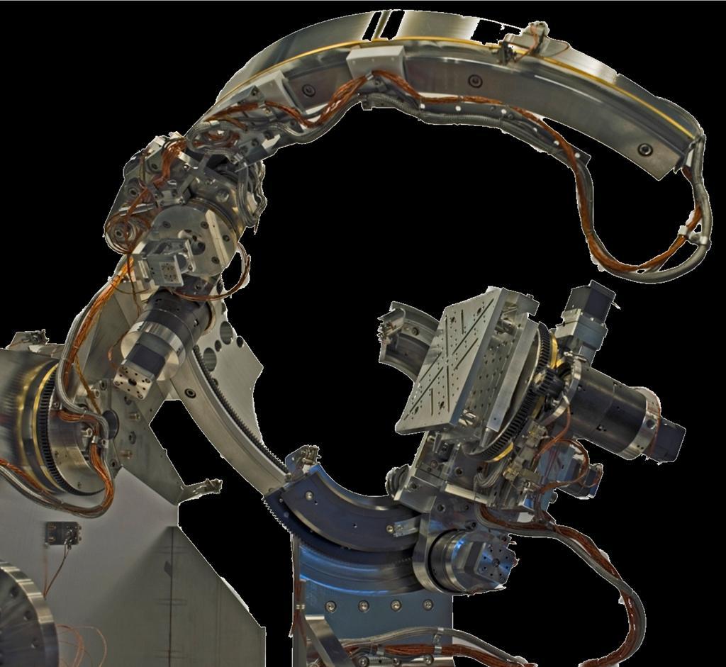

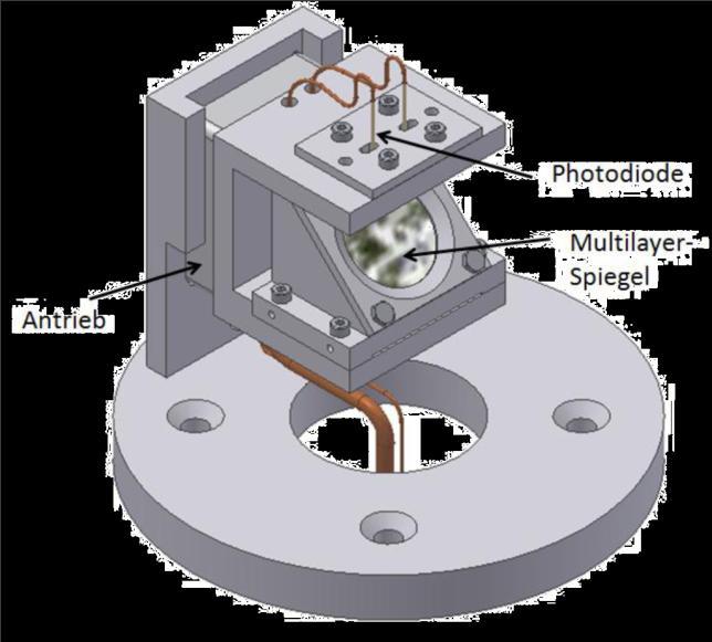

7 EUV-Ellipso-Scatterometer Linear polarization analyzer sample and detector stages of the Ellipsometer 8th-Workshop-Ellipsometry, Dresden, March

8 Measurement Scheme CCD Geometry for diffuse scatter measurements with CCD sensor EUV reflectometer at SX700 until 2013 CCD mounted at 162 included angle EUV Ellipso-scatterometer from 2013 CCD mounted at 156 included angle 8th-Workshop-Ellipsometry, Dresden, March

9 Ruled, blazed grating Grating for EUV beamline at MLS, size 150 x 70 mm² 9
10 Blazed grating, diffraction efficiency diffraction efficiency for operation in PGM-mode with c ff = l/mm, blaze 4 => rather close to suspected values diffraction efficiency for operation in PGM-mode with c ff variable high contributions of higher diffraction orders for long wavelegths 10


11 GISAXS: Schematic q k f k i q q q x y z k k k sinq cos cosq cos f i f sin sin f f f cos i Ewald sphere for gratings k 0 2 k i k f top view PM
 Determination of Ru coating thickness: 46.3(7) nm Scholze, Kato, Wernecke, Krumrey, Proc.")
12 Ruled, blazed grating, GISAXS Determination of blaze angle: 4.5(1) GISAXS at blazed grating 1200 l/mm E ph = 10 kev (log. intensity) Determination of Ru coating thickness: 46.3(7) nm Scholze, Kato, Wernecke, Krumrey, Proc. SPIE 8166, 81661P (2011) 12


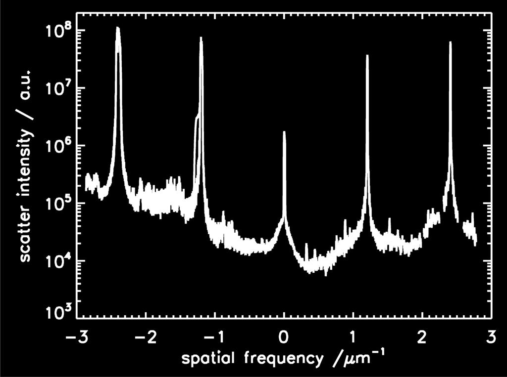
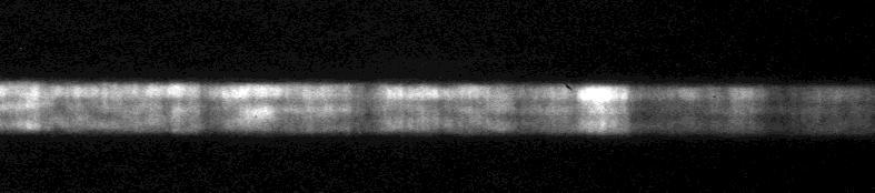
13 Ruled, blazed grating, EUV scattering = 10 nm 2Q =


14 Ruled, blazed grating, EUV scattering fine structure of diffuse scatter 14


15 Grating performance in beamline 14.5 nm Measurement of spectral distribution with flat field spectrograph 25 nm 15

16 Holographic blazed grating Diffraction efficiency of holographic blazed gratings with different blaze angles (PGM-operation, c ff =2.5) => confirmation of optimal blaze angle 4 for this application samples mounted on holder 16
17 Holographic blazed grating * 1/5 => 20x improvement w.r.t. previous grating Diffuse scatter for holographic blazed grating => Si-L edge from beamline filter visible 17


 and etch depth H")
18 Laminar Grating U. Zeitner et al., Proc SPIE 8450, 84502Z, 2012 diffraction efficiency of binary gratings with different CD (solid line 290 nm, long dashes 250 nm, dots 208 nm) and etch depth H benchmark: blazed grating 18
19 Laminar Grating: Influence of coating Diffuse scatter from a liminar grating etched into quartz extremely low diffuse scatter 10-7 with respect to 1 st. order x 0.01 => issue: sort out scatter from beamline Diffuse scatter for substrate(blue), coated (red) and no filter in beamline (green) 19


 and no filter in")
20 Laminar grating substrate bare substrate Ru coated Ru-coated substrate Observation of superstructure from e-beam writing on bare substrate and on coated grating Diffuse scatter for substrate(blue), coated (red) and no filter in beamline (green) 20


21 Holographic grating: Resist Investigation of resist images new set-up at PTB: 2Q = 156 diffuse scatter from two different illumination settings (B1 red and B2 blue) the setting B1 has much lower sattelites ghost from beamline grating substrate with resist 21
22 Conclusions diffraction efficiency not very sensitive to roughness diffuse scatter differs by orders of magnitude GISAXS enables direct measurement of line profile Diffuse scatter from bare substrate is representative for final grating Diffuse scatter from resist pattern reveals potential ghosts 22

23 Thank you for your attention Physikalisch-Technische Bundesanstalt Braunschweig und Berlin Abbestrasse Berlin Frank Scholze EUV Radiometry Telefon:
Micro- and Nano-Technology... for Optics
 Micro- and Nano-Technology...... for Optics 3.2 Lithography U.D. Zeitner Fraunhofer Institut für Angewandte Optik und Feinmechanik Jena Electron Beam Column electron gun beam on/of control magnetic deflection
EUV Transmission Lens Design and Manufacturing Method
 1 EUV Transmission Lens Design and Manufacturing Method Kenneth C. Johnson kjinnovation@earthlink.net 7/9/2018 Abstract This paper outlines a design for an EUV transmission lens comprising blazed, phase-
EUV Transmission Lens Design and Manufacturing Method
 1 EUV Transmission Lens Design and Manufacturing Method Kenneth C. Johnson kjinnovation@earthlink.net 7/16/2018 http://vixra.org/abs/1807.0188 Abstract This paper outlines a design for an EUV transmission
Low aberration monolithic diffraction gratings for high performance optical spectrometers
 Low aberration monolithic diffraction gratings for high performance optical spectrometers P. Triebel 1, T. Diehl 1, M. Burkhardt 2, L. Erdmann 2, A. Kalies 2,A. Pesch 2, A. Gatto 2 1 Carl Zeiss Spectroscopy
Spectrometer gratings based on direct-write e-beam lithography
 Spectrometer gratings based on direct-write e-beam lithography U.D. Zeitner, T. Flügel-Paul, T. Harzendorf, M. Heusinger, E.-B. Kley Fraunhofer Institut für Angewandte Optik und Feinmechanik Jena, Germany
Polarizing and non-polarizing mirrors in far UV for the Hydrogen Lyman-α radiation (λ = 121.6nm)
") UVX 1 (11) 169 173 DOI: 1.151/uvx/1123 C Owned by the authors, published by EDP Sciences, 11 Polarizing and non-polarizing mirrors in far UV for the Hydrogen Lyman-α radiation (λ = 121.6nm) F. Bridou,
UVX 1 (11) 169 173 DOI: 1.151/uvx/1123 C Owned by the authors, published by EDP Sciences, 11 Polarizing and non-polarizing mirrors in far UV for the Hydrogen Lyman-α radiation (λ = 121.6nm) F. Bridou,
ise J. A. Woollam Ellipsometry Solutions
 ise J. A. Woollam Ellipsometry Solutions Capabilities The ise is a new in-situ spectroscopic ellipsometer developed for real-time monitoring of thin film processing. Using our proven technology, the ise
EUV Technology, Martinez, CA
 Compact in-line EUV Laser Plasma Reflectometer for the measurement reflectivity and uniformity of EUV Lithography Mask Blank Multilayer Coatings Rupert C. C. Perera & James H. Underwood EUV Technology,
EUVL R&D Program in NewSUBARU. University of Hyogo Hiroo Kinoshita
 EUVL R&D Program in NewSUBARU University of Hyogo Hiroo Kinoshita NewSUBARU Synchrotron Facilities Reflectometer (BL10) IL tool Outgas measu rment system Interference Lithography & New Resist evaluation
E-Beam Coating Technology for EUVL Optics
 E-Beam Coating Technology for EUVL Optics Eric Louis, Andrey Yakshin, Sebastian Oestreich, Peter Görts, Marc Kessels, Edward Maas and Fred Bijkerk Institute Rijnhuizen, Nieuwegein, The Netherlands Stephan
Grazing Incidence X-Ray Diffraction of Longitudinal and Perpendicular Magnetic Recording Media for HDD
 Grazing Incidence X-Ray Diffraction of Longitudinal and Perpendicular Magnetic Recording Media for HDD Michio OHSAWA, Fuji Electric Corporate Research and Development, Ltd. ohsawa-michio@fujielectric.co.jp
THE GROWTH OF THE OXIDE LAYER ON SILICON SPHERES AND ITS INFLUENCE ON THEIR MASS STABILITY
 IMEKO 22 nd TC3, 15 th TC5 and 3 rd TC22 International Conferences 3 to 5 February, 2014, Cape Town, Republic of South Africa THE GROWTH OF THE OXIDE LAYER ON SILICON SPHERES AND ITS INFLUENCE ON THEIR
Development of multilayerbased x-ray optics for FEL and synchrotron applications
 Development of multilayerbased x-ray optics for FEL and synchrotron applications Saša Bajt Photon Sciences, DESY, Hamburg Instrumentation seminar, March 2, 2012 X-ray sources have developed at a staggering
OPTIMIZING XRD DATA. By: Matthew Rayner
 OPTIMIZING XRD DATA By: Matthew Rayner 1 XRD Applications PANalytical classifies XRD applications in 4 groups 1. Powders 2. Nanomaterials 3. Solid objects 4. Thin films Many day-to-day samples cross these
Carnegie Mellon MRSEC
 Carnegie Mellon MRSEC Texture, Microstructure & Anisotropy, Fall 2009 A.D. Rollett, P. Kalu 1 ELECTRONS SEM-based TEM-based Koseel ECP EBSD SADP Kikuchi Different types of microtexture techniques for obtaining
Stress Mitigation of X-ray Beamline Monochromators using a Topography Test Unit
 128 Stress Mitigation of X-ray Beamline Monochromators using a Topography Test Unit J. Maj 1, G. Waldschmidt 1 and A. Macrander 1, I. Koshelev 2, R. Huang 2, L. Maj 3, A. Maj 4 1 Argonne National Laboratory,
FEL Irradiation Tolerance of Multilayer Optical System
 FEL Irradiation Tolerance of Multilayer Optical System Satoshi Ichimaru, Masatoshi Hatayama NTT Advanced Technology Corporation 1. Introduction 2. Damage formation - Thermal process vs Non-thermal process
Physical structure of matter. Monochromatization of molybdenum X-rays X-ray Physics. What you need:
 X-ray Physics Physical structure of matter Monochromatization of molybdenum X-rays What you can learn about Bremsstrahlung Characteristic radiation Energy levels Absorption Absorption edges Interference
Simultaneous Reflection and Transmission Measurements of Scandium Oxide Thin Films in the Extreme Ultraviolet
 Simultaneous Reflection and Transmission Measurements of Scandium Oxide Thin Films in the Extreme Ultraviolet Introduction Guillermo Acosta, Dr. David Allred, Dr, Steven Turley Brigham Young University
Supporting Information for
 Electronic Supplementary Material (ESI) for Nanoscale. This journal is The Royal Society of Chemistry 2015 Supporting Information for Large-Scale Freestanding Nanometer-thick Graphite Pellicle for Mass
ATTACHMENTES FOR APD 2000 PRO POWDER X-RAY DIFFRACTOMETER. Monochromators
 Monochromators Secondary graphite monochromator Johansson Ka 1 monochromator Parabolic monochromator Secondary flat and curved graphite monochromators suitable for Ag, Cr, Fe, Cu, Co and Mo radiations
TEM imaging and diffraction examples
 TEM imaging and diffraction examples Duncan Alexander EPFL-CIME 1 Diffraction examples Kikuchi diffraction Epitaxial relationships Polycrystalline samples Amorphous materials Contents Convergent beam electron
Introduction to Lithography
 Introduction to Lithography G. D. Hutcheson, et al., Scientific American, 290, 76 (2004). Moore s Law Intel Co-Founder Gordon E. Moore Cramming More Components Onto Integrated Circuits Author: Gordon E.
Zenith Polymer Diffuse Reflectance Standards, Targets and Materials. ... your Partner in Lighting Technology!
 Zenith Polymer Diffuse Reflectance Standards, Targets and Materials FOR USE OVER THE UV, VIS AND NIR SPECTRAL REGIONS... your Partner in Lighting Technology! Properties of Zenith Polymer optical PTFE All
Certificate. Standard Reference Material Standard Sapphire Single Crystal Wafer for Crystalline Orientation
 National Institute of Standards & Technology Certificate Standard Reference Material 1995 Standard Sapphire Single Crystal Wafer for Crystalline Orientation This Standard Reference Material (SRM) is intended
Figure 6. Rare-gas atom-beam diffraction patterns. These results were obtained by Wieland Schöllkopf and Peter Toennies at the Max-Planck Institute
 Figure 6. Rare-gas atom-beam diffraction patterns. These results were obtained by Wieland Schöllkopf and Peter Toennies at the Max-Planck Institute in Göttingen, Germany, using a freestanding, 100nm-period
Nanoscale Plasmonic Interferometers for Multi-Spectral, High-Throughput Biochemical Sensing
 Supporting Online Information for Nanoscale Plasmonic Interferometers for Multi-Spectral, High-Throughput Biochemical Sensing Jing Feng (a), Vince S. Siu (a), Alec Roelke, Vihang Mehta, Steve Y. Rhieu,
This lecture is part of the Basic XRD Course.
 This lecture is part of the Basic XRD Course. Basic XRD Course 1 A perfect polycrystalline sample should contain a large number of crystallites. Ideally, we should always be able to find a set of crystallites
EUV multilayer coatings: potentials and limits
 EUV multilayer coatings: potentials and limits 2012 International Workshop on EUV Lithography Sergiy Yulin, Torsten Feigl, Viatcheslav Nesterenko, Mark Schürmann, Marco Perske, Hagen Pauer, Tobias Fiedler
Tribological Characterization of Ti-WS2 Coating
 Tribological Characterization of Ti-WS2 Coating Prepared by Johans Restrepo 6 Morgan, Ste156, Irvine CA 92618 P: 949.461.9292 F: 949.461.9232 nanovea.com Today's standard for tomorrow's materials. 2010
TEM and Electron Diffraction Keith Leonard, PhD (1999) U. Cincinnati
 U. Cincinnati") TEM and Electron Diffraction Keith Leonard, PhD (1999) U. Cincinnati Electron Microscopes: Electron microscopes, such as the scanning electron microscope (SEM) and transmission electron microscope (TEM)
TEM and Electron Diffraction Keith Leonard, PhD (1999) U. Cincinnati Electron Microscopes: Electron microscopes, such as the scanning electron microscope (SEM) and transmission electron microscope (TEM)
JSM-7800F Field Emission Scanning Electron Microscope
 JSM-7800F catalogue JSM-7800F Field Emission Scanning Electron Microscope We provide high performance The Ultimate Research Tool for Multi-Disciplinary Research Institutions Extreme resolution The super
ALD systems and SENTECH Instruments GmbH
 ALD systems and processes @ SENTECH Instruments GmbH H. Gargouri, F. Naumann, R. Rudolph and M. Arens SENTECH Instruments GmbH, Berlin www.sentech.de 1 2 Agenda 1. Company Introduction 2. SENTECH-ALD-Systems
Lesson 1 Good Diffraction Data
 Lesson 1 Good Diffraction Data Nicola Döbelin RMS Foundation, Bettlach, Switzerland Digital Diffractometers Transmission Geometry Debye-Scherrer Geometry Reflective Geometry Bragg-Brentano Geometry Glass
Microstructural Characterization of Materials
 Microstructural Characterization of Materials 2nd Edition DAVID BRANDON AND WAYNE D. KAPLAN Technion, Israel Institute of Technology, Israel John Wiley & Sons, Ltd Contents Preface to the Second Edition
IMMERSION HOLOGRAPHIC RECORDING OF SUBWAVELENGTH GRATINGS IN AMORPHOUS CHALCOGENIDE THIN FILMS
 Journal of Optoelectronics and Advanced Materials Vol. 7, No. 5, October 2005, p. 2581-2586 IMMERSION HOLOGRAPHIC RECORDING OF SUBWAVELENGTH GRATINGS IN AMORPHOUS CHALCOGENIDE THIN FILMS J. Teteris *,
The LAUE project: a broad band gamma-ray focusing lens
 The LAUE project: a broad band gamma-ray focusing lens E. Virgilli a, F. Frontera a, V. Valsan a, V. Liccardo a, E. Caroli b, J.B. Stephen b, F. Cassese c, L. Recanatesi c, M. Pecora d, S. Mottini e, P.
Fundamentals of X-ray diffraction and scattering
 Fundamentals of X-ray diffraction and scattering Don Savage dsavage@wisc.edu 1231 Engineering Research Building (608) 263-0831 X-ray diffraction and X-ray scattering Involves the elastic scattering of
X-ray diffraction
 2.2.3.- X-ray diffraction 2.2.3.1.- Origins and fundamentals of the technique The first experimental evidence concerning x-ray diffraction was given by Max von Laue who in 1912 demonstrated that x-rays
Precision Optical Engineering
 Precision Optical Engineering Products: Prisms Windows Mirrors Flats and Master angles Sight Glasses Key Features: Prisms (Contacted, Cemented, AR coated, Mounted) Windows (Flat, wedged, curved, drilled,
conference papers Micro-focus X-ray scanning on layers of smectic superstructures
 Micro-focus X-ray scanning on layers of smectic superstructures I. Gurke 1, *. Wutz 1, D. Gieseler 1, B. Janssens 1, F. Heidelbach 2,. Riekel 2, H.R. Kricheldorf 1 1 Universität Hamburg, Institut für Technische
Supporting Information for the Manuscript: Dramatic. Increase In Polymer Glass Transition Temperature. Under Extreme Nanoconfinement In
 Supporting Information for the Manuscript: Dramatic Increase In Polymer Glass Transition Temperature Under Extreme Nanoconfinement In Weakly-Interacting Nanoparticle Films Haonan Wang, Jyo Lyn Hor, Yue
the surface of a wafer, usually silicone. In this process, an oxidizing agent diffuses into the wafer
 Analysis of Oxide Thickness Measurement Techniques of SiO2: Nanometrics Nanospec Reflectometer and Color Chart Eman Mousa Alhajji North Carolina State University Department of Materials Science and Engineering
Recovery strategies for mirrors with boron carbide-based coatings for 6.x nm lithography
 Recovery strategies for mirrors with boron carbide-based coatings for 6.x nm lithography Lawrence Livermore National Laboratory Regina Soufli, Sherry L. Baker, Jeff C. Robinson (LLNL) Eric M. Gullikson
EBSD Basics EBSD. Marco Cantoni 021/ Centre Interdisciplinaire de Microscopie Electronique CIME. Phosphor Screen. Pole piece.
 EBSD Marco Cantoni 021/693.48.16 Centre Interdisciplinaire de Microscopie Electronique CIME EBSD Basics Quantitative, general microstructural characterization in the SEM Orientation measurements, phase
High Brilliance Beamline ID02
 High Brilliance Beamline ID02 1. Guidelines for sample preparation 2. Sample environments 3. Shipping of samples contacts for further question: M. Sztucki, +33 (0)4 76 88 28 93, sztucki@esrf.eu T. Narayanan,
Deep-etched fused silica grating as a (de)multiplexer for DWDM application at the wavelength of 1.55µm
multiplexer for DWDM application at the wavelength of 1.55µm") Deep-etched fused silica grating as a (de)multiplexer for DWDM application at the wavelength of 1.55µm Yanyan Zhang*, Changhe Zhou, Huayi Ru, Shunquan Wang Shanghai Institute of Optics and Fine Mechanics,
Deep-etched fused silica grating as a (de)multiplexer for DWDM application at the wavelength of 1.55µm Yanyan Zhang*, Changhe Zhou, Huayi Ru, Shunquan Wang Shanghai Institute of Optics and Fine Mechanics,
Development of High-Reflective W/Si-multilayer Diffraction Grating for the Analysis of Fluorine Materials
 Journal of Photopolymer Science and Technology Volume 28, Number 4 (2015) 531 536 2015SPST Development of High-Reflective W/Si-multilayer Diffraction Grating for the Analysis of Fluorine Materials Masaki
TEM imaging and diffraction examples
 TEM imaging and diffraction examples Duncan Alexander EPFL-CIME 1 Diffraction examples Kikuchi diffraction Epitaxial relationships Polycrystalline samples Amorphous materials Contents Convergent beam electron
Multilayer Development for Extreme Ultraviolet and Shorter Wavelength Lithography
 Multilayer Development for Extreme Ultraviolet and Shorter Wavelength Lithography Eric Louis 1, Igor Makhotkin 1, Erwin Zoethout 1, Stephan Müllender 2 and Fred Bijkerk 1,3 1 FOM Institute for Plasma Physics
High-power DPP EUV source development toward HVM
 High-power DPP EUV source development toward HVM Yusuke Teramoto, Zenzo Narihiro, Daiki Yamatani, Takuma Yokoyama, Kazunori Bessho, Yuki Joshima, Takahiro Shirai, Shinsuke Mouri, Takahiro Inoue, Hiroshi
Travaux Pratiques de Matériaux de Construction. Etude de Matériaux Cimentaires par Diffraction des Rayons X sur Poudre
 Travaux Pratiques de Matériaux de Construction Section Matériaux 6 ème semestre 2015 Etude de Matériaux Cimentaires par Diffraction des Rayons X sur Poudre Study Cementitious Materials by X-ray diffraction
Facet-Selective Epitaxy of Compound Semiconductors on
 Supporting Information For: Facet-Selective Epitaxy of Compound Semiconductors on Faceted Silicon Nanowires Max N. Mankin, Robert W. Day, Ruixuan Gao, You-Shin No, Sun-Kyung Kim, Arthur A. McClelland,
High Power Gas Discharge and Laser Produced Plasma Sources for EUV Lithography
 High Power Gas Discharge and Laser Produced Plasma Sources for EUV Lithography U. Stamm, I. Ahmad, I. Balogh, H. Birner, D. Bolshukhin, J. Brudermann, S. Enke, F. Flohrer, K. Gäbel, S. Götze, G. Hergenhan,
PATTERNING OF OXIDE THIN FILMS BY UV-LASER ABLATION
 Journal of Optoelectronics and Advanced Materials Vol. 7, No. 3, June 2005, p. 1191-1195 Invited lecture PATTERNING OF OXIDE THIN FILMS BY UV-LASER ABLATION J. Ihlemann * Laser-Laboratorium Göttingen e.v.,
SOLAR PHOTOVOLTAICS Part 1
 SOLAR PHOTOVOLTAICS Part 1 Solar Energy Contents Irradiance, Solar Constant Solar Window & tilt effects Atmospheric effects, air mass Solar spectrum, sensitivity of PV materials to various wavelengths
LECTURE 8. Dr. Teresa D. Golden University of North Texas Department of Chemistry
 LECTURE 8 Dr. Teresa D. Golden University of North Texas Department of Chemistry Practical applications for lattice parameter measurements: -determine composition (stoichiometry) of the sample -determine
High Spectral Resolution X-Ray Optics based on Pyrolytic Graphite
 High Spectral Resolution X-Ray Optics based on Pyrolytic Graphite H. Legall, H. Stiel (MBI), V. Arkadiev (IAP e.v.) A. Antonov, I. Grigorieva (Optigraph GmbH) A. Bjeoumikhov (IfG GmbH), A. Erko (BESSY
High-accuracy laser mask repair technology using ps UV solid state laser
 RIKEN Review No. 43 (January, 2002): Focused on 2nd International Symposium on Laser Precision Microfabrication (LPM2001) High-accuracy laser mask repair technology using ps UV solid state laser Yukio
Efficient multi-mode to single-mode conversion in a 61 port Photonic Lantern
 Efficient multi-mode to single-mode conversion in a 61 port Photonic Lantern D. Noordegraaf* a,b, P. M. W. Skovgaard a, M. D. Maack a, J. Bland-Hawthorn c,d, R. Haynes d,e, and J. Lægsgaard b a NKT Photonics
CHARACTERIZATION OF X-RAY DIFFRACTION SYSTEM WITH A MICROFOCUS X-RAY SOURCE AND A POLYCAPILLARY
 Copyright(c)JCPDS-International Centre for Diffraction Data 2001,Advances in X-ray Analysis,Vol.44 278 CHARACTERIZATION OF X-RAY DIFFRACTION SYSTEM WITH A MICROFOCUS X-RAY SOURCE AND A POLYCAPILLARY OPTIC
Fig1: Melt pool size of LAMP vs. µlamp. The LAMP process s melt pool is x the area of the LAMP s melt pool.
 Proceedings of the 4th Annual ISC Research Symposium ISCRS 2010 April 21, 2010, Rolla, Missouri LOW COST IMAGING OF MELTPOOL IN MICRO LASER AIDED MANUFACTURING PROCESS (µlamp) ABSTRACT This paper describes
Introduction. (b) (a)
 (a)") Introduction Whispering Gallery modes (WGMs) in dielectric micro-cavities are resonant electromagnetic modes that are of considerable current interest because of their extremely high Q values leading to
Introduction Whispering Gallery modes (WGMs) in dielectric micro-cavities are resonant electromagnetic modes that are of considerable current interest because of their extremely high Q values leading to
Nanoscale Imaging, Material Removal and Deposition for Fabrication of Cutting-edge Semiconductor Devices
 Hitachi Review Vol. 65 (2016), No. 7 233 Featured Articles Nanoscale Imaging, Material Removal and Deposition for Fabrication of Cutting-edge Semiconductor Devices Ion-beam-based Photomask Defect Repair
EXPERIMENTAL STUDY OF X-RAY ENERGY SPECTRUM FORMED BY PLANAR WAVEGUIDE-RESONATOR WITH SPECIFIC ELEMENT COMPOSITION REFLECTORS
 EXPERIMENTAL STUDY OF X-RAY ENERGY SPECTRUM FORMED BY PLANAR WAVEGUIDE-RESONATOR WITH SPECIFIC ELEMENT COMPOSITION REFLECTORS V.K. Egorov, E.V. Egorov IMT RAS, Chemogolovka, Moscow District, 142432 Russia
NIR High-Efficiency Subwavelength DiEractive Structures In Semiconductors.
 c NIR High-Efficiency Subwavelength DiEractive Structures In Semiconductors. R.E. Smith, M.E. Warren, J.R. Wendt and G.A. Vawter Sandia National Laboratories Albuquerque, NM 87185-0603 Abstract: We have
Chapter 3 Basic Crystallography and Electron Diffraction from Crystals. Lecture 9. Chapter 3 CHEM Fall, L. Ma
 Chapter 3 Basic Crystallography and Electron Diffraction from Crystals Lecture 9 Outline The geometry of electron diffraction Crystallography Kinetic Theory of Electron diffraction Diffraction from crystals
Diffraction Going further
 Diffraction Going further Duncan Alexander! EPFL-CIME 1 Contents Higher order Laue zones (HOLZ)! Kikuchi diffraction! Convergent beam electron diffraction (CBED)! HOLZ lines in CBED! Thickness measurements!
Pink-beam and monochromatic micro-x-ray fluorescence analysis at the beamline L
 Pink-beam and monochromatic micro-x-ray fluorescence analysis at the beamline L Introduction G. Falkenberg and K. Rickers Micro-X-ray fluorescence analysis has been introduced at HASYLAB beamline L almost
MRS spring meeting San Francisco, April 5-9, 1999, paper Y5.21 DIELECTRIC FUNCTION OF AlN GROWN ON Si (111) BY MBE
 BY MBE") DIELECTRIC FUNCTION OF AlN GROWN ON Si (111) BY MBE Stefan Zollner *, Atul Konkar *, R.B. Gregory *, S.R. Wilson *, S.A. Nikishin **, H. Temkin ** *Motorola Semiconductor Products Sector, Embedded Systems
DIELECTRIC FUNCTION OF AlN GROWN ON Si (111) BY MBE Stefan Zollner *, Atul Konkar *, R.B. Gregory *, S.R. Wilson *, S.A. Nikishin **, H. Temkin ** *Motorola Semiconductor Products Sector, Embedded Systems
LECTURE 7. Dr. Teresa D. Golden University of North Texas Department of Chemistry
 LECTURE 7 Dr. Teresa D. Golden University of North Texas Department of Chemistry Diffraction Methods Powder Method For powders, the crystal is reduced to a very fine powder or microscopic grains. The sample,
Aluminum / Copper oscillation welding with a 500 W direct diode laser
 Application Note Issued: 2016-06-01 Aluminum / Copper oscillation welding with a 500 W direct diode laser SUMMARY The performance of the 500 W DirectProcess direct diode laser for oscillating welding by
Measurement of thickness of native silicon dioxide with a scanning electron microscope
 Measurement of thickness of native silicon dioxide with a scanning electron microscope V. P. Gavrilenko* a, Yu. A. Novikov b, A. V. Rakov b, P. A. Todua a a Center for Surface and Vacuum Research, 40 Novatorov
Single crystal X-ray diffraction. Zsolt Kovács
 Single crystal X-ray diffraction Zsolt Kovács based on the Hungarian version of the Laue lab description which was written by Levente Balogh, Jenő Gubicza and Lehel Zsoldos INTRODUCTION X-ray diffraction
Identification of Crystal Structure and Lattice Parameter. for Metal Powders Using X-ray Diffraction. Eman Mousa Alhajji
 Identification of Crystal Structure and Lattice Parameter for Metal Powders Using X-ray Diffraction Eman Mousa Alhajji North Carolina State University Department of Materials Science and Engineering MSE
Defect depth profiling of CdZnTe using high-energy diffraction measurements
 Defect depth profiling of CdZnTe using high-energy diffraction measurements M.S. Goorsky, a H. Yoon, a M. Ohler, b K. Liss b a Department of Materials Science and Engineering University of California,
Optimal design of a beam stop for Indus-2 using finite element heat transfer studies
 Sādhan ā Vol. 26, Part 6, December 2001, pp. 591 602. Printed in India Optimal design of a beam stop for Indus-2 using finite element heat transfer studies A K SINHA, KJSSAWHNEY andrvnandedkar Synchrotron
Bragg diffraction using a 100ps 17.5 kev x-ray backlighter and the Bragg Diffraction Imager
 LLNL-CONF-436071 Bragg diffraction using a 100ps 17.5 kev x-ray backlighter and the Bragg Diffraction Imager B. R. Maddox, H. Park, J. Hawreliak, A. Comley, A. Elsholz, R. Van Maren, B. A. Remington, J.
Ellipsometry as a tool for identifying process issues in roll-to-roll sputter deposited metal-oxide coatings
 Ellipsometry as a tool for identifying process issues in roll-to-roll sputter deposited metal-oxide coatings Sharon Louch Centre for Process Innovation, Wilton Centre, edcar. UK. TS10 3H Abstract Ellipsometry
Electron microscopy II
 Electron microscopy II Nanomaterials characterization I RNDr. Věra Vodičková, PhD. Interaction ction: electrons solid matter Signal types SE.secondary e - AE Auger s e - BSE back scattered e - X-ray photons,
EMSE Weak-Beam Dark-Field Technique
 Weak-Beam Dark-Field Technique 1 Weak-Beam Dark-Field Imaging Basic Idea recall bright-field contrast of dislocations: specimen close to Bragg condition, s î 0 near the dislocation core, some planes curved
Skills and excellence formation on basis of Laboratory of Plasma Physics & Atomic Spectroscopy Institute of Spectroscopy (ISAN) of Russian Academy of
 of Russian Academy of") 1968 Skills and excellence formation on basis of Laboratory of Plasma Physics & Atomic Spectroscopy Institute of Spectroscopy (ISAN) of Russian Academy of Science 2005 Development of Jet 1 Demo EUV Source
1968 Skills and excellence formation on basis of Laboratory of Plasma Physics & Atomic Spectroscopy Institute of Spectroscopy (ISAN) of Russian Academy of Science 2005 Development of Jet 1 Demo EUV Source
Low-cost, deterministic quasi-periodic photonic structures for light trapping in thin film silicon solar cells
 Low-cost, deterministic quasi-periodic photonic structures for light trapping in thin film silicon solar cells The MIT Faculty has made this article openly available. Please share how this access benefits
Accessing phase pure and stable acetaminophen polymorphs by thermal gradient approach.
 Supporting Information Accessing phase pure and stable acetaminophen polymorphs by thermal gradient approach. Basab Chattopadhyay +*, Luc Jacobs +, Piyush Panini +, Ingo Salzmann, Roland Resel # and Yves
Bristol University-UK Friday 19 October 2007
 Development of light-weight spherical mirrors for RICH detectors RICH2007 6th International Workshop on Ring Imaging Cherenkov Counters Stazione Marittima, Trieste, Italy 15-20 October 2007 Fabio Metlica
CVD Diamond Windows for Synchrotron Radiation Beamlines
 CVD Diamond Windows for Synchrotron Radiation Beamlines Heinrich Blumer *, Saša Zelenika #, Jakob Ulrich *, Robin Betemps *, Lothar Schulz *, Franz Pfeiffer *, Uwe Flechsig*, Urs Ellenberger *, Christoph
Wavelength LDH - P / D - _ / C / F / FA / TA - N - XXX - _ / B / M / L / XL. Narrow linewidth (on request) Tappered amplified
 Tappered amplified") LDH Series Picosecond Laser Diode Heads for PDL 800-B/-D/808/828 Wavelengths between 375 nm and 1990 nm Pulse widths as short as 40 ps (FWHM) Adjustable (average) up to 50 mw Repetition rate from single
LDH Series Picosecond Laser Diode Heads for PDL 800-B/-D/808/828 Wavelengths between 375 nm and 1990 nm Pulse widths as short as 40 ps (FWHM) Adjustable (average) up to 50 mw Repetition rate from single
In-situ laser-induced contamination monitoring using long-distance microscopy
 In-situ laser-induced contamination monitoring using long-distance microscopy Paul Wagner a, Helmut Schröder* a, Wolfgang Riede a a German Aerospace Center (DLR), Institute of Technical Physics, Pfaffenwaldring
Transmission Electron Microscopy (TEM) Prof.Dr.Figen KAYA
 Prof.Dr.Figen KAYA") Transmission Electron Microscopy (TEM) Prof.Dr.Figen KAYA Transmission Electron Microscope A transmission electron microscope, similar to a transmission light microscope, has the following components along
Transmission Electron Microscopy (TEM) Prof.Dr.Figen KAYA Transmission Electron Microscope A transmission electron microscope, similar to a transmission light microscope, has the following components along
MICRO-ELECTRO-MECHANICAL VARIABLE BLAZE GRATINGS
 MICRO-ELECTRO-MECHANICAL VARIABLE BLAZE GRATINGS D. M. Burns and V. M. Bright Air Force Institute of Technology Department of Electrical and Computer Engineering Wright-Patterson Air Force Base, OH 45433-7765
Spatially resolved crystal domain identification: Implementing Laue-mapping technique on the M4 TORNADO spectrometer
 Spatially resolved crystal domain identification: Implementing Laue-mapping technique on the M4 TORNADO spectrometer Bruker Nano Analytics, Berlin, Germany Webinar, July 14 th, 2016 Innovation with Integrity
Thermo Scientific ARL EQUINOX X-ray Diffractometers
 Thermo Scientific ARL EQUINOX 1000 X-ray Diffractometers High performance in a compact size Thermo Scientific ARL EQUINOX 1000 X-ray diffractometer (XRD) is designed to meet structural and phase analysis
NANO-FABRICATION FOR MESOSCOPIC PHYSICS
 NANO-FABRICATION FOR MESOSCOPIC PHYSICS Frédéric Pierre CNRS, Laboratory of Photonics and Nanostructures (LPN), Marcoussis, France ϕ Nano Team LPN PLAN Overview Electron beam lithography Step by step realization
AVERAGE AND GRAIN SPECIFIC STRAIN OF A COMPOSITE UNDER STRESS USING POLYCHROMATIC MICROBEAM X-RAYS
 AVERAGE AND GRAIN SPECIFIC STRAIN OF A COMPOSITE UNDER STRESS USING POLYCHROMATIC MICROBEAM X-RAYS 369 Hrishikesh A. Bale, 1 Jay C. Hanan, 1* Nobumichi Tamura 2 1 Mechanical and Aerospace Engineering,
Methodological Aspects of the Highenergy Synchrotron X-ray Diffraction Technique for Internal Stress Evaluation
 Journal of Neutron Research, Vol. 9, pp. 495 501 Reprints available directly from the publisher Photocopying permitted by license only q 2001 OPA (Overseas Publishers Association) N.V. Published by license
Roadmap in Mask Fab for Particles/Component Performance
 Accelerating the next technology revolution Roadmap in Mask Fab for Particles/Component Performance Frank Goodwin, Vibhu Jindal, Patrick Kearney, Ranganath Teki, Jenah Harris-Jones, Andy Ma, Arun John
In-process Monitoring and Adaptive Control during Micro Welding with CW Fiber Laser
 In-process Monitoring and Adaptive Control during Micro Welding with CW Fiber Laser Yousuke KAWAHITO*, Masaharu KAWASAKI* and Seiji KATAYAMA* * Osaka University, Joining and Welding Research Institute
State of the art in silicon immersed gratings for space - Aaldert van Amerongen, Hélène Krol, Catherine Grèzes-Besset, Tonny Coppens, Ianjit Bhatti,
 State of the art in silicon immersed gratings for space - Aaldert van Amerongen, Hélène Krol, Catherine Grèzes-Besset, Tonny Coppens, Ianjit Bhatti, Dan Lobb, Bram Hardenbol, Ruud Hoogeveen Climate research
Philips Analytical, Lelyweg 1, 7602 EA Almelo, The Netherlands
 Copyright(c)JCPDS-International Centre for Diffraction Data 2001,Advances in X-ray Analysis,Vol.44 284 MICRO-DIFFRACTION WITH MONO-CAPILLARIES M.J. Fransen, J.H.A. Vasterink and J. te Nijenhuis Philips
VUV and soft x-ray diffraction gratings fabrication by holographic ion beam etching
 VUV and soft x-ray diffraction gratings fabrication by holographic ion beam etching Xiangdong Xu, Yilin Hong, Shaojun Fu National Synchrotron Radiation Laboratory, University of Science and Technology