Forschung für die Elektroniksysteme von morgen
|
|
|
- Shona Richardson
- 6 years ago
- Views:
Transcription
1 Forschung für die Elektroniksysteme von morgen R. Aschenbrenner

2 Outline Trends in Advanced Packaging Was ist Panel Level Packaging Embedding für Fan Out Embedding für LP Beispiele


3 Trend on ICs and Packages 2D -> 3D Intrinsic full 3D 3D by TSV 2.5 D IC Interposer 3 D IC Chip w TSV Limited 3D by Wire, Bump and Ball PoP 3D by Via 3D PCB Embedding 3D FO-WLP Stacked Die Hybrid SOP QFP QFN 2D Wire bonded Leadframe Side-by-side Wire bonded Side-by-side Flip Chip Side-by-side FO-WLP Source: ASE and IZM


4 Interconnect Resolution Trend PCB BU-IC Pack. Si-BEOL Silicon 1 0,1 L/S=4/4um 0,01 25um UV laser 0, Organic interconnect density is rapidly approaching Si-BEOL
 available to Intel s 14nm foundry customers A small silicon bridge chip is embedded into the package")
 Considered less expensive because only small area for high-density silicon and no TSVs")
5 Intel s Silicon Bridge IO/mm/layer = EMIB FCXGA, FCCSP IO/mm/layer = 250 Silicon Interposer 5 Embedded Multi-die Interconnect Bridge (EMIB) available to Intel s 14nm foundry customers A small silicon bridge chip is embedded into the package (no TSVs) Micro bumps on chips and communication between chips through interposers Package substrate is provided by substrate supplier (no info on substrate price) Considered less expensive because only small area for high-density silicon and no TSVs Source: Intel.


6 IPHONE 7 ADOPTS FAN-OUT WAFER LEVEL PACKAGING INSTEAD OF PCB Deshalb ist InFO-WLP so wichtig Die Technologie zur Chip-Anbringung, die TSMC nutzt, wird InFO-WLP genannt (eigentlich Integrated Fan-Out Wafer-Level Packing. Sie unterscheidet sich von der herkömmlichen Methode, bei der CPU oder SoC via Lötperlen auf PCB angebracht werden.

7 iphone 7 Processor Memory Integration Source: Prismark Partners 7
8


9 Panel Level is: The intelligent combination of Wafer Level Processing, FO WLP and PCB Embedding Dual Integration Fusion of semi WLP / LCD / PCB / Solar / flexible electronic infrastructures Finer lines and spaces in combination with semiconductor equipment and organic substrates Embedding of bare dies into organic substrates Glass, PCB, Filled Epoxy


10 Zusammenfassung: Interconnect Resolution Trend CMOS Processing Capabilities Packaging Gap Module MCM, SiP 610 mm x 456 mm 510 mm x 515 mm 300 mm 2 µm L/S 0,5 µm L/S PCB Process Capabilities 10 nm 1970 Through hole 1980 SMD 1990 CSP s/bga s SiP s 2000 WLCSP, Flip Chip BGA D-IC, TSV, FO-WLP 2020 Organic Interposer? Fo-PLP
11
12 Merging of Wafer Level and PCB Technologies Fan-Out WLP and Embedded Die Technologies Source: Steffen Kroehnert, NANIUM
13


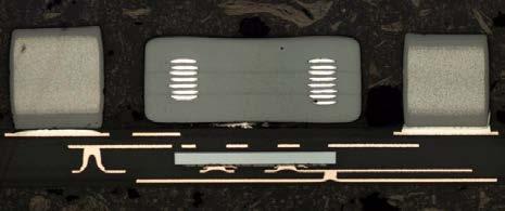
14 Example: FO-Packaging of a Multi-Sensor System TMV ASIC LGA pad sensor pressure sensor/asic package with thin film RDL Acceleration sensor/asic package with PCB based RDL and Through Mold Vias (TMV) for package stacking assembled sensor stack on test board Functional tests show sensor performance in specs

15 Roadmap Fan-Out Panel Level Packaging Source: Yole


16 PLPC Current Status performance f(l/s, pitch, no. dies,.) WL PL cost
17 Molding Compounds for Large Area Encapsulation Liquid Compression Molding Compounds Granular Compression Molding Compounds Sheet Lamination Molding Compounds Standard material for wafer level embedding Paste-like material is dispensed in the cavity and flows during tool closing and compression of the tooling Limited potential for large area due to complex dispense patterns needed and longer flow length? Standard material for MAP compression molding Granular material is distributed nearly homogeneously all over the cavity and melts and the droplets have to fuse during closing and compression of the tooling No limitations for large area application Standard material for wafer level embedding Material sheets are melting and only flow around dies for encapsulation Sheets in defined thicknesses/volume No limitations for large area application


18 Panel Mold Embedding Technologies Compression Molding Lamination Mold Tool Release Film Rubber Sheet Press Plate Release Film Cavity EMC Vacuum EMC Vacuum Mold Tool Wafer Rubber Sheet Reconfigured Wafer Standard process for MAP molding and WL mold embedding Use of liquid or granular compounds Tooling adapted to wafer size needed Thickness control by material weight Molding at constant temperature Typically an electro-mechanical press Current max. mold area: O/ 300 mm Standard process in PCB manufacturing Use of sheets is standard, use of granular or liquid compounds is feasible No expensive tooling needed Thickness control needed Lamination with temperature profile (heating/cooling) Typically a hydraulic press Current max. sheet size: 610x457 mm²
19 Compression Mold vs. Lamination - Press Profile Compression Molding Lamination Mold Tool Rubber Sheet Press Plate Release Film Release Film Cavity EMC Vacuum EMC Vacuum Rubber Sheet Reconfigured Wafer Mold Tool Wafer + PMC (+ PMC) 2 15 min min Short cycle time Constant temperature -> no heating or cooling ramps No full compression pressure over longer time PMC and mold release extra process steps Long cycle time, but multi-stack lamination is standard Heating or cooling ramps Full compression pressure over longer time PMC and mold release can be included
20 Panel Packaging Process Step Tasks To Solve Equipment Tape laminator Available automatic equipment? Pick and Place Accuracy on panel size? Material application Dispensing, sprinkle, Molding Uniformity, thickness control, Debonder Available automatic equipment? Lithography Stepper, laser ablation, LDI Sputtering, plating Thickness variation, lines & spaces Thinning & Dicing Available automatic equipment? carrier preparation assembly compression molding debonding redistribution handling, thinning & singulation Material Carrier steel, glass,..? Thermo release tape Alternatives? EMC liquid, granular, sheet? Dielectric polymers liquid or film? photosensitive or not? Sputter targets Plating Handling carrier Tape or other material Temporary adhesives Still a lot of open issues and questions


21 Embedding Technology - First Level Interconnection First level chip interconnection technologies inside a package: chip & wire flip chip chip embedding established smallest in 2D smallest in 3D

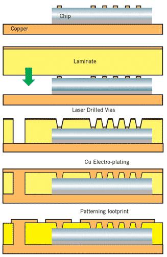
22 Power Electronics Packaging MOSFET wire-bonded power chips on DCB planar packages & module with embedded power chips Traditional Power modules Planar Power Packaging embedded MOSFET single module manufacturing large panel manufacturing low inductance high heat transfer high integration level high productivity
23 Power Embedding - Principle Features Completely planar conductors multiple wiring layers possible SMD assembly on top allows driver integration top side cooling possible very low parasitic effects Direct connection by Cu conductors / no bond wires high reliability by direct Cu to chip interconnects shielding capability Embedding of power chips into Printed Circuit Board structures cost saving by large area process Panel Level Packaging


24 Products DC/DC Converter SiPs 650 ma DC/DC converter System-in-Package with embedded chip volume manufacturing manufactured by manufactured by


25 Application Infineon Blade Technology SMD power package embedded Si MOSFET / Driver manufacturing on PCB format

26 Products GaN Power Chip Package courtesy AT&S/GaN Systems


27 Embedded Die Packages/Modules for different power classes Reduction in volume and form factor Low inductive interconnect to embedded die Improved electrical performance due to optimized switching behavior and reduced switching losses Improved reliability, active and passive testing 10kW+ Inverter modules 50W Schottky diode package 500W Pedelec Module


28 Embedded power components for electric vehicle applications Started in September 2013, duration 3 years Project goals: Industrialize double sided copper plating on wafer level Industrialize next generation automotive power modules Benefits: High performance power products with embedded MOSFET, IGBT, GaN, etc. Smallest form factor power supplies Partners: The European EmPower Project
29 Project EmPower - Demonstrators Diode Demonstrator double diode package 2 diodes embedded status: demonstrator realized, reliability tests ongoing 500 W Demonstrator pedelec inverter 24 V, 20 A 6 MOSFETs embedded control logic embedded in separate module status: demonstrator realized, reliability tests ongoing 50 kw Demonstrator automotive inverter 600 V, 200 A, 3 phases 24 IGBTs, 24 diodes embedded status: development ongoing


30 500 W Demonstrator Concept Embedded-logic Module ILFA SMD-logic Module ILFA Passives soldered on Power Core Continental IMS Top ILFA MOSFETs ST SMD-Layer Continental Power Core AT&S Adhesive Continental Cu Inlays AT&S IMS Bottom ILFA Solder process Conti Demonstrator-Assembly Conti Cu Inlay & MOSFET-Embedding AT&S IMS-Sintering TU Berlin


31 Sinter/Lamination Interconnection Cross Section IMS Powr Core IMS cross section of IMS/power core/ims sinter interconnects sinter connection die area sinter connection copper inlay area no large voids in Ag sinter interconnects

 of all")
32 Sinter Interconnects X-Ray Inspection X-ray of sintered top IMS / PowerCore / bottom IMS good alignment (± 50 µm) of all sintered layers
33 Concept 3D Stacking What is a 3D Power Stack? Stacking of Functional Layers by combined sinter/lamination technology controller driver I(O IGBT IGBT cooler controller IGBT driver cooler I/O IGBT
34 Concept 3D Stacking Stacking by combined sinter/lamination Process Flow Stacking of Functional Layers by combined sinter/lamination technology 1. stencil printing of Ag sinter paste on Functional Layer, paste drying 2. lay-up of prepreg sheet with opening for paste locations 3. lay-up of 2. Functional Layer on top, vacuum lamination at 3 MPa, 10 min./230 C, 60 min./200 C Result: a monolithic stack, thermally and electrically interconnected by high-reliable Ag joints, all gaps are filled by an isolating dielectric


35 Sinter/Lamination Interconnection FIB Analysis Cu Ag sinter layer Ag sinter layer Cu sufficiently low amount of micro voids in sinterde Ag (< 30 %)
36 Power Embedding Production and R&D MW R&D and Customer Projects Current (A) Blade Packages Production R&D Si R&D SiC Reihe1 Reihe2 Reihe3 1 Power Embedding products today DC/DC converter SiPs 0, Voltage (V)
37
38


39 MoMiCa Modular Camera Module Motivation to develop a miniaturized camera module with integrated image processing using PCB PLP embedding Potential Applications traffic lane recognition face / gender recognition
 256")
40 MoMiCa Camera Module Geometry 16 x 16 x 3.6 mm³, weight 2 g w/o lens PCB Layers construction 8 layer core with stacked mircrovias Embedded Components 32 bit microcontroller with image sensor interface (CogniVue CV2201 BGA 236 ) 256 Mbit Flash Memory (Macronix 8WSON MOSFET switch (IRF SOIC) USB ESD protection (NXP SOT457) 5 DC/DC-converters (Murata) oscillator 24 MHz (NXP 2 LEDs (0402) 34 capacitors (0201, 0603) 25 resistors (0201) 3 inductors (0603) Components on top 3 MPixel Image Sensor Omnivision 3642 lens CMT746 + lens holder 7 capacitors (0201) 1 resistor (0201) 1 inductor (0603) 1 microswitch

41 MoMiCa - Layer Sequence SMD Bildsensor 2 Lagen Kern Bauelemente 3 Build-up Lagen 2 Lagen Kern 3 Build-up Lagen Bauelemente Außenlage

42 MoMiCa Camera Module 3 Mpixel image sensor 32 bit microcontroller capacitor flash memory DC/DC converter Modular camera with integrated 32 bit image processor and memory


 1.")


43 Panel Level - Embedding Miniaturization Cost Electrical performance Source: Intel 1.5 Package Thickness (mm) 1.0 Ultra Thin core Coreless Die Embedding Panel level embedding: Time A platform for many applications Automotive, Medical Industrie 4.0, Robotik Internet of Things Consumer with improved reliability! RF-Modules Mobile Wireless Camera with image processing Trillion Sensor Vision X-ray of embedded µsd

44 Conclusions Panel-level Packaging will gain a significant market share There will be a fusion of different technologies FO WLP will evolve towards large panels PCB technology will evolve towards very high density... it just started - take the opportunity!

45 Thanks for your attention!
Towards Industrialization of Fan-out Panel Level Packaging
 Towards Industrialization of Fan-out Panel Level Packaging Tanja Braun S. Voges, O. Hölck, R. Kahle, S. Raatz, K.-F. Becker, M. Wöhrmann, L. Böttcher, M. Töpper, R. Aschenbrenner 1 Outline Introduction
System-in-Package (SiP) on Wafer Level, Enabled by Fan-Out WLP (ewlb)
 on Wafer Level, Enabled by Fan-Out WLP (ewlb)") System-in-Package (SiP) on Wafer Level, Enabled by Fan-Out WLP (ewlb) Steffen Kröhnert, José Campos, Eoin O Toole NANIUM S.A., Vila do Conde, Portugal Outline Short Company Overview NANIUM Introduction
System-in-Package (SiP) on Wafer Level, Enabled by Fan-Out WLP (ewlb) Steffen Kröhnert, José Campos, Eoin O Toole NANIUM S.A., Vila do Conde, Portugal Outline Short Company Overview NANIUM Introduction
Nanium Overview. Company Presentation
 Nanium Overview Company Presentation Nanium Overview Our name and logo nano prefix of Greek origin referring to small objects ium suffix of Latin origin that includes the formation of scientific terms
Challenges of Fan-Out WLP and Solution Alternatives John Almiranez
 Challenges of Fan-Out WLP and Solution Alternatives John Almiranez Advanced Packaging Business Development Asia Introduction to Fan-Out WLP Introduction World of mobile gadgetry continues to rapidly evolve
IME Technical Proposal. High Density FOWLP for Mobile Applications. 22 April High Density FOWLP Consortium Forum
 IME Technical Proposal High Density FOWLP for Mobile Applications 22 April 2014 Packaging driver for portable / mobile applications Key drivers/needs Smaller form-factor lower profile, substrate-less Higher
Thin Wafers Bonding & Processing
 Thin Wafers Bonding & Processing A market perspective 2012 Why New Handling Technologies Consumer electronics is today a big driver for smaller, higher performing & lower cost device configurations. These
3D Package Technologies Review with Gap Analysis for Mobile Application Requirements. Apr 22, 2014 STATS ChipPAC Japan
 3D Package Technologies Review with Gap Analysis for Mobile Application Requirements Apr 22, 2014 STATS ChipPAC Japan T.Nishio Contents Package trends and roadmap update Advanced technology update Fine
Challenges for Embedded Device Technologies for Package Level Integration
 Challenges for Embedded Device Technologies for Package Level Integration Kevin Cannon, Steve Riches Tribus-D Ltd Guangbin Dou, Andrew Holmes Imperial College London Embedded Die Technology IMAPS-UK/NMI
5. Packaging Technologies Trends
 5. Packaging Technologies Trends Electronic products and microsystems continue to find new applications in personal, healthcare, home, automotive, environmental and security systems. Advancements in packaging
Fan-Out Packaging Technologies and Markets Jérôme Azémar
 Fan-Out Packaging Technologies and Markets Jérôme Azémar Senior Market and Technology Analyst at Yole Développement Outline Advanced Packaging Platforms & Market drivers Fan-Out Packaging Principle & Definition
Challenges and Solutions for Cost Effective Next Generation Advanced Packaging. H.P. Wirtz, Ph.D. MiNaPAD Conference, Grenoble April 2012
 Challenges and Solutions for Cost Effective Next Generation Advanced Packaging H.P. Wirtz, Ph.D. MiNaPAD Conference, Grenoble April 2012 Outline Next Generation Package Requirements ewlb (Fan-Out Wafer
SEMI MEMS Tech Seminar (Sept 26, Cornaredo, Italy)
") SEMI MEMS Tech Seminar (Sept 26, 2013 - Cornaredo, Italy) Opportunities of Wafer Level Embedded Technologies for MEMS Devices T. Braun ( 1 ), K.-F. Becker ( 1 ), R. Kahle ( 2 ), V. Bader ( 1 ), S. Voges
SEMI MEMS Tech Seminar (Sept 26, 2013 - Cornaredo, Italy) Opportunities of Wafer Level Embedded Technologies for MEMS Devices T. Braun ( 1 ), K.-F. Becker ( 1 ), R. Kahle ( 2 ), V. Bader ( 1 ), S. Voges
Close supply chain collaboration enables easy implementation of chip embedded power SiP
 Close supply chain collaboration enables easy implementation of chip embedded power SiP Gerald Weidinger, R&D Project Leader, AT&S AT & S Austria Technologie & Systemtechnik Aktiengesellschaft Fabriksgasse13
Chips Face-up Panelization Approach For Fan-out Packaging
 Chips Face-up Panelization Approach For Fan-out Packaging Oct. 15, 2015 B. Rogers, D. Sanchez, C. Bishop, C. Sandstrom, C. Scanlan, TOlson T. REV A Background on FOWLP Fan-Out Wafer Level Packaging o Chips
Material based challenge and study of 2.1, 2.5 and 3D integration
 1 Material based challenge and study of 2.1, 2.5 and 3D integration Toshihisa Nonaka Packaging Solution Center R&D Headquarters Hitachi Chemical Co., Ltd., Sep. 8, 2016 Hitachi Chemical Co., Ltd. 2010.
Fraunhofer IZM. All Silicon System Integration Dresden Scope. M. Juergen Wolf
 Fraunhofer IZM All Silicon System Integration Dresden Scope M. Juergen Wolf Fraunhofer IZM All Silicon System Integration - ASSID Dresden, Berlin, Germany Fraunhofer IZM Focus of Activities Materials,
Development and Characterization of 300mm Large Panel ewlb (embedded Wafer Level BGA)
") Development and Characterization of 300mm Large Panel ewlb (embedded Wafer Level BGA) Seung Wook Yoon, Yaojian Lin and Pandi C. Marimuthu STATS ChipPAC Ltd. 5 Yishun Street 23, Singapore 768442 E-mail
Development and Characterization of 300mm Large Panel ewlb (embedded Wafer Level BGA) Seung Wook Yoon, Yaojian Lin and Pandi C. Marimuthu STATS ChipPAC Ltd. 5 Yishun Street 23, Singapore 768442 E-mail
Semiconductor IC Packaging Technology Challenges: The Next Five Years
 SPAY025 May 2006 White Paper Mario A. Bolanos, Director Semiconductor Group Packaging Technology Development, Texas Instruments In the era of communications and entertainment, growth of consumer electronics
First Demonstration of Panel Glass Fan-out (GFO) Packages for High I/O Density and High Frequency Multi-Chip Integration
 Packages for High I/O Density and High Frequency Multi-Chip Integration") 2017 IEEE 67th Electronic Components and Technology Conference First Demonstration of Panel Glass Fan-out (GFO) Packages for High I/O Density and High Frequency Multi-Chip Integration Tailong Shi, Chintan
2017 IEEE 67th Electronic Components and Technology Conference First Demonstration of Panel Glass Fan-out (GFO) Packages for High I/O Density and High Frequency Multi-Chip Integration Tailong Shi, Chintan
System in Package: Identified Technology Needs from the 2004 inemi Roadmap
 System in Package: Identified Technology Needs from the 2004 inemi Roadmap James Mark Bird Amkor Technology Inc System in package (SiP) technology has grown significantly in the past several years. It
IME Proprietary. EPRC 12 Project Proposal. 3D Embedded WLP. 15 th August 2012
 EPRC 12 Project Proposal 3D Embedded WLP 15 th August 2012 Motivation Factors driving IC market Higher density, lower cost, high yield Fan-out WLP/eWLP advantages Small footprint, low profile Low cost,
Innovative Substrate Technologies in the Era of IoTs
 Innovative Substrate Technologies in the Era of IoTs Dyi- Chung Hu 胡迪群 September 4, 2015 Unimicron Contents Introduction Substrate Technology - Evolution Substrate Technology - Revolution Glass substrate
Novel Materials and Activities for Next Generation Package. Hitachi Chemical., Co.Ltd. Packaging Solution Center Hiroaki Miyajima
 Novel Materials and Activities for Next Generation Package Hitachi Chemical., Co.Ltd. Packaging Solution Center Hiroaki Miyajima 1. Activities of Packaging Solution Center 2. Novel Materials for Next Gen.
Panel Discussion: Advanced Packaging
 Dr. Steve Bezuk Senior Director IC Packaging Engineering Qualcomm Technologies, Inc. Panel Discussion: Advanced Packaging PAGE 1 Technical Challenges of Packaging (Mobile Focus) Materials Die materials
Henkel Enabling Materials for Semiconductor and Sensor Assembly. TechLOUNGE, 14 November 2017
 Henkel Enabling Materials for Semiconductor and Sensor Assembly TechLOUNGE, 14 November 2017 Content Brief HENKEL Introduction and ELECTRONICS Focus Areas Innovative Semiconductor and Sensor Assembly Solutions
Fraunhofer IZM Bump Bonding and Electronic Packaging
 Fraunhofer IZM Bump Bonding and Electronic Packaging Fraunhofer Institute for Reliability and Microintegration (IZM) Gustav-Meyer-Allee 25 13355 Berlin Germany Dipl.-Ing. Thomas Fritzsch Contact: thomas.fritzsch@izm.fraunhofer.de
FABRICATION AND RELIABILITY OF ULTRA-FINE RDL STRUCTURES IN ADVANCED PACKAGING BY EXCIMER LASER ABLATION
 FABRICATION AND RELIABILITY OF ULTRA-FINE RDL STRUCTURES IN ADVANCED PACKAGING BY EXCIMER LASER ABLATION NCCAVS Joint Users Group Technical Symposium San Jose, June 7 th, 2017 Markus Arendt, SÜSS MicroTec
Henkel Adhesive Solutions for SiP Packaging. October 17-19, 2018 Shanghai, China
 Henkel Adhesive Solutions for SiP Packaging October 17-19, 2018 Shanghai, China Agenda 1 2 3 4 Overview: Henkel Adhesive Electronics Semiconductor Market Trends & SiP Drivers Henkel Adhesive Solutions
Power Electronics Packaging Solutions for Device Junction Temperature over 220 o C
 EPRC 12 Project Proposal Power Electronics Packaging Solutions for Device Junction Temperature over 220 o C 15 th August 2012 Page 1 Motivation Increased requirements of high power semiconductor device
Cost effective 300mm Large Scale ewlb (embedded Wafer Level BGA) Technology
 Technology") Cost effective 300mm Large Scale ewlb (embedded Wafer Level BGA) Technology by Meenakshi Prashant, Seung Wook Yoon, Yaojian LIN and Pandi C. Marimuthu STATS ChipPAC Ltd. 5 Yishun Street 23, Singapore 768442
Cost effective 300mm Large Scale ewlb (embedded Wafer Level BGA) Technology by Meenakshi Prashant, Seung Wook Yoon, Yaojian LIN and Pandi C. Marimuthu STATS ChipPAC Ltd. 5 Yishun Street 23, Singapore 768442
ewlb (embedded Wafer Level BGA) Technology: Next Generation 3D Packaging Solutions
 Technology: Next Generation 3D Packaging Solutions") ewlb (embedded Wafer Level BGA) Technology: Next Generation 3D Packaging Solutions by Seung Wook Yoon and Meenakshi Padmanathan STATS ChipPAC Ltd. Seungwook.yoon@statschippac.com Andreas Bahr Infineon
ewlb (embedded Wafer Level BGA) Technology: Next Generation 3D Packaging Solutions by Seung Wook Yoon and Meenakshi Padmanathan STATS ChipPAC Ltd. Seungwook.yoon@statschippac.com Andreas Bahr Infineon
Wire-Bond CABGA A New Near Die Size Packaging Innovation Yeonho Choi February 1, 2017
 Amkor Technology, Inc. White Paper Wire-Bond CABGA A New Near Die Size Packaging Innovation Yeonho Choi February 1, 2017 Abstract Expanding its ChipArray Ball Grid Array (CABGA) package form factor miniaturization
FRAUNHOFER INSTITUTE FOR RELIABILITY AND MICROINTEGRATION IZM DEPARTMENT WAFER LEVEL SYSTEM INTEGRATION BERLIN
 FRAUNHOFER INSTITUTE FOR RELIABILITY AND MICROINTEGRATION IZM DEPARTMENT WAFER LEVEL SYSTEM INTEGRATION BERLIN WAFER LEVEL SYSTEM INTEGRATION ELECTRONIC PACKAGING AT FRAUNHOFER IZM The Fraunhofer Institute
Chapter 4 Fabrication Process of Silicon Carrier and. Gold-Gold Thermocompression Bonding
 Chapter 4 Fabrication Process of Silicon Carrier and Gold-Gold Thermocompression Bonding 4.1 Introduction As mentioned in chapter 2, the MEMs carrier is designed to integrate the micro-machined inductor
TechARENA Packaging Exhibitor Session OCT/08, 2014 New WLP-Technology-Fusion Concept Steffen Kröhnert, Director of Technology, NANIUM S.A. V1.
 TechARENA Packaging Exhibitor Session OCT/08, 2014 New WLP-Technology-Fusion Concept Steffen Kröhnert, Director of Technology, NANIUM S.A. V1.0 EXT Notification NANIUM is highly committed to IP protection.
TSV Processing and Wafer Stacking. Kathy Cook and Maggie Zoberbier, 3D Business Development
 TSV Processing and Wafer Stacking Kathy Cook and Maggie Zoberbier, 3D Business Development Outline Why 3D Integration? TSV Process Variations Lithography Process Results Stacking Technology Wafer Bonding
RF System in Packages using Integrated Passive Devices
 RF System in Packages using Integrated Passive Devices by Kai Liu, YongTaek Lee, HyunTai Kim, Gwang Kim, and Billy Ahn STATS ChipPAC 1711 W. Greentree Drive, Suite #117, Tempe, AZ 85284, USA Tel: 480-222-1722
Between 2D and 3D: WLFO Packaging Technologies and Applications
 Between 2D and 3D: WLFO Packaging Technologies and Applications Minghao Shen Altera (now part of Intel) June 9 th, 2016 TFUG/CMPUG 3D Packaging Meeting Outline The 2.n D WLFO technologies Process and architect
IMPLEMENTATION OF A FULLY MOLDED FAN-OUT PACKAGING TECHNOLOGY
 IMPLEMENTATION OF A FULLY MOLDED FAN-OUT PACKAGING TECHNOLOGY B. Rogers, C. Scanlan, and T. Olson Deca Technologies, Inc. Tempe, AZ USA boyd.rogers@decatechnologies.com ABSTRACT Fan-Out Wafer-Level Packaging
Panel Fan-Out Manufacturing Why, When, and How?
 Panel Fan-Out Manufacturing Why, When, and How? Steffen Kroehnert, NANIUM S.A. Director of Technology Avenida Primeiro de Maio 801, 4485-629 Vila do Conde, Portugal IEEE 67 th ECTC Orlando, FL, USA IEEE
Hot Chips: Stacking Tutorial
 Hot Chips: Stacking Tutorial Choon Lee Technology HQ, Amkor Enabling a Microelectronic World Mobile Phone Technology Change Feature Phone Smartphone Smartphones as a Percentage of All Phones Source : The
ECE414/514 Electronics Packaging Spring 2012 Lecture 2. Lecture Objectives
 ECE414/514 Electronics Packaging Lecture 2 James E. Morris Dept of Electrical & Computer Engineering Portland State University Lecture Objectives Introduce first-level interconnect technologies: wire-bond,
Outline. Market Size Industry Trends Material Segment Trends China Summary. Packaging Materials Market Trends, Issues and Opportunities
 Packaging Materials Market Trends, Issues and Opportunities Dan Tracy Sr. Director Industry Research SEMI 8 th December 2015 Outline Market Size Industry Trends Material Segment Trends China Summary 1
SLIM TM, High Density Wafer Level Fan-out Package Development with Submicron RDL
 2017 IEEE 67th Electronic Components and Technology Conference SLIM TM, High Density Wafer Level Fan-out Package Development with Submicron RDL YoungRae Kim 1, JaeHun Bae 1, MinHwa Chang 1, AhRa Jo 1,
Cu Pillar Interconnect and Chip-Package-Interaction (CPI) for Advanced Cu Low K chip
 for Advanced Cu Low K chip") EPRC 12 Project Proposal Cu Pillar Interconnect and Chip-Package-Interaction (CPI) for Advanced Cu Low K chip 15 th Aug 2012 Page 1 Introduction: Motivation / Challenge Silicon device with ultra low k
EPRC 12 Project Proposal Cu Pillar Interconnect and Chip-Package-Interaction (CPI) for Advanced Cu Low K chip 15 th Aug 2012 Page 1 Introduction: Motivation / Challenge Silicon device with ultra low k
3D Wirebondless IGBT Module for High Power Applications Dr. Ziyang GAO Jun. 20, 2014
 3D Wirebondless IGBT Module for High Power Applications Dr. Ziyang GAO Jun. 20, 2014 1 1 Outline Background Information Technology Development Trend Technical Challenges ASTRI s Solutions Concluding Remarks
Cu electroplating in advanced packaging
 Cu electroplating in advanced packaging March 12 2019 Richard Hollman PhD Principal Process Engineer Internal Use Only Advancements in package technology The role of electroplating Examples: 4 challenging
Embedding Passive and Active Components: PCB Design and Fabrication Process Variations
 Embedding Passive and Active Components: PCB Design and Fabrication Process Variations Vern Solberg Solberg Technical Consulting Saratoga, California USA Abstract Embedding components within the PC board
Narrowing the Gap between Packaging and System
 Narrowing the Gap between Packaging and System Meptec Symposium 2015 ASE (US) Inc Ou Li Nov 10 th, 2015 Outline Industry Dynamics The Need for System Integrators IC/Pkg/System Collaboration Summary 2 Market
Design and Assembly Process Implementation of 3D Components
 IPC-7091 Design and Assembly Process Implementation of 3D Components Developed by the 3-D Electronic Packages Subcommittee (B-11) of the Packaged Electronic Components Committee (B-10) of IPC Users of
Glass Carrier for Fan Out Panel Level Package
 January 25, 2018 NEWS RELEASE Development of HRDP TM Material for Formation of Ultra-Fine Circuits with Glass Carrier for Fan Out Panel Level Package - Aiming for mass production in collaboration with
Thales vision & needs in advanced packaging for high end applications
 Thales vision & needs in advanced packaging for high end applications M. Brizoux, A. Lecavelier Thales Global Services / Group Industry Chemnitzer Seminar June 23 th -24 th, 2015 Fraunhofer ENAS - Packaging
Next Gen Packaging & Integration Panel
 Next Gen Packaging & Integration Panel ECTC 2012 Daniel Tracy, Sr. Director Industry Research & Statistics SEMI May 29, 2012 Packaging Supply Chain Market Trends Material Needs and Opportunities Market
Wafer Level Molded DDFN Package Project Duane Wilcoxen
 Wafer Level Molded DDFN Package Project Duane Wilcoxen Definition of DDFN (Encapsulated CSP) DDFN package basically is a CSP device with an epoxy coating on all (or most) of the device sides for added
Copyright 2009 Year IEEE. Reprinted from 2009 Electronic Components and Technology Conference. Such permission of the IEEE does not in any way imply
 Copyright 2009 Year IEEE. Reprinted from 2009 Electronic Components and Technology Conference. Such permission of the IEEE does not in any way imply IEEE endorsement of any of Institute of Microelectronics
3DIC Integration with TSV Current Progress and Future Outlook
 3DIC Integration with TSV Current Progress and Future Outlook Shan Gao, Dim-Lee Kwong Institute of Microelectronics, A*STAR (Agency for Science, Technology and Research) Singapore 9 September, 2010 1 Overview
A Flexible Vertical MEMs Probe Card Technology for Pre-Bump and ewlp Applications
 June 12 to 15, 2011 San Diego, CA A Flexible Vertical MEMs Probe Card Technology for Pre-Bump and ewlp Applications Mike Slessor Rick Marshall (MicroProbe, Inc.) Vertical MEMS for Pre-Bump Probe Introduction:
The Development of a Novel Stacked Package: Package in Package
 The Development of a Novel Stacked Package: Package in Package Abstract Stacked die Chip Scale Packages (CSPs) or Fine-pitch BGAs (FBGAs) have been readily adopted and integrated in many handheld products,
Design for Flip-Chip and Chip-Size Package Technology
 Design for Flip-Chip and Chip-Size Package Technology Vern Solberg Solberg Technology Consulting Madison, Wisconsin Abstract As new generations of electronic products emerge they often surpass the capability
Packaging Technologies Overview Dedicated to HEP Applications TWEPP 2018 Antwerp September the 21st,
 Packaging Technologies Overview Dedicated to HEP Applications TWEPP 2018 Antwerp September the 21st, 2018 stephane.bellenger@eolane.com Presentation Summary Main packaging challenges for High Energy Physics
Electrical and Fluidic Microbumps and Interconnects for 3D-IC and Silicon Interposer
 Electrical and Fluidic Microbumps and Interconnects for 3D-IC and Silicon Interposer Li Zheng, Student Member, IEEE, and Muhannad S. Bakir, Senior Member, IEEE Georgia Institute of Technology Atlanta,
The 3D Silicon Leader
 The 3D Silicon Leader TSV technology embedding high density capacitors for advanced 3D packaging solutions IMAPS Device Packaging Conference 2014 Catherine Bunel 2014.03.12 Outline Introduction IPDiA s
Silicon Interposers with Integrated Passive Devices: Ultra-Miniaturized Solution using 2.5D Packaging Platform
 Minapad 2014, May 21 22th, Grenoble; France Silicon Interposers with Integrated Passive Devices: Ultra-Miniaturized Solution using 2.5D Packaging Platform Stéphane Bellenger, Laëtitia Omnès, Jean-René
NXP SCM-i.MX6 Quad High Density Fan-Out Wafer-Level System-in-Package
 NXP SCM-i.MX6 Quad High Density Fan-Out Wafer-Level System-in-Package The first ultra-small multi-die low power module with boot memory and power management integrated in a package-on-package compatible
AN ANALYSIS OF KEY COST AND YIELD DRIVERS FOR FAN-OUT WAFER LEVEL PACKAGING
 AN ANALYSIS OF KEY COST AND YIELD DRIVERS FOR FAN-OUT WAFER LEVEL PACKAGING Amy Palesko SavanSys Solutions LLC Austin, TX, USA amyp@savansys.com ABSTRACT Although interest in wafer level packaging has
2.5D and 3D Semiconductor Package Technology: Evolution and Innovation
 2.5D and 3D Semiconductor Package Technology: Evolution and Innovation Vern Solberg Solberg Technical Consulting Saratoga, California USA Abstract The electronics industry is experiencing a renaissance
Package Solutions and Innovations
 Package Solutions and Innovations with Compression Molding IEEE SVC CPMT Aug 2015 Presented by C.H. Ang Towa USA Company Profile www.cpmt.org/scv 1 Corporate Overview Company: Towa Corp., Kyoto Japan Established:
Increasing challenges for size and cost reduction,
 Packageon-Package: The Story Behind This Industry Hit Package-onpackage (PoP) technology is rapidly evolving to keep pace with the demand for faster, higherdensity devices in smaller, thinner stacks. As
Assembly Reliability of TSOP/DFN PoP Stack Package
 As originally published in the IPC APEX EXPO Proceedings. Assembly Reliability of TSOP/DFN PoP Stack Package Reza Ghaffarian, Ph.D. Jet Propulsion Laboratory, California Institute of Technology Pasadena,
Flexible Substrates for Smart Sensor Applications
 Flexible Substrates for Smart Sensor Applications A novel approach that delivers miniaturized, hermetic, biostable and highly reliable smart sensor modules. AUTHORS Dr. Eckardt Bihler, Dr. Marc Hauer,
S/C Packaging Assembly Challenges Using Organic Substrate Technology
 S/C Packaging Assembly Challenges Using Organic Substrate Technology Presented by Bernd Appelt ASE Group Nov. 17, 2009 Overview The Packaging Challenge Chip Substrate Interactions Stiffeners for FC-BGA
3D-WLCSP Package Technology: Processing and Reliability Characterization
 3D-WLCSP Package Technology: Processing and Reliability Characterization, Paul N. Houston, Brian Lewis, Fei Xie, Ph.D., Zhaozhi Li, Ph.D.* ENGENT Inc. * Auburn University ENGENT, Inc. 2012 1 Outline Packaging
Graser User Conference Only
 2.5D/3D Design Solution Eric Chen & Scott Liu 31/Oct/2014 Roadmap data is provided for informational purposes only and does not represent a commitment to deliver any of the features or functionality discussed
Packaging Technologies for SiC Power Modules
 Packaging Technologies for SiC Power Modules Masafumi Horio Yuji Iizuka Yoshinari Ikeda ABSTRACT Wide bandgap materials such as silicon carbide (SiC) and gallium nitride (GaN) are attracting attention
ALTERNATIVES TO SOLDER IN INTERCONNECT, PACKAGING, AND ASSEMBLY
 ALTERNATIVES TO SOLDER IN INTERCONNECT, PACKAGING, AND ASSEMBLY Herbert J. Neuhaus, Ph.D., and Charles E. Bauer, Ph.D. TechLead Corporation Portland, OR, USA herb.neuhaus@techleadcorp.com ABSTRACT Solder
Advanced 3D ewlb PoP (embedded Wafer Level Ball Grid Array Package on Package) Technology
 Technology") Advanced 3D ewlb PoP (embedded Wafer Level Ball Grid Array Package on Package) Technology by Kang Chen, Jose Alvin Caparas, Linda Chua, Yaojian Lin and *Seung Wook Yoon STATS ChipPAC Ltd. 5 Yishun Street
Advanced 3D ewlb PoP (embedded Wafer Level Ball Grid Array Package on Package) Technology by Kang Chen, Jose Alvin Caparas, Linda Chua, Yaojian Lin and *Seung Wook Yoon STATS ChipPAC Ltd. 5 Yishun Street
The 3D Silicon Leader. Company Presentation. SMTA Houston, 14th March 2013
 The 3D Silicon Leader Company Presentation SMTA Houston, 14th March 2013 Who are we? Independent Company located in Caen, Normandy, France Dedicated to manufacturing of leading edge Integrated Passive
Comparison of topside contact layouts for power dies embedded in PCB
 1 / 23 Comparison of topside contact layouts for power dies embedded in PCB ESTC 2016, Grenoble Chenjiang YU 1, Cyril BUTTAY 2, Éric LABOURÉ 1, Vincent BLEY 3, Céline COMBETTES 3, Gilles BRILLAT 3 1 GEEPS,
Ultra Fine Pitch Bumping Using e-ni/au and Sn Lift-Off Processes
 Ultra Fine Pitch Bumping Using e-ni/au and Sn Lift-Off Processes Andrew Strandjord, Thorsten Teutsch, and Jing Li Pac Tech USA Packaging Technologies, Inc. Santa Clara, CA USA 95050 Thomas Oppert, and
TSV CHIP STACKING MEETS PRODUCTIVITY
 TSV CHIP STACKING MEETS PRODUCTIVITY EUROPEAN 3D TSV SUMMIT 22-23.1.2013 GRENOBLE HANNES KOSTNER DIRECTOR R&D BESI AUSTRIA OVERVIEW Flip Chip Packaging Evolution The Simple World of C4 New Flip Chip Demands
Fan-out Wafer Level ewlb Technology as an Advanced System-in- Package Solution
 Fan-out Wafer Level ewlb Technology as an Advanced System-in- Package Solution by Jacinta Aman Lim and Vinayak Pandey, STATS ChipPAC, Inc. Aung Kyaw Oo, Andy Yong, STATS ChipPAC Pte. Ltd. Originally published
iniaturization of medical devices thanks to flexible substrates ISO 9001 certified
 iniaturization of medical devices thanks to flexible substrates 04-12-2012 Hightec MC Presentation 2 Medical industry is clearly and urgently in need of the development of advanced interconnection solutions
Technical Viability of Stacked Silicon Interconnect Technology
 Technical Viability of Stacked Silicon Interconnect Technology Dr. Handel H. Jones Founder and CEO, IBS Inc. Los Gatos, California October 2010 TECHNICAL VIABILITY OF STACKED SILICON INTERCONNECT TECHNOLOGY
Credit Suisse Technology Conference
 Credit Suisse Technology Conference November 2007 Oleg Khaykin Ken Joyce Jim Fusaro EVP & COO Chief Administrative Officer Corporate VP, Wire Bond Products Forward Looking Statement Disclaimer All information
Basic PCB Level Assembly Process Methodology for 3D Package-on-Package
 Basic PCB Level Assembly Process Methodology for 3D Package-on-Package Vern Solberg STC-Madison Madison, Wisconsin USA Abstract The motivation for developing higher density IC packaging continues to be
Molding materials performances experimental study for the 3D interposer scheme
 Minapad 2014, May 21 22th, Grenoble; France Molding materials performances experimental study for the 3D interposer scheme Y. Sinquin, A. Garnier, M. Argoud, A. Jouve, L. Baud, J. Dechamp, N. Allouti,
3D & 2½D Test Challenges Getting to Known Good Die & Known Good Stack
 1 3D & 2½D Test Challenges Getting to Known Good Die & Known Good Stack Advantest Corporation 2 The final yield Any Multi-die Product Must Consider the Accumulated Yield Assume Test Can Provide 99% Die
Flip Chip - Integrated In A Standard SMT Process
 Flip Chip - Integrated In A Standard SMT Process By Wilhelm Prinz von Hessen, Universal Instruments Corporation, Binghamton, NY This paper reviews the implementation of a flip chip product in a typical
Two Chips Vertical Direction Embedded Miniaturized Package
 Two Chips Vertical Direction Embedded Miniaturized Package Shunsuke Sato, 1 Koji Munakata, 1 Masakazu Sato, 1 Atsushi Itabashi, 1 and Masatoshi Inaba 1 Continuous efforts have been made to achieve seemingly
Failure Modes in Wire bonded and Flip Chip Packages
 Failure Modes in Wire bonded and Flip Chip Packages Mumtaz Y. Bora Peregrine Semiconductor San Diego, Ca. 92121 mbora@psemi.com Abstract The growth of portable and wireless products is driving the miniaturization
Board Level Reliability Improvement in ewlb (Embedded Wafer Level BGA) Packages
 Packages") Board Level Reliability Improvement in ewlb (Embedded Wafer Level BGA) Packages by Seng Guan Chow, Yaojian Lin, Bernard Adams * and Seung Wook Yoon** STATS ChipPAC Ltd. 5 Yishun Street 23, Singapore 768442
Board Level Reliability Improvement in ewlb (Embedded Wafer Level BGA) Packages by Seng Guan Chow, Yaojian Lin, Bernard Adams * and Seung Wook Yoon** STATS ChipPAC Ltd. 5 Yishun Street 23, Singapore 768442
II. A. Basic Concept of Package.
 Wafer Level Package for Image Sensor Module Won Kyu Jeung, Chang Hyun Lim, Jingli Yuan, Seung Wook Park Samsung Electro-Mechanics Co., LTD 314, Maetan3-Dong, Yeongtong-Gu, Suwon, Gyunggi-Do, Korea 440-743
FOR SEMICONDUCTORS 2007 EDITION
 INTERNATIONAL TECHNOLOGY ROADMAP FOR SEMICONDUCTORS 2007 EDITION ASSEMBLY AND PACKAGING THE ITRS IS DEVISED AND INTENDED FOR TECHNOLOGY ASSESSMENT ONLY AND IS WITHOUT REGARD TO ANY COMMERCIAL CONSIDERATIONS
3D-IC Integration using D2C or D2W Alignment Schemes together with Local Oxide Reduction
 3D-IC Integration using D2C or D2W Alignment Schemes together with Local Oxide Reduction Gilbert Lecarpentier*, Jean-Stéphane Mottet* SET S.A.S. (Smart Equipment Technology), 131 Impasse Barteudet, 74490
Figure 1 Embedded Active and Passive Module (EMAP) Cross-section Schematic
 Cross-section Schematic") Super High Density Two Metal Layer Ultra-Thin Organic Substrates for Next Generation System-On-Package (SOP), SIP and Ultra-Fine Pitch Flip-Chip Packages Venky Sundaram, Hunter Chan, Fuhan Liu, and Rao
Super High Density Two Metal Layer Ultra-Thin Organic Substrates for Next Generation System-On-Package (SOP), SIP and Ultra-Fine Pitch Flip-Chip Packages Venky Sundaram, Hunter Chan, Fuhan Liu, and Rao
Development of Novel High Density System Integration Solutions in FOWLP Complex and Thin Wafer-Level SiP and Wafer-Level 3D Packages
 2017 IEEE 67th Electronic Components and Technology Conference Development of Novel High Density System Integration Solutions in FOWLP Complex and Thin Wafer-Level SiP and Wafer-Level 3D Packages André
Pouzdření pro moderní elektronické aplikace. Ing. Jiří Starý, SMT Plus. 17. října 2011
 Pouzdření pro moderní elektronické aplikace Ing. Jiří Starý, SMT Plus 17. října 2011 1 Od čipu k pouzdru a aplikacím Obsah přednášky Cu Wire, Multi-row QFN, Stacked Die, Flip Chip CSP, Cu Pillar Conventional
Advanced Packaging Technologies Update
 Advanced Packaging Technologies Update Welcome to ASM Pacific Techno log y Limited ASM Pacific Technology Ltd. 2016 www.asmpacific. com Presentation outline Advance Packaging Technologies driving forces