High Rate low pressure PECVD for barrier and optical coatings
|
|
|
- Theresa Lynch
- 6 years ago
- Views:
Transcription


1 High Rate low pressure PECVD for barrier and optical coatings, Matthias Fahland, John Fahlteich, Björn Meyer, Steffen Straach, Nicolas Schiller

2 Outline Introduction PECVD New developments magpecvd arcpecv D Examples Optics Barrier Outlook

3 Plasma enhanced CVD PECVD? CVD chemical vapor deposition Layer growth by chemical reaction at surface Layer material delivered by chemical compound precursor Energy transforms precursor into reactive species Plasma energy is used within PECVD Several by-products H 2 O CO 2 other low-molecular compounds Additional reactive gas suppliable 3
4 Why PECVD? Low temperature process Use of sensitive substrates like polymers Performs in vacuum Clean environment Broad choice of pre cursors and reactive gases Wide range of process parameters Power Frequency Pressure... 4
5 Outline Introduction PECVD New developments magpecvd arcpecv D Examples Optics Barrier Outlook

")
6 Magnetron based PECVD magpecvd Low pressure CV D (0.3 3 Pa) Driven by pulsed DC magnetron High coating rates (up to 400 nm m/min) Proven long-term stability over 8 h 6


7 magpecvd W ell-established plasma source Proven feasibility for large area applications Tuneable layer composition 7


8 magpecvd DC sputtering One hardware dual magnetron targets gas inlets Two processes magpecvd reactive DC sputtering 8
 Driven by hollow cathode arc plasma Very high")

9 Hollow-cathode arc PECVD arcpecvd Low pressure CV D (0.1 5 Pa) Driven by hollow cathode arc plasma Very high coating rates (> 2000 nm m/min) Tuneable layer composition Combination with evaporation possible Organic modified coatings 9

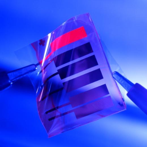
10 arcpecvd coating rates Linearly dependent from pre cursor flow Increase with plasma power Increase with additional reactive gas flow 10

11 Plasma syst em for arcpecvd Very high plasma density Commercially available Designed for production Any web width through numbers of plasma sources Developed for large area applications 2,85 m 11


12 arcpecvd Plasma enhanced evaporation One hardware hollow cathodes gas inlets Two processes arcpecvd Plasma enhanced reactive evaporation 12
13 Comparison of PECVD methods magpecvd arcpecv D HF-PECVD MW-PECVD typical frequency process pressure coating rates remarks khz bipolar pulsed DC MHz 2.45 GHz Pa Pa 1 20 Pa Pa nm m/min nm m/min industrially proven for wide webs, units commercially available nm m/min nm m/min pressure range different to PVD Low pressure CV D Inline combination with PVD possible 13
 magpecvd Evaporation")
14 Inline combination of PECVD and PVD R&D and pilot roll coater at FEP 600 mm coating width Multi-chamber design Available processes Sputtering (planar / rotatable) magpecvd Evaporation arcpecv D 14
15 Outline Introduction PECVD New developments magpecvd arcpecv D Examples Optics Barrier Outlook

16 Layer composition Precursor to reactive gas ratio adjustable Layer composition tunable HMDSO ratio low low carbon content inorganic SiO 2 -like layers HMDSO ratio high higher carbon content organic SiO x C y H z layers 16


17 Layer composition mechanical properties Increase HM DSO ratio Decrease of hardness Decrease of elastic modulus Increase in flexibility 17

18 Optical performance


19 Dielectric solar control layer st acks overall thickness approx nm SiO 2 made by infrared sputtering magpecvd 9 layers visible 19

20 Dielectric solar control layer st acks substrate curling due to layer stress nearly no layer stress 20

21 Dielectric UV-mirror with magpecvd 20 layers HfO 2 high refractive index 500 nm SiO 2 low refractive index high UV-reflectance high VIS-transmittance 21
22 Dielectric UV-mirror with magpecvd 20 layers Spectra measured across web width layer stack out of 20 single layers overall thickness approx nm highly uniform over 400 mm web width only 12 nm UV-edge shift across web width 22


23 Permeation barrier

24 Permeation barrier stacks Covering of layer defects by upper layers Surface smoothing Annealing of permeation barrier defects Increase of barrier performance Increase of mechanical robustness 400 nm 24


25 Permeation barrier stacks Inline made barrier stack 2 m/min web speed High barrier level comparable to single layers Improved mechanical robustness 25 Barrier 38 C, 90 % r.h. Sample size Ø100 mm

26 Permeation barrier st acks increased robustness Barrier layer Zinc-tin-oxid (ZTO) Interlayer SiO 2 made by magpecvd PECVD interlayers increase crack onset strain number of ZTO layers Layer stack more robust against mechanical deformation 26
27 Summary PECVD within multi-chamber PVD coaters Low pressure PECV D Designed for easy scale up Two options: magpecvd and arcpecv D One hardware multiple processes Optical coating stacks with nearly no layer stress Permeation barrier stacks with increased mechanical robustness Further development work Qualification for further pre cursors Adaptation to further industrial applications... Your application? Where can we work together? How can PECVD technology be integrated into your facilities? 27


28 Acknowledgement Essential results were obtained in several public projects, funded by Free State of Saxony, Federal Ministry of Education and Research and European Union 28
29 Thank you for your attention for barrier and optical coatings Fraunhofer FEP Winterbergstr Dresden Germany
From Vacuum to Atmosphere and back an in-house Process Chain for Different Products
 From Vacuum to Atmosphere and back an in-house Process Chain for Different Products Dr. Steffen Günther Vacuum coating low pressure 10-1 10-4 Pa (10-3 10-6 mbar) unhindered particle movement no unintended
Applied Research for Vacuum Web Coating: What is Coming Next?
 Applied Research for Vacuum Web Coating: What is Coming Next? Matthias Fahland, John Fahlteich, Steffen Günther, Manuela Junghähnel, Claus Luber, Nicolas Schiller, Cindy Steiner, Steffen Straach, Michiel
Roll-to-roll Technology for Transparent High Barrier Films
 Roll-to-roll Technology for Transparent High Barrier Films Presented at the AIMCAL Fall Technical Conference, October 19-22, 2008, Myrtle Beach, SC, USA Nicolas Schiller, John Fahlteich, Matthias Fahland,
Vacuum plasma treatment and coating of fluoropolymer webs challenges and applications
 Vacuum plasma treatment and coating of fluoropolymer webs challenges and applications AIMCAL 2016 Cindy Steiner John Fahlteich Dresden, 01.06.2016 page 1 Ethylene Tetrafluoroethylene (ETFE) semi-crystalline
New Dual Magnetron Plasma Source Designed For Large Area Substrate Pretreatment and Oxide Film Deposition P. Morse, R. Lovro, M. Rost, and J.
 New Dual Magnetron Plasma Source Designed For Large Area Substrate Pretreatment and Oxide Film Deposition P. Morse, R. Lovro, M. Rost, and J. German, Road Map Source Design Theory of Operation Experimental
1 Introduction. 2 Basic Technology
 Innovative Clear Barrier Technology for the Packaging Industry Nicolas Schiller 1, Steffen Straach, Steffen Günther Fraunhofer FEP, Germany Alexandra L. Quiceno G., Antonio García Contreras BIOFILM, Columbia
Plasma Activated EB-PVD of Titanium and its Compounds by Means of Large Area SAD
 AIMCAL 2005 Myrtle Beach, SC, USA, October 19th, 2005 Plasma Activated EB-PVD of Titanium and its Compounds by Means of Large Area SAD E. Reinhold, C. Steuer VON ARDENNE Anlagentechnik GmbH, Dresden, Germany
Photovoltaics & Solar Thermals. Thin-film equipment. Customized. FHR Anlagenbau GmbH I
 Photovoltaics & Solar Thermals Thin-film equipment. Customized. FHR Anlagenbau GmbH I www.fhr.de FHR Anlagenbau GmbH is an innovative enterprise in the branch of vacuum processing and thin-film technologies.
Advanced Glass Refinement by Thin Films - Trends and Challenges of Thin Film Technologies for Windows and Facade Glasses
 Advanced Glass Refinement by Thin Films - Trends and Challenges of Thin Film Technologies for Windows and Facade Glasses Dr.-Ing. Manuela Junghähnel Fraunhofer Institute for Elect ron Beam and Plasma Technology
Bringing Permeation Barrier Technology to Application. From Ultra-High Barrier Films to Functional Films for Flexible Electronics
 Bringing Permeation Barrier Technology to Application From Ultra-High Barrier Films to Functional Films for Flexible Electronics Degradation of organic devices on plastic films Barrier layer stack 1 1
Vacuum Deposition of High Performance Gas Barrier Materials for Electronics Applications
 Vacuum Deposition of High Performance Gas Barrier Materials for Electronics Applications Hélène Suttle DPhil Research Student Department of Materials -University of Oxford AIMCAL Fall Conference October
High Rate Deposition of Reactive Oxide Coatings by New Plasma Enhanced Chemical Vapor Deposition Source Technology
 General Plasma, Inc. 546 East 25th Street Tucson, Arizona 85713 tel. 520-882-5100 fax. 520-882-5165 High Rate Deposition of Reactive Oxide Coatings by New Plasma Enhanced Chemical Vapor Deposition Source
Electron beam technology for turbine coating
 Второй международный технологический форум "Инновации. Технологии. Производство." 23-25 марта 2015 года Electron beam technology for turbine coating Anastasiya Zagorni, MBA Prof. Dr. Christoph Metzner,
Advanced Sheet-to-Sheet and Roll-to-Roll thin-film processing on ultra-thin flexible glass for flexible electronic devices
 Advanced Sheet-to-Sheet and Roll-to-Roll thin-film processing on ultra-thin flexible glass for flexible electronic devices M. Junghaehnel 1, J. Westphalen 1, F. Naumann 2, G. Lorenz 2, M. Fahland 1, S.
Mass Production of Clear Barriers. Requirements on Vacuum Web Coaters for Quality Assurance. Rainer Ludwig, Applied Films, Alzenau, Germany.
 Mass Production of Clear Barriers Requirements on Vacuum Web Coaters for Quality Assurance Rainer Ludwig, Applied Films, Alzenau, Germany Abstract An increasing number of packages using Transparent Barrier
Gencoa Product Portfolio
 Gencoa offer the following range of products & process technology for the thin film industry developed over the last 20 years Planar Magnetrons Plasma Pre- Treaters Reactive Gas Controllers Gencoa Product
Ultra High Barrier Coatings by PECVD
 Society of Vacuum Coaters 2014 Technical Conference Presentation Ultra High Barrier Coatings by PECVD John Madocks & Phong Ngo, General Plasma Inc., 546 E. 25 th Street, Tucson, Arizona, USA Abstract Silicon
Improvement of gas barrier properties by combination of polymer film and gas barrier layer
 Improvement of gas barrier properties by combination of polymer film and gas barrier Y. Tsumagari, H. Murakami, K. Iseki and S. Yokoyama Toyobo Co., LTD. RESEARCH CENTER, - Katata 2-chome, Otsu, Shiga,
Metallization deposition and etching. Material mainly taken from Campbell, UCCS
 Metallization deposition and etching Material mainly taken from Campbell, UCCS Application Metallization is back-end processing Metals used are aluminum and copper Mainly involves deposition and etching,
Effective Closed-Loop Control for Reactive Sputtering Using Two Reactive Gases
 Effective Closed-Loop Control for Reactive Sputtering Using Two Reactive Gases D.C. Carter, W.D. Sproul, and D.J. Christie, Advanced Energy Industries, Inc., Fort Collins, CO Key Words: Reactive sputtering
Previous Lecture. Vacuum & Plasma systems for. Dry etching
 Previous Lecture Vacuum & Plasma systems for Dry etching Lecture 9: Evaporation & sputtering Objectives From this evaporation lecture you will learn: Evaporator system layout & parts Vapor pressure Crucible
Linear Plasma Sources for Surface Modification and Deposition for Large Area Coating
 Linear Plasma Sources for Surface Modification and Deposition for Large Area Coating Dr Tony Williams Gencoa Ltd, UK Victor Bellido-Gonzalez, Dr Dermot Monaghan, Dr Joseph Brindley, Robert Brown SVC 2016,
Vacuum plasma treatment and coating of fluoropolymer webs challenges and applications
 Vacuum plasma treatment and coating of fluoropolymer webs challenges and applications Cindy Steiner, John Fahlteich Fraunhofer Institute for Organic Electronics, Electron Beam and Plasma Technology FEP,
A Brief History of the Thermal Mass Flow Meter and Controller
 A Brief History of the Thermal Mass Flow Meter and Controller William J. Alvesteffer, William C. Baker, Randy Cole, and David C. Jacobs, Teledyne Hastings Instruments, Hampton, Virginia Chapter 18 from
PRECISION OPTICAL FILTERS BY EOSS - ENHANCED OPTICAL SPUTTERING SYSTEM. Fraunhofer
 PRECISION OPTICAL FILTERS BY EOSS - ENHANCED OPTICAL SPUTTERING SYSTEM EOSS ENHANCED OPTICAL SPUTTERING SYSTEM Fraunhofer IST, Braunschweig Contact: Dr. M. Vergöhl +49 531 2155 640 EOSS Coating System
Manipulation and control of spatial ALD layers for flexible devices. Aimcal Memphis 2016; Edward Clerkx
 Manipulation and control of spatial ALD layers for flexible devices Meyer Burger Netherlands Equipment manufacturer Functional inkjet printing Based in Eindhoven, the Netherlands Part of world-wide Meyer
Optical Coatings. Photonics 4 Luxury Coatings , Genève. Dr. Andreas Bächli Head of Optical Coatings at RhySearch, Buchs (SG)
") Optical Coatings Photonics 4 Luxury Coatings 21.06.2017, Genève Dr. Andreas Bächli Head of Optical Coatings at RhySearch, Buchs (SG) RhySearch The Research- and Innovation Center in the Rhine Valley RhySearch
Optical Coatings Photonics 4 Luxury Coatings 21.06.2017, Genève Dr. Andreas Bächli Head of Optical Coatings at RhySearch, Buchs (SG) RhySearch The Research- and Innovation Center in the Rhine Valley RhySearch
Lecture Day 2 Deposition
 Deposition Lecture Day 2 Deposition PVD - Physical Vapor Deposition E-beam Evaporation Thermal Evaporation (wire feed vs boat) Sputtering CVD - Chemical Vapor Deposition PECVD LPCVD MVD ALD MBE Plating
Progress in Roll-to-Roll Atomic Layer Deposition
 Progress in Roll-to-Roll Atomic Layer Deposition Council for Chemical Research Barrier Workshop Arlington, Virginia September 20, 2012 E. Dickey Lotus Applied Technology Outline ALD for barrier films ALD
Inline Sputtering System for Heterojunction Cells
 GENERIS PVD Inline Sputtering System for Heterojunction Cells GENERIS PVD Inline Sputter System for ITO and Ag Deposition on Heterojunction Solar Cells Sputtering Technology at a Glance has delivered far
PEAK EFFICIENCIES WITH FALLING MANUFACTURING COSTS
 PEAK EFFICIENCIES WITH FALLING MANUFACTURING COSTS Simple and cost-effective introduction of PERC technology into the mass production of solar cells Kerstin Strauch, Florian Schwarz, Sebastian Gatz 1 Introduction
Power Vision Ltd. PV Research. Power Vision Ltd. Unit R2, Herald Park, Crewe, Cheshire, CW1 6EA, UK Tel:
 Power Vision Ltd PV Research Power Vision Ltd Unit R2, Herald Park, Crewe, Cheshire, CW1 6EA, UK www.pvoptical.com Tel: +44 1270 253000 Flexible Whether it be fast AR coating onto temperature sensitive
ADDING VALUE TO VACUUM COATED PRODUCTS BY IMPROVING METALLIZED FILMS PROPERTIES AND FUNCTIONALITIES
 ADDING VALUE TO VACUUM COATED PRODUCTS BY IMPROVING METALLIZED FILMS PROPERTIES AND FUNCTIONALITIES by Fabiano Rimediotti NORMECCANICA GROUP Vacuum Division Piacenza Italy OUTLINE Introduction - Motivation
Large Area Coating for Glazing IOP Vacuum Symposium Daresbury 11 th Feb 2010
 Large Area Coating for Glazing IOP Vacuum Symposium Daresbury 11 th Feb 2010 Off-Line Coatings Technology Group Pilkington European Technology Centre 2 NSG Group Pilkington a member of NSG Group from June
Solar Selective Absorber Coating Methods Plasma Processes
 Solar Selective Absorber Coating Methods Plasma Processes Paul Gantenbein & Elimar Frank SPF - Institut für Solartechnik University of Applied Sciences Rapperswil (HSR) Optical properties of a selective
SPUTTERING TECHNOLOGY. for Multiple Applications such as Solar, Display, Semiconductor & 3D-Substrates
 SPUTTERING TECHNOLOGY for Multiple Applications such as Solar, Display, Semiconductor & 3D-Substrates 02 Over 20 Years of Know-how in Physical Vapor Deposition Sputtering PECVD Evaporation SINGULUS TECHNOLOGIES
Enabling new industries with high volume manufacturing: learnings from R2R processing in wearable and flexible displays
 Enabling new industries with high volume manufacturing: learnings from R2R processing in wearable and flexible displays Tobias Stolley, Technologist Applied Materials WEB Coating GmbH Industiral Technologies
EQUIPMENT EQUIPMENT FOR HIGH-EFFICIENCY SOLAR CONCEPTS CRYSTALLINE SILICON PV. SCALA XEA nova XENIA
 CRYSTALLINE SILICON PV EQUIPMENT EQUIPMENT FOR HIGH-EFFICIENCY SOLAR CONCEPTS SCALA XEA nova XENIA VON ARDENNE was founded in 1991 as a spin-off of the former Manfred von Ardenne Research Institute. The
Comparison of Different Sputter Processes for ITO: Planar DC versus Planar AC
 Comparison of Different Sputter Processes for ITO: Planar DC versus Planar AC P. Sauer, H.-G. Lotz, A. Hellmich, R. Kukla, J. Schröder Applied Films GmbH & Co. KG, Alzenau, Germany Key Words: ITO MF PET
Handbook Of Thin Film Deposition Processes And Techniques (materials And Processing Technology)
") Handbook Of Thin Film Deposition Processes And Techniques (materials And Processing Technology) R. Glang, in: Handbook of Thin Film Technology (L. I. Maissel and R. Glang, eds.) T. A. Delchar, Vacuum Physics
Handbook Of Thin Film Deposition Processes And Techniques (materials And Processing Technology) R. Glang, in: Handbook of Thin Film Technology (L. I. Maissel and R. Glang, eds.) T. A. Delchar, Vacuum Physics
Durable Neutral Color Anti-Reflective Coating for Mobile Displays
 Durable Neutral Color Anti-Reflective Coating for Mobile Displays By John Madocks and Phong Ngo, General Plasma, Inc. Figure 1: Samsung S4 with top half of cover glass coated with AR+DLC Abstract An in-line
AC Reactive Sputtering with Inverted Cylindrical Magnetrons
 AC Reactive Sputtering with Inverted Cylindrical Magnetrons D.A. Glocker, Isoflux Incorporated, Rush, NY; and V.W. Lindberg and A.R. Woodard, Rochester Institute of Technology, Rochester, NY Key Words:
Transparent Ultra-Barrier Film Production and Product Integration
 Transparent Ultra-Barrier Film Production and Product Integration Mark George, Martin Rosenblum, Jason Bloking Rex Chang Vitriflex Inc., 2350 Zanker Road, Suite 20, San Jose, CA 95131 Introduction Vitriflex
Productivity versus Profitability in Vacuum Web Coating
 Productivity versus Profitability in Vacuum Web Coating Liz Josephson, Applied Films Corp. Longmont CO Dirk Hoffmann, Gerard Loebig Applied Films GmbH & Co. KG, Alzenau, Germany Market requirements Quality
MODULAR PROCESS SYSTEMS ADVANCED COATING EQUIPMENT ADVANCED COATING EQUIPMENT
 MODULAR PROCESS SYSTEMS ADVANCED COATING EQUIPMENT MODULAR PROCESS SYSTEMS ADVANCED COATING EQUIPMENT APPLICATIONS VON ARDENNE is your partner of choice if you are looking for systems with a modular design
SINGULUS TECHNOLOGIES
 SINGULUS TECHNOLOGIES December 2013 Optical Coating Solutions - Applications and Technology Coating Solutions December 2013-2 - Agenda Coating History @SINGULUS Industry Requirements Coating Application,
Physical Vapor Deposition (PVD) Zheng Yang
 Zheng Yang") Physical Vapor Deposition (PVD) Zheng Yang ERF 3017, email: yangzhen@uic.edu Page 1 Major Fabrication Steps in MOS Process Flow UV light Mask oxygen Silicon dioxide photoresist exposed photoresist oxide
Physical Vapor Deposition (PVD) Zheng Yang ERF 3017, email: yangzhen@uic.edu Page 1 Major Fabrication Steps in MOS Process Flow UV light Mask oxygen Silicon dioxide photoresist exposed photoresist oxide
Improving the Performance of Ceramic Barrier Layers used in Packaging Materials
 Improving the Performance of Ceramic Barrier Layers used in Packaging Materials Roland Trassl Senior Manager Advanced Development Applied Materials WEB Coating GmbH AIMCAL Tampa, Florida, USA 18 th October,
Roll-to-roll ALD prototype for 500 mm wide webs
 Roll-to-roll ALD prototype for 500 mm wide webs Tapani Alasaarela, Mikko Söderlund, Pekka Soininen Beneq Oy, Ensimmäinen Savu, 01510 Vantaa, Finland Roll-to-roll (R2R) atomic layer deposition (ALD) technology
Development of Low-resistivity TiN Films using Cat Radical Sources
 Development of Low-resistivity TiN Films using Cat Radical Sources Masamichi Harada*, Yohei Ogawa*, Satoshi Toyoda* and Harunori Ushikawa** In Cu wiring processes in the 32-nm node generation or later,
Using a standard Penning Gauge as a powerful means of monitoring and feedback control
 Gencoa - Dermot Monaghan Using a standard Penning Gauge as a powerful means of monitoring and feedback control Victor Bellido-González, Sarah Powell, Benoit Daniel, John Counsell, Dermot Monaghan Structure
LOW PRESSURE PLASMA COATINGS FOR FOOD PACKAGING
 LOW PRESSURE PLASMA COATINGS FOR FOOD PACKAGING O. Kylian, J.Hanuš, O.Polonskyi, A. Choukourov, A. Shelemin, A. Kuzminova, D. Slavínká, L. Hanyková, H. Biederman Charles University in Prague Faculty of
GENERIS PVD. Inline Sputtering System for Heterojunction Solar Cells
 GENERIS PVD Inline Sputtering System for Heterojunction Solar Cells GENERIS PVD Inline Sputtering System for Heterojunction Solar Cells Sputtering Competence has delivered far more than 8000 vacuum sputtering
Ellipsometry as a tool for identifying process issues in roll-to-roll sputter deposited metal-oxide coatings
 Ellipsometry as a tool for identifying process issues in roll-to-roll sputter deposited metal-oxide coatings Sharon Louch Centre for Process Innovation, Wilton Centre, edcar. UK. TS10 3H Abstract Ellipsometry
High Performance Optical Coatings Deposited Using Closed Field Magnetron Sputtering
 High Performance Optical Coatings Deposited Using Closed Field Magnetron Sputtering D.R. Gibson, I.T. Brinkley, and J.L. Martin Applied Multilayers LLC, 1801 SE Commerce Avenue, Battle Ground, WA 98604
Nucleation and growth of nanostructures and films. Seongshik (Sean) Oh
 Oh") Nucleation and growth of nanostructures and films Seongshik (Sean) Oh Outline Introduction and Overview 1. Thermodynamics and Kinetics of thin film growth 2. Defects in films 3. Amorphous, Polycrystalline
Nucleation and growth of nanostructures and films Seongshik (Sean) Oh Outline Introduction and Overview 1. Thermodynamics and Kinetics of thin film growth 2. Defects in films 3. Amorphous, Polycrystalline
Nonplanar Metallization. Planar Metallization. Professor N Cheung, U.C. Berkeley
 Nonplanar Metallization Planar Metallization Passivation Metal 5 (copper) Metal 3 (copper) Interlevel dielectric (ILD) Via (tungsten) Metal 1 (copper) Tungsten Plug to Si Silicon Caps and Plugs oxide oxide
ALD of Copper and Copper Oxide Thin Films for Applications in Metallization Systems of ULSI Devices
 ALD of Copper and Copper Oxide Thin Films for Applications in Metallization Systems of ULSI Devices a, Steffen Oswald b, Nina Roth c, Heinrich Lang c, Stefan E. Schulz a,d, and Thomas Gessner a,d a Center
The Effects of Defects on the Moisture-Barrier Performance of Clear Coatings on Polymer Substrates.
 AIMCAL, CHARLESTON, SC, 2013 The Effects of Defects on the Moisture-Barrier Performance of Clear Coatings on Polymer Substrates. The National Centre for Printed Electronics ALF part SMITH of Centre for
An innovative approach to coatings on large optics
 An innovative approach to coatings on large optics OpTIC Strategic Conference 16 th -17 th November 2010 "Photographie: Philippe Bourgeois" CILAS - Établissement Marseille Z.I. St Mitre 15 avenue de la
 2007 PLACE Conference September 16-20 St Louis, MO Nano-Composite Polymer Optical Coatings Vampire Optical Coatings, Inc. Tom Faris vcoat@copper.net Introduction What is a nano-composite polymer coating?
and cost implications of corrosion, casting a spot light on the need for innovation in pipe coating materials and processes.
 A ccording to the Energy Information Administration s International Energy Outlook for 2006, world oil demand is expected to grow from 80 million barrels per day in 2003 to 98 million barrels per day in
Flexible functional devices at mass production level with the FLEx R2R sald platform
 Flexible functional devices at mass production level with the FLEx R2R sald platform D. Spee, W. Boonen, D. Borsa and E. Clerkx Meyer Burger (Netherlands) B.V. Meyer Burger Introduction to sald Challenges
Institute of Solid State Physics. Technische Universität Graz. Deposition. Franssila: Chapters 5 & 6. Peter Hadley
 Technische Universität Graz Institute of Solid State Physics Deposition Franssila: Chapters 5 & 6 Peter Hadley Silicon wafers Total Thickness Variation: a good 8" Prime wafer would be < 15 m Site flatness
CORIAL D500. Large capacity batch system for 24/7 production environment
 CORIAL D500 Large capacity batch system for 24/7 production environment High-quality films for a wide range of materials, incl. SiO2, Si3N4, SiOCH, SiOF, SiC and asi-h films Film deposition from 120 C
ITO SPUTTER COATED FILMS FOR TOUCH PANEL APPLICATIONS USING ROTARY SINTERED CERAMIC ITO TARGETS: WHAT CAN BE LEARNED FROM GLASS COATING?
 ITO SPUTTER COATED FILMS FOR TOUCH PANEL APPLICATIONS USING ROTARY SINTERED CERAMIC ITO TARGETS: WHAT CAN BE LEARNED FROM GLASS COATING? Paul Lippens AIMCAL Web coating conference 2012 Outline Introduction
Deposition of AlOx/SiN stack and SiN for high efficient bifacial PERC solar cells using only one deposition system MAiA 3in1
 SNEC PV Power Expo and Conference 2017 Deposition of AlOx/SiN stack and SiN for high efficient bifacial PERC solar cells using only one deposition system MAiA 3in1 E. Vetter 1, T. Grosse 1, H.P. Sperlich
Energy-efficient glazing
 Energy-efficient glazing Low-E solar reflective coatings Float glass is traditionally used in the building and automotive industries to provide both clear and tinted transparent barriers to the elements.
EE 5344 Introduction to MEMS. CHAPTER 3 Conventional Si Processing
 3. Conventional licon Processing Micromachining, Microfabrication. EE 5344 Introduction to MEMS CHAPTER 3 Conventional Processing Why silicon? Abundant, cheap, easy to process. licon planar Integrated
Corial D500 No mechanical cleaning
 Corial D500 No mechanical cleaning Large capacity batch system for 24/7 production environment High-quality films for a wide range of materials, incl. SiO2, Si3N4, SiOCH, SiOF, SiC and asi-h films Film
Barrier Coating Encapsulation Using Rotatable Cylindrical Sputtering Cathodes
 Barrier Coating Encapsulation Using Rotatable Cylindrical Sputtering Cathodes V. Bellido-Gonzalez, D. Monaghan, R. Brown, B. Daniel, J. Brindley, A. Azzopardi, and I. Sorzabal-Bellido, Gencoa Ltd., Liverpool,
Chapter 3 Silicon Device Fabrication Technology
 Chapter 3 Silicon Device Fabrication Technology Over 10 15 transistors (or 100,000 for every person in the world) are manufactured every year. VLSI (Very Large Scale Integration) ULSI (Ultra Large Scale
About Cambridge NanoTech Atomic Layer Deposition (ALD) Selected Applications Manufacturing Considerations ALD Reactors Summary
 Selected Applications Manufacturing Considerations ALD Reactors Summary") About Cambridge NanoTech Atomic Layer Deposition (ALD) Selected Applications Manufacturing Considerations ALD Reactors Summary Founded in 2003 by Dr. Jill Becker Located in Cambridge, MA Grew directly
About Cambridge NanoTech Atomic Layer Deposition (ALD) Selected Applications Manufacturing Considerations ALD Reactors Summary Founded in 2003 by Dr. Jill Becker Located in Cambridge, MA Grew directly
Vacuum Deposition of High Performance Gas Barrier Materials
 Vacuum Deposition of High Performance Gas Barrier Materials H. Suttle, A. J. Topping, & H. E. Assender Department of Materials, University of Oxford, Parks Road, Oxford OX1 3PH ABSTRACT High performance
AIMCAL R2R Conference
 Contents Introduction Markets OLED Structures Technology Fabrication Process Evaluation (Microstructure & etc) Summary Introduction [Merit of Rigid OLED Display] Cheap product cost Mass production Free
CONFERENCE EVALUATION FORM
 2015 AIMCAL Web Coating & Handling / SPE FlexPackCon CONFERENCE EVALUATION FORM To upgrade the quality of the Web Coating & Handling / FlexPackCon Conference, we would appreciate your comments. MONDAY,
Thermal Load And Heat Transfer Regarding EBPVD Of Plastic Web And Thin Metal Foils
 Thermal Load And Heat Transfer Regarding EBPVD Of Plastic Web And Thin Metal Foils J. Richter, E. Reinhold, Chr. Steuer VON ARDENNE Anlagentechnik GmbH D-01324 Dresden, Germany 1 - Thema - 12.08.2003 e-mail:
Microstructure of Electronic Materials. Amorphous materials. Single-Crystal Material. Professor N Cheung, U.C. Berkeley
 Microstructure of Electronic Materials Amorphous materials Single-Crystal Material 1 The Si Atom The Si Crystal diamond structure High-performance semiconductor devices require defect-free crystals 2 Crystallographic
PATTERNING OF OXIDE THIN FILMS BY UV-LASER ABLATION
 Journal of Optoelectronics and Advanced Materials Vol. 7, No. 3, June 2005, p. 1191-1195 Invited lecture PATTERNING OF OXIDE THIN FILMS BY UV-LASER ABLATION J. Ihlemann * Laser-Laboratorium Göttingen e.v.,
"Plasma CVD passivation; Key to high efficiency silicon solar cells",
 "Plasma CVD passivation; Key to high efficiency silicon solar cells", David Tanner Date: May 7, 2015 2012 GTAT Corporation. All rights reserved. Summary: Remarkable efficiency improvements of silicon solar
1 MARCH 2017 FILM DEPOSITION NANOTECHNOLOGY
 1 MARCH 2017 FILM DEPOSITION NANOTECHNOLOGY PRESENTATION Pedro C. Feijoo E-mail: PedroCarlos.Feijoo@uab.cat FABRICATION TECHNOLOGIES FOR NANOELECTRONIC DEVICES. PEDRO C. FEIJOO 2 FILM GROWTH Chemical vapor
Latest Development in Vacuum Metallisation
 Latest Development in Vacuum Metallisation Professor Nadir Ahmed Vacuum Metallising Consultant General Vacuum Equipment Ltd. Pennine Business Park, Pilsworth Road, Heywood OL10 2TL England Tel: +44(0)1706
ATOMIC LAYER DEPOSITION OF 2D TRANSITION METAL DICHALOGENIDES
 ATOMIC LAYER DEPOSITION OF 2D TRANSITION METAL DICHALOGENIDES Annelies Delabie, M. Caymax, B. Groven, M. Heyne, K. Haesevoets, J. Meersschaut, T. Nuytten, H. Bender, T. Conard, P. Verdonck, S. Van Elshocht,
Chapter 1. Introduction to Thin Film Technology
 Chapter 1. Introduction to Thin Film Technology Thin films are deposited onto bulk materials (substrates) to achieve properties unattainable or not easily attainable by substrates alone. How thin? 1 Properties:
Transparent Heat Mirror Using Plasma Polymer Fluorocarbon Fabricated by Continuous Roll-to-Roll Sputtering
 2R Conference USA 2018 Transparent Heat Mirror Using Plasma Polymer Fluorocarbon Fabricated by Continuous Roll-to-Roll Sputtering Sang-Jin Lee, Ph.D/Principal Researcher Sung Hyun Kim, Mac Kim, Tae-Woon
Be careful what you wish for
 Be careful what you wish for Four Point Probe Key measurement tool in microelectronics fabrication What is Four Point Probing Four Point Probing is a method for measuring the resistivity of a substance.
Review of CMOS Processing Technology
 - Scaling and Integration Moore s Law Unit processes Thin Film Deposition Etching Ion Implantation Photolithography Chemical Mechanical Polishing 1. Thin Film Deposition Layer of materials ranging from
BK 7 / H-K9L / B270. Description
 BK 7 / H-K9L / B270 Description BK7 produced by Schott and its equivalent H-K9L are used for standard optical glass components, or when optical glass is requested for customized items. BK7 and H- K9L are
Magnetron Sputter Cathodes planar & rotatable. Linear ion sources. Reactive gas controller & endpoint detector
 GENCOA products cover 3 sputtering related areas Magnetron Sputter Cathodes planar & rotatable Reactive gas controller & endpoint detector Linear ion sources Other activities include on-site process implementation,
Maximizing the Potential of Rotatable Magnetron Sputter Sources for Web Coating Applications
 Maximizing the Potential of Rotatable Magnetron Sputter Sources for Web Coating Applications V.Bellido-Gonzalez, Dermot Monaghan, Robert Brown, Alex Azzopardi, Gencoa, Liverpool UK Structure of presentation
Corial PS200 4-sided multi-module platform
 Corial PS200 4-sided multi-module platform Single wafer platform equipped with 200 mm modules Integration of ICP-CVD or PECVD process chambers Fully automated platform with cassette-to-cassette handler
PlasmaPro TM System100 & System133. Modular tools for wafer processing100
 TM System100 & System133 Modular tools for wafer processing100 System100 & System133 Plasma etch & deposition process modules Oxford Instruments System100 and System133 process modules are built on 200mm
Contents. 1. Introduction to Materials Processing Starting Materials 21. Acknowledgements
 Preface Acknowledgements xiii xv 1. Introduction to Materials Processing 1 1.1 Materials Processing: Definition and Scope 1 1.2 Three Approaches to Materials Processing 4 1.3 Materials Processing Steps
FIBRE-COUPLED HIGH-INDEX PECVD SILICON- OXYNITRIDE WAVEGUIDES ON SILICON
 FIBRE-COUPLED HIGH-INDEX PECVD SILICON- OXYNITRIDE WAVEGUIDES ON SILICON Maxim Fadel and Edgar Voges University of Dortmund, High Frequency Institute, Friedrich-Woehler Weg 4, 44227 Dortmund, Germany ABSTRACT
Ion-plasma technologies and equipment
 Ion-plasma technologies and equipment VACUUM ION-PLASMA INSTALLATIONS OF «OPAL» SERIES «Opal» series ion-plasma installations are designed for deposition of low-emission, reflective and toned coatings
Plasma Quest Limited
 Plasma Quest Limited A Remote Plasma Sputter Process for High Rate Web Coating of Low Temperature Plastic Film with High Quality Thin Film Metals and Insulators Dr. Peter Hockley and Prof. Mike Thwaites,
Czochralski Crystal Growth
 Czochralski Crystal Growth Crystal Pulling Crystal Ingots Shaping and Polishing 300 mm wafer 1 2 Advantage of larger diameter wafers Wafer area larger Chip area larger 3 4 Large-Diameter Wafer Handling
Activities in Plasma Process Technology at SENTECH Instruments GmbH, Berlin. Dr. Frank Schmidt
 Activities in Plasma Process Technology at SENTECH Instruments GmbH, Berlin Dr. Frank Schmidt The Company Company Private company, founded 1990 80 employees ISO 9001 Location Science & Technology Park,
Transactions on Engineering Sciences vol 2, 1993 WIT Press, ISSN
 A study of thin-film continuous coating process by vapour deposition P. Gimondo," F. Arezzo,* B. Grifoni,* G. Jasch& "Centra Sviluppo Materiali SpA, Via di Castel & Von Ardenne Anlagentchnik GmbH, Plattleite
Highly (200)-Preferred Orientation TiN Thin Films Grown by DC Reactive Magnetron Sputtering
-Preferred Orientation TiN Thin Films Grown by DC Reactive Magnetron Sputtering") American Journal of Physics and Applications 2017; 5(3): 41-45 http://www.sciencepublishinggroup.com/j/ajpa doi: 10.11648/j.ajpa.20170503.12 ISSN: 2330-4286 (Print); ISSN: 2330-4308 (Online) Highly (200)-Preferred
American Journal of Physics and Applications 2017; 5(3): 41-45 http://www.sciencepublishinggroup.com/j/ajpa doi: 10.11648/j.ajpa.20170503.12 ISSN: 2330-4286 (Print); ISSN: 2330-4308 (Online) Highly (200)-Preferred