ELECTRON MICROSCOPY FOR MULTI-SCALE POROUS MATERIALS PART II - TEM PRINCIPLES
|
|
|
- Corey Shepherd
- 6 years ago
- Views:
Transcription


1 ELECTRON MICROSCOPY FOR MULTI-SCALE POROUS MATERIALS PART II - TEM PRINCIPLES Marseille Winter School on Multi-Scale Porous Materials (Jan ) A. BARONNET
2 Principles of Transmission Electron Microscopy (TEM) The TEM machine - How it is made of and how it works - Attached techniques Imaging and diffraction Capabilities of the (Fast) Fourier Transform (FFT) in TEM Sample preparation techniques Some applications of high-resolution TEM on clay and clay-related materials -Structural characterization at atomic scale (T and O sheets, polytypes, mixed-layer silicates, non-planar serpentines) Other crystals with reduced dimensionnality: CSH, tunnel Mn oxides, Adding the chemical characterization to complete data ( Jérémie Berthonneau)

3 The electron microscope upside down a "light" microscope in which electrons replace photons vacuum torr Haute tension Kv

4 MET 200 kv (CRMCN)


5 Electron travels through the TEM
6 In a TEM, you may switch immediately from the direct space (image) to the reciprocal space (diffraction) crystal incident beam my god! the eternal dream of my life! objective lens back focal plane diffraction pattern image plane


7 1.25 MV HRTEM RUCA (Anvers) Bigger and bigger? Better and better? Image-corrected 300 kev HRTEM Aix-Marseille Université Desperate guy (red face)) trying to image antigorite


8 Electron sources and acceleration voltage Classical tungsten filament A LaB 6 tip cold and warm cathode field emission tip coherent beam acceleration voltage 300keV Best against beam damages not so coherent beam good for beam-sensitive minerals
9 Incident e Backscattered e (SEM/EBSD) Auger e X-rays(EDS) Cathodaluminescence Secondary e (SEM) Inelastically Scattered e (EELS) Elastically Scattered e (ED) Unscattered e (transmitted beam)

10 Sample volumes analyzed with Electron microprobe/ TEM EDS (ATEM) 5 µm Quantitative data for oxygen and above Z 16 X-ray energy 0-20keV V analyzed = 10 mm 3 V analyzed = 10-6 mm 3 ATEM is a satellite tool absolutely needed for mineralogical studies dealing with micro to nano size of crystals
11 An ideal sample to enter the TEM should be: : Transparent for standard acceleration ( kv) => 0 < thickness < 500 nm for oxides (silicates) HRTEM --> 5-10 nm Manipulable (support inscribed in diam. 3 mm) Conductive or rendered conductive by metallization => amorphous C-coating Representative of the bulk of the materials => structures, microstructures, defects, chemical compositions, be saved (preparation and observation)
12 The thin-sample preparation techniques which materials do you want to look at? organic, mineral, hard, soft, coherent, porous, granular, fibrous, composite,, hydroxylated, hydrated,... What do you want to see in this material? shape, size, crystallinity, chemical composition, defects, texture, ultrastructure,...

13 TEM grids and slots mesh grids conducting: Cu, Ni, Mo, Au,... "bivalve" grids 3 mm honeycomb grid "stadium" slot for ion thinning

")

14 The "drop deposition" technique 3 mm Advantages - the simplest and quickest -for powder characterization -(size, shape, diffraction, composition) Drawbacks -not for water soluble minerals -Particle density adjustment -drift and tilt under the beam (no clean HRTEM) - +-noise from C-film background(holey, lacey C-films- C-film wettability 1 mm Celadonite mica crystals (O. Grauby) synthetic chrysotile charge

15 Ultramicrotoming (continue) advantages unique for powders, fibers, synthesis charges chemically extremely clean ready for the TEM drawbacks not for big and hard materials sample bent and cracked: neither for microstructure nor defect observations Long training for embedding samples and to cut well O. Grauby - CINaM expensive diamond knives mechanical drift under the e-beam: no good HRTEM
 milling")


16 Focused ion beam (FIB) milling advantages sample below a surface feature ready for TEM normal to the surface soft and hard, porous samples Slicing the nacreous layer of an oyster shell- O. Grauby drawbacks chemically dirty: Ga & Pt implantations smearing of chemical composition strong structural damages


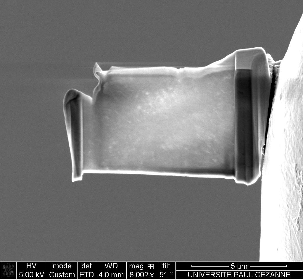
17 3 mm Recent FIB specimen holder


18 The royal road From the rock to the atomic image by TEM diamond saw the rock slice thin-section facility of a geological laboratory uncovered rock slate double face 1µm polish µm-thick Thermofusible resin (Lakeside, crystalbond) glass plate thin section a special thin section sugar piece 300 µm diamond wire saw polishing machines
 < 50 µm ready for the PIPS milling detach with a twizzer and wash the glue with")
19 Crossed nicols light microscopy to place the slots thin section -recognize the minerals from their optical properties -crystallographic orientation with 15 accuracy microdrilling around the slot and melt the glue underneath (< 200 C) < 50 µm ready for the PIPS milling detach with a twizzer and wash the glue with alcohol
 Ar+ ions, 5 -->2 kev, two guns 7-4 incidence. Polishing time 0.")
 Drawbacks -pollution by sputtering:")
20 The top for high-resolution electron microscopy (HRTEM) of most minerals Ion - milling systems Precision ion polishing system (PIPS) Ar+ ions, 5 -->2 kev, two guns 7-4 incidence. Polishing time 0.5h to 5 days for 50µm - thick thin section Advantages -large and thin surfaces to look at -wedge-shaped sample: extra-thin zones - gentle heating -high mechanical stability -reasonable damages (amorphisation) Drawbacks -pollution by sputtering: grid, specimen holder -needs to be trained for optimum use

21 1 mm Around the hole: hours of exploration to come + continuous C-coating --> essential for electron conduction to the TEM mass Ready to enter the microscope
22 Preparation of TEM specimens: The sampling problem: to be representative for larger scale to be meaningful "All thinned samples of the Earth crust for TEM enter a thimble while the crust volume is roughly km 3.So, good luck for sampling! David, Veblen, JHU, Baltimore
23 The direct lattice (blue) and the reciprocal lattice (green) A 2-D case
 nl 1/λ < 1-2 ----->only lattice planes // to the")

24 Diffraction by crystals Bragg's law 2d (hkl) sin = nl and for high-energy electrons: 2d (hkl) nl 1/λ < >only lattice planes // to the incident beam are diffracting very thin specimen ---> elongation of reciprocal lattice nodes --->relaxation of Bragg's conditions > many reflections at a time

 perfectly symetrical around the transmitted beam by centring the first - order Laue zone")
25 intersecting the 3D arrangement of the reciprocal lattice (RL) The SAED pattern = Visualisation of sub planar sections of the reciprocal lattice Tilting the sample in diffraction mode is exploring the RL in 3-D Double tilt, high-resolution, specimen holder ± 15 Procedure of alignment of a single crystal: find a crowdy SAED, put the zero-order Laue zone(zolz) perfectly symetrical around the transmitted beam by centring the first - order Laue zone (FOLZ) when visible! FOLZ ZOLZ


26 Microdiffraction patterns of some states of matter amorphous polycrystalline single crystal + disorder cylindrical lattice Quasi crystal seen along a 2-fold axis B. Devouard
27 The objective lens is the only one that matters In its focal plane, the diffraction pattern of the object In its image plane, the microscope performs a Fourier photosummation The Graal: the charge density projection of the crystal structure A biperiodic image = discrete sum (troncated) of sine variations of fringe contrast along diffraction vectors In the trigonometric form: (y,z)= k l F 0kl cos 2 (ky + lz + 0kl ) = F 000 Amplitude Wavelength Phase + F 010 cos 2 (y ) + F 020 cos 2 (2y+ 020 ) F 001 cos 2 (z+ 001 ) + F 002 cos 2 (2z+ 002 ) F 011 cos 2 (y+z+ 011 ) + F 022 cos 2 (2y+2z+ 022 ) +...

 roughly compensate for those phase offsets within the transfer window toward the")
28 Point-to-point resolutions at CINaM: 2.8 Å for 200 kv TEM 1.6Å or 2.1Å for 300kV TEM 0.5Å somewhere in the world Electronic image = recombination of discrete diffracted beams; not a «shadow» image that keep amplitudes and phases of diffracted waves but: dynamical diffraction + phase offsets due mainly to spherical aberration The Scherzer defocus (critical underfocusing) roughly compensate for those phase offsets within the transfer window toward the structure image d r = 0, 65l 3 / 4 Cs 1/ 4


29 Correct phases are essentiel to get a correct structure image Objective Aperture Back focal plane Diffraction vectors Wave shift


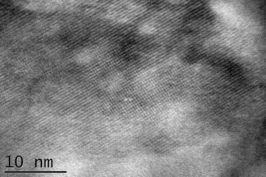
30 Very HR numerical scan of the image «nuclear» film circular selection FFT processing (FIJI application) l 02l 04l 06l 5 nm Recorded Diff pattern Quasi-atomic image of the biotite mica seen along <1 0 0> FFT now realistic substitute to the microdiffraction
(Transmission)+Electron+ Microscopy+for+Multi6Scale+ Porous+Materials+ + I6+Basic+principles+and+techniques!
+Electron+ Microscopy+for+Multi6Scale+ Porous+Materials+ + I6+Basic+principles+and+techniques!") (Transmission)+Electron+ Microscopy+for+Multi6Scale+ Porous+Materials+ + I6+Basic+principles+and+techniques! A.BARONNET,J.BERTHONNEAU&O.GRAUBY! Aix3MarseilleUniversité CentreInterdisciplinairedeNanosciencede
(Transmission)+Electron+ Microscopy+for+Multi6Scale+ Porous+Materials+ + I6+Basic+principles+and+techniques! A.BARONNET,J.BERTHONNEAU&O.GRAUBY! Aix3MarseilleUniversité CentreInterdisciplinairedeNanosciencede
STUDY & ANALYSIS OF ALUMINIUM FOIL AND ANATASE TITANIUM OXIDE (TiO2) USING TRANSMISSION ELECTRON MICROSCOPY
 USING TRANSMISSION ELECTRON MICROSCOPY") STUDY & ANALYSIS OF ALUMINIUM FOIL AND ANATASE TITANIUM OXIDE (TiO2) USING TRANSMISSION ELECTRON MICROSCOPY Ayush Garg Department of Chemical and Materials Engineering, University of Auckland, Auckland,
STUDY & ANALYSIS OF ALUMINIUM FOIL AND ANATASE TITANIUM OXIDE (TiO2) USING TRANSMISSION ELECTRON MICROSCOPY Ayush Garg Department of Chemical and Materials Engineering, University of Auckland, Auckland,
Microstructural Characterization of Materials
 Microstructural Characterization of Materials 2nd Edition DAVID BRANDON AND WAYNE D. KAPLAN Technion, Israel Institute of Technology, Israel John Wiley & Sons, Ltd Contents Preface to the Second Edition
Transmission Electron Microscopy (TEM) Prof.Dr.Figen KAYA
 Prof.Dr.Figen KAYA") Transmission Electron Microscopy (TEM) Prof.Dr.Figen KAYA Transmission Electron Microscope A transmission electron microscope, similar to a transmission light microscope, has the following components along
Transmission Electron Microscopy (TEM) Prof.Dr.Figen KAYA Transmission Electron Microscope A transmission electron microscope, similar to a transmission light microscope, has the following components along
Specimen Preparation Technique for a Microstructure Analysis Using the Focused Ion Beam Process
 Specimen Preparation Technique for a Microstructure Analysis Using the Focused Ion Beam Process by Kozue Yabusaki * and Hirokazu Sasaki * In recent years the FIB technique has been widely used for specimen
Electron Microscopy. Dynamical scattering
 Electron Microscopy 4. TEM Basics: interactions, basic modes, sample preparation, Diffraction: elastic scattering theory, reciprocal space, diffraction pattern, Laue zones Diffraction phenomena Image formation:
Signals from a thin sample
 Signals from a thin sample Auger electrons Backscattered electrons BSE Incident beam secondary electrons SE Characteristic X-rays visible light 1-100 nm absorbed electrons Specimen electron-hole pairs
TEM and Electron Diffraction Keith Leonard, PhD (1999) U. Cincinnati
 U. Cincinnati") TEM and Electron Diffraction Keith Leonard, PhD (1999) U. Cincinnati Electron Microscopes: Electron microscopes, such as the scanning electron microscope (SEM) and transmission electron microscope (TEM)
TEM and Electron Diffraction Keith Leonard, PhD (1999) U. Cincinnati Electron Microscopes: Electron microscopes, such as the scanning electron microscope (SEM) and transmission electron microscope (TEM)
Electron microscopy II
 Electron microscopy II Nanomaterials characterization I RNDr. Věra Vodičková, PhD. Interaction ction: electrons solid matter Signal types SE.secondary e - AE Auger s e - BSE back scattered e - X-ray photons,
The principles and practice of electron microscopy
 The principles and practice of electron microscopy Second Edition Ian M. Watt CAMBRIDGE UNIVERSITY PRESS Contents Preface tofirstedition page ix Preface to second edition xi 1 Microscopy with light and
CHEM-E5225 :Electron Microscopy Imaging II
 CHEM-E5225 :Electron Microscopy Imaging II D.B. Williams, C.B. Carter, Transmission Electron Microscopy: A Textbook for Materials Science, Springer Science & Business Media, 2009. Z. Luo, A Practical Guide
Diffraction Going further
 Diffraction Going further Duncan Alexander! EPFL-CIME 1 Contents Higher order Laue zones (HOLZ)! Kikuchi diffraction! Convergent beam electron diffraction (CBED)! HOLZ lines in CBED! Thickness measurements!
11.3 The analysis of electron diffraction patterns
 11.3 The analysis of electron diffraction patterns 277 diameter) Ewald reflecting sphere, the extension of the reciprocal lattice nodes and the slight buckling of the thin foil specimens all of which serve
METHOD FOR IMPROVING FIB PREPARED TEM SAMPLES BY VERY LOW ENERGY Ar + ION MILL POLISHING
 METHOD FOR IMPROVING FIB PREPARED TEM SAMPLES BY VERY LOW ENERGY Ar + ION MILL POLISHING Yaron Kauffmann, Tzipi Cohen-Hyams, Michael Kalina, Hila Sadan-Meltzman and Wayne D. Kaplan Dept. of Materials Engineering
Fundamentals of X-ray diffraction and scattering
 Fundamentals of X-ray diffraction and scattering Don Savage dsavage@wisc.edu 1231 Engineering Research Building (608) 263-0831 X-ray diffraction and X-ray scattering Involves the elastic scattering of
Single crystal X-ray diffraction. Zsolt Kovács
 Single crystal X-ray diffraction Zsolt Kovács based on the Hungarian version of the Laue lab description which was written by Levente Balogh, Jenő Gubicza and Lehel Zsoldos INTRODUCTION X-ray diffraction
Electron Probe Micro-Analysis (EPMA)
") Electron Probe Micro-Analysis (EPMA) Nilanjan Chatterjee, Ph.D. Principal Research Scientist 1 Electron Microprobe Facility Department of Earth, Atmospheric and Planetary Sciences Massachusetts Institute
Electron Probe Micro-Analysis (EPMA) Nilanjan Chatterjee, Ph.D. Principal Research Scientist 1 Electron Microprobe Facility Department of Earth, Atmospheric and Planetary Sciences Massachusetts Institute
EBSD Basics EBSD. Marco Cantoni 021/ Centre Interdisciplinaire de Microscopie Electronique CIME. Phosphor Screen. Pole piece.
 EBSD Marco Cantoni 021/693.48.16 Centre Interdisciplinaire de Microscopie Electronique CIME EBSD Basics Quantitative, general microstructural characterization in the SEM Orientation measurements, phase
CHAPTER 7 MICRO STRUCTURAL PROPERTIES OF CONCRETE WITH MANUFACTURED SAND
 99 CHAPTER 7 MICRO STRUCTURAL PROPERTIES OF CONCRETE WITH MANUFACTURED SAND 7.1 GENERAL Characterizing the mineralogy of the samples can be done in several ways. The SEM identifies the morphology of the
Imaging with Diffraction Contrast
 Imaging with Diffraction Contrast Duncan Alexander EPFL-CIME 1 Introduction When you study crystalline samples TEM image contrast is dominated by diffraction contrast. An objective aperture to select either
TEM imaging and diffraction examples
 TEM imaging and diffraction examples Duncan Alexander EPFL-CIME 1 Diffraction examples Kikuchi diffraction Epitaxial relationships Polycrystalline samples Amorphous materials Contents Convergent beam electron
Carnegie Mellon MRSEC
 Carnegie Mellon MRSEC Texture, Microstructure & Anisotropy, Fall 2009 A.D. Rollett, P. Kalu 1 ELECTRONS SEM-based TEM-based Koseel ECP EBSD SADP Kikuchi Different types of microtexture techniques for obtaining
LECTURE 7. Dr. Teresa D. Golden University of North Texas Department of Chemistry
 LECTURE 7 Dr. Teresa D. Golden University of North Texas Department of Chemistry Diffraction Methods Powder Method For powders, the crystal is reduced to a very fine powder or microscopic grains. The sample,
Transzmissziós és pásztázó elektronmikroszkópos minták készítése ionsugaras vékonyítással
 Transzmissziós és pásztázó elektronmikroszkópos minták készítése ionsugaras vékonyítással Radi Zsolt Technoorg Linda Kft., Budapest Oktatói és Doktorandusz Konferencia Visegrád, 2012 State-of-the-art materials
CHAPTER 4 SYNTHESIS, CHARACTERIZATION AND MICROENCAPSULATION PROCESS OF THE NANO SILICA
 70 CHAPTER 4 SYNTHESIS, CHARACTERIZATION AND MICROENCAPSULATION PROCESS OF THE NANO SILICA 4.1 INTRODUCTION This chapter is concerned with the synthesis of nano silica particles from the natural resources
Characterization of Materials Using X-Ray Diffraction Powder Diffraction
 Praktikum III, Fall Term 09 Experiment P1/P2; 23.10.2009 Characterization of Materials Using X-Ray Diffraction Powder Diffraction Authors: Michael Schwarzenberger (michschw@student.ethz.ch) Philippe Knüsel
Crystallographic Textures Measurement
 Crystallographic Textures Measurement D. V. Subramanya Sarma Department of Metallurgical and Materials Engineering Indian Institute of Technology Madras E-mail: vsarma@iitm.ac.in Macrotexture through pole
Atomic Structure of Ultrathin Gold Nanowires
 Supporting Information For Atomic Structure of Ultrathin Gold Nanowires Yi Yu, 1,2 Fan Cui, 1,2 Jianwei Sun, 1,2 and Peidong Yang* 1,2,3,4 1 Department of Chemistry, University of California, Berkeley,
TEM imaging and diffraction examples
 TEM imaging and diffraction examples Duncan Alexander EPFL-CIME 1 Diffraction examples Kikuchi diffraction Epitaxial relationships Polycrystalline samples Amorphous materials Contents Convergent beam electron
Observation in the GB (Gentle Beam) Capabilities
 Capabilities") A field-emission cathode in the electron gun of a scanning electron microscope provides narrower probing beams at low as well as high electron energy, resulting in both improved spatial resolution and
A field-emission cathode in the electron gun of a scanning electron microscope provides narrower probing beams at low as well as high electron energy, resulting in both improved spatial resolution and
UNIVERSITY OF OSLO. Faculty of Mathematics and Natural Sciences
 Page 1 UNIVERSITY OF OSLO Faculty of Mathematics and Natural Sciences Exam in MENA3100 Characterization of materials Day of exam: 12th. June 2015 Exam hours: 14:30 This examination paper consists of 5
Why does the growth rate slow down as a precipitate thickens during diffusion-controlled growth?
 Part II: Worked Examples H. K. D. H. Bhadeshia Question 14 Why does the growth rate slow down as a precipitate thickens during diffusion-controlled growth? The surface of a metal can be nitrided to form
NEMI Sn Whisker Modeling Group Part 2:Future Work
 NEMI Sn Whisker Modeling Group Part 2:Future Work IPC/NEMI Meeting Maureen Williams, NIST Irina Boguslavsky, NEMI Consultant November 7, 2002 New Orleans, LA Capabilities of NEMI Modeling Group NEMI Fundamental
Transmission Kikuchi Diffraction in the Scanning Electron Microscope
 Transmission Kikuchi Diffraction in the Scanning Electron Microscope Robert Keller, Roy Geiss, Katherine Rice National Institute of Standards and Technology Nanoscale Reliability Group Boulder, Colorado
Lesson 1 X-rays & Diffraction
 Lesson 1 X-rays & Diffraction Nicola Döbelin RMS Foundation, Bettlach, Switzerland February 11 14, 2013, Riga, Latvia Electromagnetic Spectrum X rays: Wavelength λ: 0.01 10 nm Energy: 100 ev 100 kev Interatomic
FePd (216 Å) grown on (001) MgO. 2θ(deg)
 grown on (001) MgO. 2θ(deg)") Major Findings 1. FePd thin films The structural characterization of the films grown at various substrate temperatures (RT- 700 o C) was performed ex-situ using X-Ray Diffraction (XRD). The optimum substrate
Major Findings 1. FePd thin films The structural characterization of the films grown at various substrate temperatures (RT- 700 o C) was performed ex-situ using X-Ray Diffraction (XRD). The optimum substrate
This lecture is part of the Basic XRD Course.
 This lecture is part of the Basic XRD Course. Basic XRD Course 1 A perfect polycrystalline sample should contain a large number of crystallites. Ideally, we should always be able to find a set of crystallites
JSM-7800F Field Emission Scanning Electron Microscope
 JSM-7800F catalogue JSM-7800F Field Emission Scanning Electron Microscope We provide high performance The Ultimate Research Tool for Multi-Disciplinary Research Institutions Extreme resolution The super
Kinematical theory of contrast
 Kinematical theory of contrast Image interpretation in the EM the known distribution of the direct and/or diffracted beam on the lower surface of the crystal The image on the screen of an EM = the enlarged
Specimen configuration
 APPLICATIONNOTE Model 1040 NanoMill TEM specimen preparation system Specimen configuration Preparing focused ion beam (FIB) milled specimens for submission to Fischione Instruments. The Model 1040 NanoMill
John de Laeter Centre
 John de Laeter Centre Major research infrastructure hub at Curtin University, Perth, W.A. ~$30M worth of microscopes, spectrometers, diffractometers and experimental facilities AuScope partner, Microscopy
The object of this experiment is to test the de Broglie relationship for matter waves,
 Experiment #58 Electron Diffraction References Most first year texts discuss optical diffraction from gratings, Bragg s law for x-rays and electrons and the de Broglie relation. There are many appropriate
Chapter 3 Basic Crystallography and Electron Diffraction from Crystals. Lecture 9. Chapter 3 CHEM Fall, L. Ma
 Chapter 3 Basic Crystallography and Electron Diffraction from Crystals Lecture 9 Outline The geometry of electron diffraction Crystallography Kinetic Theory of Electron diffraction Diffraction from crystals
Silver Diffusion Bonding and Layer Transfer of Lithium Niobate to Silicon
 Chapter 5 Silver Diffusion Bonding and Layer Transfer of Lithium Niobate to Silicon 5.1 Introduction In this chapter, we discuss a method of metallic bonding between two deposited silver layers. A diffusion
Advanced Manufacturing Choices
 Advanced Manufacturing Choices Table of Content Mechanical Removing Techniques Ultrasonic Machining (USM) Sputtering and Focused Ion Beam Milling (FIB) Ultrasonic Machining In ultrasonic machining (USM),
INSTRUMENTAL TECHNIQUES FOR PARTICLE SIZE DETERMINATION
 CHAPTER V INSTRUMENTAL TECHNIQUES FOR PARTICLE SIZE DETERMINATION 5.1 INTRODUCTION Particle size determination is very essential and important while working with nanomaterials. There are a few good experimental
EMSE Weak-Beam Dark-Field Technique
 Weak-Beam Dark-Field Technique 1 Weak-Beam Dark-Field Imaging Basic Idea recall bright-field contrast of dislocations: specimen close to Bragg condition, s î 0 near the dislocation core, some planes curved
EBSD Electron BackScatter Diffraction Principle and Applications
 EBSD Electron BackScatter Diffraction Principle and Applications Dr. Emmanuelle Boehm-Courjault EPFL STI IMX Laboratoire de Simulation des Matériaux LSMX emmanuelle.boehm@epfl.ch 1 Outline! Introduction!
SUPPLEMENTARY INFORMATION
 High Electrochemical Activity of the Oxide Phase in Model Ceria- and Ceria-Ni Composite Anodes William C. Chueh 1,, Yong Hao, WooChul Jung, Sossina M. Haile Materials Science, California Institute of Technology,
Earth & Planetary Science Applications of X-Ray Diffraction: Advances Available for Research with our New Systems
 Earth & Planetary Science Applications of X-Ray Diffraction: Advances Available for Research with our New Systems James R. Connolly Dept. of Earth & Planetary Sciences University of New Mexico 401/501
Introduction to Electron Microscopy Andres Kaech
 Center for Microscopy and Image Analysis Introduction to Electron Microscopy Andres Kaech The types of electron microscopes Transmission electron microscope (TEM) Scanning electron microscope (SEM) 1 The
Scanning Electron Microscope & Surface Analysis. Wageningen EM Centre Marcel Giesbers
 Scanning Electron Microscope & Surface Analysis Wageningen EM Centre Marcel Giesbers Scanning Electron Microscope & Surface Analysis SEM vs Light Microscope and Transmission EM Secondary Electron Imaging
Transmission Electron Microscopy. J.G. Wen, C.H. Lei, M. Marshall W. Swiech, J. Mabon, I. Petrov
 Advanced Materials Characterization Workshop Transmission Electron Microscopy J.G. Wen, C.H. Lei, M. Marshall W. Swiech, J. Mabon, I. Petrov Supported by the U.S. Department of Energy under grants DEFG02-07-ER46453
Atomic Densities. Linear Density Number of atoms per length whose centers lie on the direction vector for a specific crystallographic direction.
 Atomic Densities Linear Density Number of atoms per length whose centers lie on the direction vector for a specific crystallographic direction. Planar Density Number of atoms per unit area that are centered
In Situ Observation of Dislocation Nucleation and Escape in a Submicron Al Single Crystal
 Supplementary Information for In Situ Observation of Dislocation Nucleation and Escape in a Submicron Al Single Crystal Sang Ho Oh*, Marc Legros, Daniel Kiener and Gerhard Dehm *To whom correspondence
Growth of monocrystalline In 2 O 3 nanowires by seed orientation dependent vapour-solid-solid mechanism
 Electronic Supplementary Material (ESI) for Journal of Materials Chemistry C. This journal is The Royal Society of Chemistry 2014 Electronic Supplementary Information (ESI) Growth of monocrystalline In
INGE Engineering Materials. Chapter 3 (cont.)
") Some techniques used: Chapter 3 (cont.) This section will address the question how do we determine the crystal structure of a solid sample? Electron microscopy (by direct and indirect observations) Scanning
Some techniques used: Chapter 3 (cont.) This section will address the question how do we determine the crystal structure of a solid sample? Electron microscopy (by direct and indirect observations) Scanning
Identification of Crystal Structure and Lattice Parameter. for Metal Powders Using X-ray Diffraction. Eman Mousa Alhajji
 Identification of Crystal Structure and Lattice Parameter for Metal Powders Using X-ray Diffraction Eman Mousa Alhajji North Carolina State University Department of Materials Science and Engineering MSE
Practical 2P8 Transmission Electron Microscopy
 Practical 2P8 Transmission Electron Microscopy Originators: Dr. N.P. Young and Prof. J. M. Titchmarsh What you should learn from this practical Science This practical ties-in with the lecture course on
Practical 2P8 Transmission Electron Microscopy
 Practical 2P8 Transmission Electron Microscopy Originators: Dr. M. L. Jenkins and Prof. J. M. Titchmarsh What you should learn from this practical Science This practical ties-in with the lecture course
SECTION A. NATURAL SCIENCES TRIPOS Part IA. Friday 4 June to 4.30 MATERIALS AND MINERAL SCIENCES
 NATURAL SCIENCES TRIPOS Part IA Friday 4 June 1999 1.30 to 4.30 MATERIALS AND MINERAL SCIENCES Answer five questions; two from each of sections A and B and one from section C. Begin each answer at the
CHAPTER 4. SYNTHESIS OF ALUMINIUM SELENIDE (Al 2 Se 3 ) NANO PARTICLES, DEPOSITION AND CHARACTERIZATION
 NANO PARTICLES, DEPOSITION AND CHARACTERIZATION") 40 CHAPTER 4 SYNTHESIS OF ALUMINIUM SELENIDE (Al 2 Se 3 ) NANO PARTICLES, DEPOSITION AND CHARACTERIZATION 4.1 INTRODUCTION Aluminium selenide is the chemical compound Al 2 Se 3 and has been used as a precursor
40 CHAPTER 4 SYNTHESIS OF ALUMINIUM SELENIDE (Al 2 Se 3 ) NANO PARTICLES, DEPOSITION AND CHARACTERIZATION 4.1 INTRODUCTION Aluminium selenide is the chemical compound Al 2 Se 3 and has been used as a precursor
The Significance of Bragg s Law in Electron Diffraction and Microscopy and Bragg s Second Law
 The Significance of Bragg s Law in Electron Diffraction and Microscopy and Bragg s Second Law Colin Humphreys University of Cambridge Bragg Symposium Adelaide 6 December 2012 Bragg s Second Law E. W.
Strain. Two types of stresses: Usually:
 Stress and Texture Strain Two types of stresses: microstresses vary from one grain to another on a microscopic scale. macrostresses stress is uniform over large distances. Usually: macrostrain is uniform
JEOL JXA-8200 Superprobe
 JEOL JXA-8200 Superprobe Electron gun Liq N 2 for EDS Electron gun Condenser lens Optical Microscope Optical Microscope EDS WDS SE Liq N 2 EDS BSE Objective lens WDS Sample exchange chamber Stage High
Chapter 3 Silicon Device Fabrication Technology
 Chapter 3 Silicon Device Fabrication Technology Over 10 15 transistors (or 100,000 for every person in the world) are manufactured every year. VLSI (Very Large Scale Integration) ULSI (Ultra Large Scale
Development of New Generation Of Coatings with Strength-Ductility Relationship, Wear, Corrosion and Hydrogen Embrittlement Resistance Beyond the
 Development of New Generation Of Coatings with Strength-Ductility Relationship, Wear, Corrosion and Hydrogen Embrittlement Resistance Beyond the Current Materials Accomplishments till date As the structural
INTEGRATED OPTICAL ISOLATOR
 INTEGRATED OPTICAL ISOLATOR Presented by Gokhan Ozgur Advisor: Dr. Gary Evans July 02, 2004 Electrical Engineering - SMU INTRODUCTION They are used to eliminate light that is back-reflected, from splices
High-resolution phase contrast imaging, aberration corrections, and the specifics of nanocrystals
 High-resolution phase contrast imaging, aberration corrections, and the specifics of nanocrystals Pages 450-459, in Methods and applications in crystallographic computing, S.R. Hall and T. Ashida, Proc.
Oxidation behavior of Cu nanoclusters in hybrid thin films
 Oxidation behavior of Cu nanoclusters in hybrid thin films Harm Wulff,* Steffen Drache*, Vitezslav Stranak**, Angela Kruth*** *EMAU Greifswald, **South Bohemian University, Budweis, *** INP Greifswald
Chapter 3: Powders Production and Characterization
 Chapter 3: Powders Production and Characterization Course Objective... To introduce selective powder production processes and characterization methods. This course will help you : To understand properties
Transmission Kikuchi Diffraction in the Scanning Electron Microscope
 in the Scanning Electron Microscope Robert Keller, NIST, Boulder, USA Daniel Goran, Bruker Nano, Berlin, Germany 24 th April 2013 Innovation with Integrity in the Scanning Electron Microscope Robert Keller,
Polycrystalline and microcrystalline silicon
 6 Polycrystalline and microcrystalline silicon In this chapter, the material properties of hot-wire deposited microcrystalline silicon are presented. Compared to polycrystalline silicon, microcrystalline
Growth Of TiO 2 Films By RF Magnetron Sputtering Studies On The Structural And Optical Properties
 Journal of Multidisciplinary Engineering Science and Technology (JMEST) Growth Of TiO 2 Films By RF Magnetron Sputtering Studies On The Structural And Optical Properties Ahmed K. Abbas 1, Mohammed K. Khalaf
High Resolution X-ray Diffraction
 High Resolution X-ray Diffraction Nina Heinig with data from Dr. Zhihao Donovan Chen, Panalytical and slides from Colorado State University Outline Watlab s new tool: Panalytical MRD system Techniques:
MODEL 1051 TEM Mill ION MILLING. Ion milling is used on physical science. specimens to reduce thickness to electron
 MODEL 1051 TEM Mill A state-of-the-art ion milling and polishing system offering reliable, high performance specimen preparation. It is compact, precise, and consistently produces high-quality transmission
Grain Sizes and Surface Roughness in Platinum and Gold Thin Films. L.L. Melo, A. R. Vaz, M.C. Salvadori, M. Cattani
 Journal of Metastable and Nanocrystalline Materials Vols. 20-21 (2004) pp. 623-628 online at http://www.scientific.net 2004 Trans Tech Publications, Switzerland Grain Sizes and Surface Roughness in Platinum
IBS/e Ion Beam Sputter Deposition and Etching System. IBS/e with KDC-10 Ion Beam Sputter Deposition and Etching System with Kaufman Ion Source
 IBS/e Ion Beam Sputter Deposition and Etching System IBS/e with KDC-10 Ion Beam Sputter Deposition and Etching System with Kaufman Ion Source The Model IBS/e is a high vacuum thin film deposition system
MODEL PicoMill TEM specimen preparation system. Achieve ultimate specimen quality free from amorphous and implanted layers
 MODEL 1080 PicoMill TEM specimen preparation system Combines an ultra-low energy, inert gas ion source, and a scanning electron column with multiple detectors to yield optimal TEM specimens. POST-FIB PROCESSING
Supplementary Figure S1 Crystal structure of the conducting filaments in sputtered SiO 2
 Supplementary Figure S1 Crystal structure of the conducting filaments in sputtered SiO 2 based devices. (a) TEM image of the conducting filament in a SiO 2 based memory device used for SAED analysis. (b)
Dislocations Linear Defects
 Dislocations Linear Defects Dislocations are abrupt changes in the regular ordering of atoms, along a line (dislocation line) in the solid. They occur in high density and are very important in mechanical
Introduction to Powder Diffraction/Practical Data Collection
 Durham University Chemistry Department Introduction to Powder Diffraction/Practical Data Collection Dr Ivana Evans Durham, January 2007 Durham Outline Information in a powder pattern What is diffraction
Directional Amorphization of Boron Carbide Subjected to Laser Shock Compression
 Supporting Information Directional Amorphization of Boron Carbide Subjected to Laser Shock Compression This PDF file contains: Figures S1 to S4 Supplementary Text : 1. Materials and initial characterization
Supporting Information
 Supporting Information Dynamics and Removal Pathway of Edge Dislocations in Imperfectly Attached PbTe Nanocrystal Pairs; Towards Design Rules for Oriented Attachment Justin C. Ondry,, Matthew R. Hauwiller,,
Focused Ion Beam CENTRE INTERDISCIPLINAIRE DE MICROSCOPIE ELECTRONIQUE. Marco Cantoni, EPFL-CIME CIME ASSEMBLEE GENERALE 2007
 Focused Ion Beam @ CENTRE INTERDISCIPLINAIRE DE MICROSCOPIE ELECTRONIQUE Present situation and vision Marco Cantoni, EPFL-CIME Dual Beam Nova 600 Nanolab from FEI Company FE-SEM & FIB: Ga LMIS 4 Gas Injector
Electron Microscopy Sciences
 Electron Microscopy Sciences INSTRUCTIONAL MANUAL CAT. 80058-ST X-Checker Standard CAT. 80058-BN X-Checker Boron Nitride CAT. 80058-EX X-Checker Extra P.O. Box 550 s1560 Industry Road s Hatfield PA 19440
The application of scanning electron beam anomalous transmission patterns in mineralogy
 MINERALOGICAL MAGAZINE, JUNE 1969, VOL. 37, NO. 286 The application of scanning electron beam anomalous transmission patterns in mineralogy M. P. JONES, B.SC., D.I.C., A.M.I.M.M., AND J. GAVRILOVIC, PH.D.,
X-RAY DIFFRACTION IN SEMICONDUCTOR INDUSTRY AND RESEARCH
 X-RAY DIFFRACTION IN SEMICONDUCTOR INDUSTRY AND RESEARCH M. Leszczyński High Pressure Research Center UNIPRESS, Sokolowska 29/37, 01 142 Warsaw, Poland, e-mail: mike@unipress.waw.pl ABSTRACT The paper
9/28/2013 9:26 PM. Chapter 3. The structure of crystalline solids. Dr. Mohammad Abuhaiba, PE
 Chapter 3 The structure of crystalline solids 1 2 Why study the structure of crystalline solids? Properties of some materials are directly related to their crystal structure. Significant property differences
MODEL NanoMill TEM Specimen Preparation System. Ultra-low-energy, inert-gas ion source. Concentrated ion beam with scanning capabilities
 MODEL 1040 NanoMill TEM Specimen Preparation System The NanoMill system uses an ultra-low energy, concentrated ion beam to produce the highest quality specimens for transmission electron microscopy. Ultra-low-energy,
Grain Contrast Imaging in UHV SLEEM
 Materials Transactions, Vol. 51, No. 2 (2010) pp. 292 to 296 Special Issue on Development and Fabrication of Advanced Materials Assisted by Nanotechnology and Microanalysis #2010 The Japan Institute of
Texture Analysis in MSE
 Texture Analysis in MSE 집합조직제어연구실 서울대학교재료공학부 Texture (Preferred Orientation) Similarity of Texture E.T?! 한쪽을쳐다보고있는사람들여러방향을쳐다보는 Randomly Preferred Oriented What a Wonderful & Beautiful Life! Scientific
Lesson 1 Good Diffraction Data
 Lesson 1 Good Diffraction Data Nicola Döbelin RMS Foundation, Bettlach, Switzerland Digital Diffractometers Transmission Geometry Debye-Scherrer Geometry Reflective Geometry Bragg-Brentano Geometry Glass
Advanced Methods for Materials Research. Materials Structure Investigations Materials Properties Investigations
 Advanced Methods for Materials Research Materials Structure Investigations Materials Properties Investigations Advanced Methods for Materials Research 1. The structure and property of sample and methods
Thin Film Characterizations Using XRD The Cases of VO2 and NbTiN
 Thin Film Characterizations Using XRD The Cases of VO2 and NbTiN A thesis submitted in partial fulfillment of the requirement for the degree of Bachelor of Arts / Science in Physics from The College of
CRYSTAL STRUCTURE DETERMINATION OF PHARMACEUTICALS WITH ELECTRON DIFFRACTION
 CRYSTAL STRUCTURE DETERMINATION OF PHARMACEUTICALS WITH ELECTRON DIFFRACTION Dr. Partha Pratim Das Application Specialist, NanoMEGAS SPRL, Belgium pharma@nanomegas.com www.nanomegas.com This document was
X-RAY DIFFRACTIO N B. E. WARREN
 X-RAY DIFFRACTIO N B. E. WARREN Chapter 1 X-Ray Scattering by Atom s 1.1 Classical scattering by a free electron 1 1.2 Polarization by scattering 4 1.3 Scattering from several centers, complex representation
Monday: Y42 G53 Tuesday: Y42 G53 Wednesday: Y42 J11
 Locations: Irchel building 42, Level H and F Locations: Irchel building 42, Level H and F Self-study sessions: Monday: Y42 G53 Tuesday: Y42 G53 Wednesday: Y42 J11 1 Center for Microscopy and Image Analysis
 LA-UR-01-3685 Approved for public release; distribution is unlimited. Title: USING A MULTI-DISCIPLINARY APPROACH, THE FIRST ELECTRON BACKSCATTERED KIKUCHI PATTERNS WERE CAPTURED FOR A PLUTONIUM ALLOY Author(s):
SUPPLEMENTARY INFORMATIONS
 SUPPLEMENTARY INFORMATIONS Dynamic Evolution of Conducting Nanofilament in Resistive Switching Memories Jui-Yuan Chen, Cheng-Lun Hsin,,, Chun-Wei Huang, Chung-Hua Chiu, Yu-Ting Huang, Su-Jien Lin, Wen-Wei