Advances in Printed Electronic Materials that Meet Cost and Performance Needs
|
|
|
- Conrad Harper
- 6 years ago
- Views:
Transcription

1 Advances in Printed Electronic Materials that Meet Cost and Performance Needs Mark S. Critzer DuPont Microcircuit Materials Research Triangle Park, NC mcm.dupont.com
2 Agenda DuPont & Printed Electronics Applications & Materials Enable Lower Cost Trends & Challenges New, Differentiated Material & Process Solutions Summary


3 DuPont 2012 Segment Sales $3.4B Nutrition & Health $10.4B Agriculture $1.2B Industrial Biosciences $2.7B Electronics & Communications $34.8B* $6.4B Performance Materials $7.2B Performance Chemicals $3.8B Safety & Protection * Total company sales exclude transfers.


4 Microcircuit Materials Business Over 40 Years

 Conductors:")


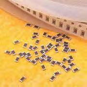
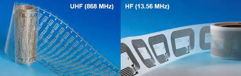
5 Traditional Printed Electronics at DuPont Materials (>95% Screen Print) Conductors: Silver, Gold, Copper, Alloys Dielectrics Multilayer, Cross-over, Encapsulant Resistors Carbon, Ruthenium Applications / Substrates Membrane Switch, EL / PET Film Rear Window Defogger / Glass Hybrid Microelectronics / Alumina Thick Film Multilayer Hybrid Battery Tester Chip Resistors Specialty PTC, Phosphor, ITO Photovoltaic / Silicon Thin Film PV / Foil Bio Test Strip Hybrid IC on Alumina RFID Antenna EL Lamps/Backlight Membrane Touch Switch Photovoltaic Si Cells


6 MCM - Printed Electronics Current Products & Applications Flexible TF Photovoltaics Ag grid and bus bar Biomedical sensors Au, Ag/AgCl, carbon electrodes Interconnects and membrane switches Ag, C, dielectric Electroluminescent lamps Ag, phosphor, dielectric, carbon RFID Ag antenna Displays, OLEDs, touch screens Ag and C grid lines and connectors R&D Ink-jet inks Nano-Ag powders and inks Transparent conductors Core Competencies Fine powder production Polymer chemistry Dispersion techniques Imaging techniques Rheology Coating and Casting Deposition Flat Screen Rotary screen Flexography Dip Spray


7 Printed Electronics application examples Displays Courtesy of Ascent Flex TF PV Touch Screens OLEDS Courtesy of Holst Centre Courtesy of Holst Centre Smart Packaging Courtesy of Power Paper Printed Batteries Flexible Displays Courtesy of Storaenso
8 Current Focus Area Technology Leadership & New Product/Application Development with Superior Functionality and Lower Total Cost to Customers


9 Screen Printed, Self Limiting Heaters Enabling Ink Materials North American Rescue Hypothermia Prevention Vests Polyester or Polyimide substrate NEW, Robust PTC Carbon Inks! Heats, but is Self Limiting (fails cold) New Formulations Replace 7282 Improved Temperature Stability No Pre-Conditioning Improved Compatibility w/adhesives NEW, High Conductivity Silver Inks! Low Enough R for Single Print Excellent Crease Resistance/Flexibility Seat Heater WET Automotive Silver Print PTC Carbon Print Finished Heater PTC Self Limiting Auto Seat Heaters Address Liability Concerns Eliminate Controller and Temperature sensors, providing ~35% savings* vs. Incumbent Heated Wire Technology Lowest Energy Consumption technology * Estimate


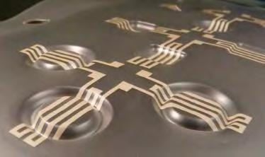
10 Silver Conductors for 3D Thermoforming In-Mold Electronics Side View 2.5 in thick to accommodate wire and 16 connectors Standard Ag Ink Reference New, Stretchable/Flexible Ag Ink! Side View No wires. Just one connector Enabling Ink Materials NEW, Ultra Flexible Silver Conductors STRETCH >75% Can withstand high temperature thermoform and In-Mold processing Maintains Electrical Performance NEW, Barrier & Insulating Dielectrics Can withstand high temperature, thermoform and In-Mold processing UV & Thermal Processing Automotive, Appliance, Medical, etc. Capacitive Touch Design replaces Mechanical Switches for Simplicity, Reliability, Aesthetics Space & Weight Reduction, plus easier to assemble Courtesy of T-Ink


11 Thermoforming / In-Mold Electronics Trends & Applications Eliminate electro-mechanical switches / knobs / etc. Reduced cost Reduced tooling and assembly costs Simpler supply chain Smaller, thinner, lighter More reliable Unlimited design options Drag and Drop design Quick turn prototyping Prototyping Capability at DuPont 4 th Qtr 2013 Design Capabilities 20 x 20 x4 Printing & Thermoforming capability Multi-color UV, Thermoset, Hard-Coat Processing Injection Molding via DuPont Performance Polymers Polycarbonate, Polyolefin substrates & Others Courtesy of Formech Inc.
12 Trends in Materials Cost & Performance

13 Trend # 1 Impact of Precious Metals Price Unpredictable, especially Silver since 2005 Silver < $10/T.O with relatively low volatility; Silver Peaked at $49/T.O. in 2011; Silver is around $20/T.O. today but what about 2014? 2016? How can users protect themselves against future cost spikes?
14 Solution # 1 Introduce New, Lower Cost Conductors It isn t always that simple, however. What is the Cost Target? >20% Reduction in Price ($/gr), and/or more Price Stability vs Ag cost? Other considerations such as Coverage (cm2/g); Screen Life? Additional capital equipment required for processing? What is Acceptable Electrical Performance? Resistivity (mω/ /mil)--how efficiently does the ink utilize % Ag? Resistance (mω/ )--How thick do you have to print to get Low Ohms? Physical Performance? Adhesion, Crease Resistance, Line & Space Resolution Substrates other than PET film? (Coated Papers, Woven, Polyolefins) Long Term Aging Stability; Migration Resistance
15 New! (July 2013) Lower Cost Thermal Cure Ag/Composite Conductors Targeted Resistivity Ranges Allows designers to use inks with lower cost, based on track dimensions Each application has different conductivity requirements PE850, PE825 commercially available now Reduced-cost, higher resistivity versions under development Resistivity decade targets between 5 50 milliohms/sq/mil Drop-In Replacement in Most Cases No additional equipment required Use current printing/drying process Designed to meet ASTM specifications for generic MTS and Printed Electronics applications Conventional Solution for the Conventional Approach 9/4/2013
, Clemson (Sonoco), & Cal Poly State Long History of DuPont Collaboration with University Programs in Electronics GOAL:")
16 Trend # 2 Convergence of Two Industries Graphics Printing Visual Performance Roll-2-Roll Assets High Speed, Low Cost Printing Electronics Functional Performance Precision Patterning Clean Rooms Universities are Playing a Key Role Currently with Western Michigan (CAPE), Clemson (Sonoco), & Cal Poly State Long History of DuPont Collaboration with University Programs in Electronics GOAL: Higher Speed, Lower Cost electronics
17 Solution #2 Develop Faster Curing Techniques High Volume R2R Printing Requires Fast Drying Highly Conductive Materials = Thicker Prints (solvent removal critical) Commercial Polymer Thick Film Inks have limitations Traditional drying equipment generally not sufficient Belt Oven: 120C for 2-6 minutes; Reel2Reel: 140C for 1 minute Slow ramp-up of heat to substrate; limited airflow & turnover Area of printed ink per impression too large Other Issues for High Speed Printing Include: Limited # of Commercial Electronic Inks Sample size too small to make cost-effective prototypes
18 9/4/2013 Curing Techniques for Printed Electronics Thermal Traditional process--may require high temps for extended times UV Limited Mostly to Dielectrics; Inefficient for opaque conductors Photonic Pulsed light, rapid sintering of particles, rapid solvent evaporation Other Laser Selective exposure by scanning with focused laser Microwave Rapid sintering, low penetration depths (~ 1.5 µ) Electrical Apply voltage across a printed structure, rapid sintering possible Plasma Sintering by exposure to low pressure plasma, e.g. argon Chemical Room temp process, chemically induced coalescence


19 Photonic Curing/ Pulsed Sintering High intensity strobe sinters metal containing inks on a variety of conventional and low cost substrates Sintering times are in the millisecond range High temperatures achieved locally for short periods of time Convenient: noncontact process, ambient conditions SINTERON 2000 Process variables are adjusted to accommodate ink and application (strobe energy, pulse length, # of pulses, web speed) New Focus on Photonic Curing of Base Metal Inks for High Speed Printing Applications PULSEFORGE 3300 Commercial Units: NovaCentrix PulseForge Xenon SINTERON Holst Center / Philips Aachen 9/4/2013


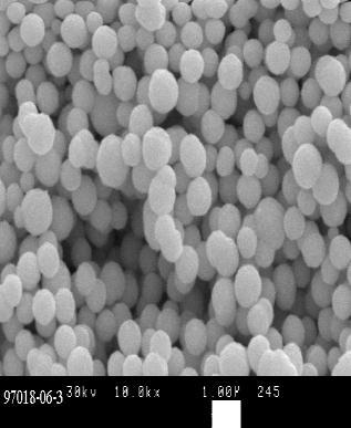
20 Low Cost Conductors Before / After Photonic Curing Ag Flake Thermal Cure 140C / 10min Photonic Cure Ag Sphere
21 Photonic Curing Behavior for PE815 Photonic Cure Profile for PE815 95% CI for the Mean Resistivity (mω/ /mil) mω/ /mil 9.7 J/cm mω/ /mil 10.3 J/cm mω/ /mil 10.1 J/cm 2 Voltage (V) Pulse Length (µsec) Voltage (V) /4/2013 Minimum Resistivity achieved with several pulse voltage / pulse length combinations Total exposure dose for each resistivity minimum is similar
22 Lower Cost Conductors w/ Photonic Curing Resistivity (mohms/sq/mil) Product ID Material Oven (140C, 10 min) Photonic Curing(*) 5064H 5025 PE PE815 PE Silvers Carbons 28,400 16,200 Alloys & Composites PE815 Designed for Photonic Curing / Lamination/ Hot Roll Calendering PE850, PE825 Designed for Thermal Cure only PE815, PE825, PE850 Available Now Controlled Lab Testing with NovaCentrix PulseForge 3200 Printed/dried on DuPont Teijin Films Melinex ST ,000 16, The data above reflects results under a given experimental design and under controlled conditions, and should not be used to establish specification limits or used alone as the basis of design or appropriateness for use in a particular process or product configuration. The data provided herein shall not constitute a warranty of any kind.


23 Improved Performance Using Lamination / Hot Roll Calendering Smart Card Production Unit Courtesy Muhlbauer Trends & Applications Contactless Smart Cards in Production since early 1990 s Calendering used in paper & film manufacturing Desire to switch from high Ag-content to new Alloys Additive High-Speed Screen Printing vs Etched Foil In use with DuPont 5029 Ag; PE815 & New Alloy Inks* New, targeted resistivity inks under development Smart Card, RFID, MTS, Biomedical, Smart Packaging Uniaxial Lamination or Continuous Hot Roll Calendering* *Patents Pending Prototyping Capability at DuPont Small scale Sheet or Roll Calendering up to 130C 18 x18 Uniaxial Lamination up to 130C New Printed Electronics RTP 4 th Qtr 2013 Lab-Scale Calendering Unit Courtesy Mathis AG
24 Lamination / Calendered Surface Dried Print Laminated / Hot Roll Calendered
 Lower Ag content Low Resistivity High Coverage Relative Cost 80 70 60 5064H PE85X PE82X 5524 PE825 (Composite) Lowest Cost Good Resistivity Lower $/TO Sensitivity 50 PE85X")
25 Conductor Costs Thermal (140C) Cure Protection against rising Silver Costs Relative Conductor Cost with $30/T.O. and $50/T.O 5064H PE850 (Silver) Lower Ag content Low Resistivity High Coverage Relative Cost H PE85X PE82X 5524 PE825 (Composite) Lowest Cost Good Resistivity Lower $/TO Sensitivity 50 PE85X PE82X Resistivity (mohms/sq./25um) 40
26 Conductor Costs Photonic Cure / Lamination / Calendering Protection against rising Silver Costs Relative Conductor Cost with $30/T.O. and $50/T.O. 5064H PE815 (Alloy) Lowest Cost Good Resistivity Lower $/TO Sensitivity 80 PE85X 5524 Relative Cost H PE85X PE81X PE81X Resistivity (mohms/sq./25um) 40


27 Printed Electronics on Paper Trends & Applications RFID Labels for Inventory/Supply Chain Passports/IDs/Document Security I/C Connect to USB/Readers (IntelliPaper) Solvent or Water Based Flexo/Screen Print Electrical Performance vs Non-Permeable Number of New Substrate Technologies


28 Printed Solar Cells on Paper 250 PV Cells = 50 Volts PV Cells Screen Printed on Newspaper Trends & Applications Low Cost PV need Low Cost Substrate & Inks Thin Film Electrode PEDOT vs High-Cost ITO High Speed Reel-2-Reel Printing for Volume Flexibility = Better Efficiency/Crease Performance Laminated w/ Plastic Film for Moisture Resistance


29 Emerging Printed Electronics Printed Electronic Packaging Packaging Diversification Logistics Traceability Sensing Medical Advertising Diversification Interactivity Visual Impact
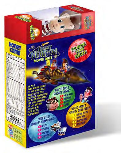
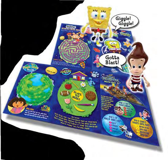

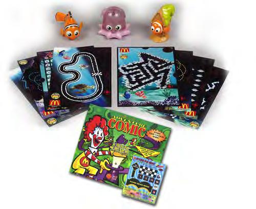

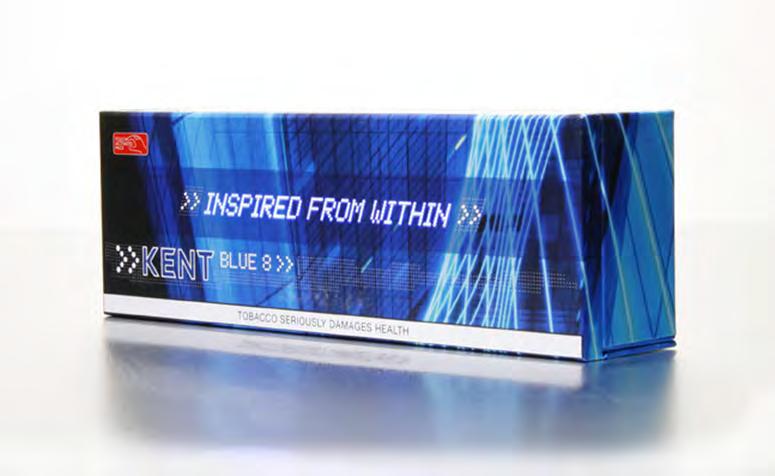
30 Printed Electronics on Paper Courtesy T-Ink Hallmark Interactive McDonald s Toy Kent Touch/LED Package Interactive Cereal Box
31 Summary New Printed Functional Inks can Enable Lower Cost Solutions Enabled by advances in design, processing, and materials In-Mold Electronics & lower cost help drive innovation Alternative substrates to traditional PET film (Paper, etc.) Screen Printing is still the dominant printing technique Introduction of NEW Lower Cost Conductor Technology For traditional thermal curing & emerging photonic curing Can be used with lamination & hot roll calendering Provides protection against precious metal pricing More new formulations & unique applications going forward There are many Commercial / Developmental Material Options Application / Design Dependent Work with the Ink Materials Suppliers
32 9/4/2013 Thank you
Polymer Thick Film Paste & Material Compatibility Discussion
 Polymer Thick Film Paste & Material Compatibility Discussion John Crumpton September 14, 2015 Agenda What is a Polymer thick Film Basic Thick Film Paste Technology Standard Processing (Printing & Drying)
LOW TEMPERATURE PHOTONIC SINTERING FOR PRINTED ELECTRONICS. Dr. Saad Ahmed XENON Corporation November 19, 2015
 LOW TEMPERATURE PHOTONIC SINTERING FOR PRINTED ELECTRONICS Dr. Saad Ahmed XENON Corporation November 19, 2015 Topics Introduction to Pulsed Light Photonic sintering for Printed Electronics R&D Tools for
InMold Electronics. Flexible Hybrid Electronics, MEMS and Sensors in the Automotive Industry and Related Transportation Markets Workshop 9/13/2017
 Flexible Hybrid Electronics, MEMS and Sensors in the Automotive Industry and Related Transportation Markets Workshop 9/13/2017 InMold Electronics John Crumpton Agenda What is InMold Electronics Enabling
Photonic Drying Pulsed Light as a low Temperature Sintering Process
 Photonic Drying Pulsed Light as a low Temperature Sintering Process Lou Panico Xenon Corporation W E S T E R N M I C H I G A N U N I V E R S I T Y PRESENTATION OVERVIEW What is Printed Electronics Materials
VISION INNOVATE INSPIRE DELIVER
 INSPIRE Vision About NovaCentrix Photonic Curing INNOVATE History Applications DELIVER Our Products SimPulse Conductive Inks NanoPowders VISION NovaCentrix partners with you to take ideas from inspiration
PulseForge TM. Curing Copper and other Thin-Film Materials. Stan Farnsworth, VP Marketing
 PulseForge TM Curing Copper and other Thin-Film Materials at Production Speeds Stan Farnsworth, VP Marketing Oct 2009 2009 PulseForge 3100 and Pulsed Thermal Processing www.novacentrix.com 2 NovaCentrix
Developments in Printed Electronics
 Developments in Printed Electronics Processing - Photonic Curing Materials - Copper Oxide Reduction Inks Simulation - Numerical Thermal Processing Stan Farnsworth VP Marketing Oct 2011 NovaCentrix in the
Printed Electronics: Photonic Curing and Enabled Materials
 Printed Electronics: Photonic Curing and Enabled Materials Kurt Schroder, Dave Pope, Ian Rawson NovaCentrix 200-B Parker Dr Suite 580 Austin, TX 78728 Extended Abstract Introduction Photonic curing is
Advances in Intense Pulsed Light Solutions For Display Manufacturing. XENON Corporation Dr. Saad Ahmed Japan IDW 2016
 Advances in Intense Pulsed Light Solutions For Display Manufacturing XENON Corporation Dr. Saad Ahmed Japan IDW 2016 Talk Outline Introduction to Pulsed Light Applications in Display UV Curing Applications
Photonic Curing and Soldering
 Photonic Curing and Soldering Ultra-fast Fabrication of Printed Electronics AIPIA Conference, Utrecht November 19 th, 215 Rob Hendriks Research Engineer Presentation overview Introduction Photonic Curing
Advanced Inkjet Capabilities: Challenging Screen-Print Performance. Vahid Akhavan, Ph.D. Senior Application Engineer June 21 st, 2017
 Advanced Inkjet Capabilities: Challenging Screen-Print Performance Vahid Akhavan, Ph.D. Senior Application Engineer June 21 st, 2017 Company Overview Adding Value Throughout the Printed Electronics Supply
Affix Technology Sdn. Bhd.
 Affix Technology Sdn. Bhd. Double Sided Foam Tapes Double Sided Foam Tape is made out of foam of PE, PU, PVC and EVA coated with various types of adhesive for various applications. This tape is available
Manipulation and control of spatial ALD layers for flexible devices. Aimcal Memphis 2016; Edward Clerkx
 Manipulation and control of spatial ALD layers for flexible devices Meyer Burger Netherlands Equipment manufacturer Functional inkjet printing Based in Eindhoven, the Netherlands Part of world-wide Meyer
LOW TEMPERATURE PHOTONIC SINTERING FOR PRINTED ELECTRONICS. Saad Ahmed, PhD Manager-Engineering
 LOW TEMPERATURE PHOTONIC SINTERING FOR PRINTED ELECTRONICS Saad Ahmed, PhD Manager-Engineering Topics Introduction Significance of nanotechnology Conductive inks Pulsed light for sintering Reel-to-reel
PEC (Printed Electronic Circuit) process for LED interconnection
 process for LED interconnection") PEC (Printed Electronic Circuit) process for LED interconnection Higher wattage LED s/ power components or their placement in higher densities, requires a larger dissipation of heat in a more effective
PEC (Printed Electronic Circuit) process for LED interconnection Higher wattage LED s/ power components or their placement in higher densities, requires a larger dissipation of heat in a more effective
Introduction of CSC Pastes
 Introduction of CSC Pastes Smart Phones & Conductive Pastes Chip Varistors Chip Inductors LC Filters Flexible Printed Circuit Boards Electronic Molding Compounds ITO Electrodes PCB Through Holes Semiconductor
High Definition Selective Metallization for Printed Electronics
 High Definition Selective Metallization for Printed Electronics Wolfgang Decker VAST FILMS, Ltd. Outline Introduction of VAST FILMS What is Selective Metalization Range of Applications for Selective Metalization
Photonic Sintering of Silver for Roll-to-Roll Printed Electronics. Saad Ahmed, PhD Manager-Engineering
 Photonic Sintering of Silver for Roll-to-Roll Printed Electronics Saad Ahmed, PhD Manager-Engineering Topics Introduction Significance of nanotechnology Conductive inks Pulsed light for sintering Reel-to-reel
Durable Conductive Inks and SMD Attachment for Robust Printed Electronics
 Durable Conductive Inks and SMD Attachment for Robust Printed Electronics Leonard Allison Engineered Materials Systems, Inc. Delaware, OH lallison@conductives.com Abstract Polymer Thick Film (PTF)-based
Flexible Substrates for Smart Sensor Applications
 Flexible Substrates for Smart Sensor Applications A novel approach that delivers miniaturized, hermetic, biostable and highly reliable smart sensor modules. AUTHORS Dr. Eckardt Bihler, Dr. Marc Hauer,
Real-time in-process wet or dry thickness measurement of thin films and discrete layers in R2R applications
 Real-time in-process wet or dry thickness measurement of thin films and discrete layers in R2R applications Novel in-process coating thickness measurement technology Uses Ruggedized Optical Interference
Nano Ag Conductive Ink
 Nano Ag Conductive Ink The practice of using an inkjet printer or roll-to-roll wet coating equipment to apply Ag conductive ink to substrates before drying and low-temperature sintering the substrates
Development of Conductive Polymer Film and R2R Coating Process
 Development of Conductive Polymer Film and R2R Coating Process Nizamidin Jappar; Ph.D. General Manager of R&D Kimoto Tech Inc. AIMCAL Web Coating & Handling Conference Outline 1 Background 2 3 4 Develop
Advances in Printing nano Cu and Using Existing Cu Based Manufacturing Processes. Michael J. Carmody Chief Scientist, Intrinsiq Materials
 Advances in Printing nano Cu and Using Existing Cu Based Manufacturing Processes Michael J. Carmody Chief Scientist, Intrinsiq Materials Why Use Copper? Lower Cost than Silver. Print on Numerous Substrates.
IMRE/ETPL Flagship Project
 IMRE/ETPL Flagship Project Nanoparticulate Barrier Films & Gas Permeation Measurement Techniques for Thin Film Solar & Display Application Problems Senthil Ramadas Institute of Materials Research & Engineering
Heat Curing Application Methods. Fastelek Temp. Optimal Heating Temp o F to 270 o F 3 ~ 10 seconds 6 ~ 8 seconds 20 ~ 30 seconds
 Fastelek is a customizable heat activated electrically conductive adhesive available in a few performance fillers, thicknesses and phase-change (melt point) temperatures. Fastelek is designed to adhere
è Coating technologies and coating plant concepts for thin film liquid coating layers
 è Coating technologies and coating plant concepts for thin film liquid coating layers Andrea Glawe Technical Sales 1 Source: plastic electronics 22nd IFATCC-Congress Stresa 2010 www.coatema.de Outline
Chapter 3 Silicon Device Fabrication Technology
 Chapter 3 Silicon Device Fabrication Technology Over 10 15 transistors (or 100,000 for every person in the world) are manufactured every year. VLSI (Very Large Scale Integration) ULSI (Ultra Large Scale
Advances in Printing nano Cu and Using Existing Cu Based Manufacturing Processes. Michael J. Carmody Chief Scientist, Intrinsiq Materials
 Advances in Printing nano Cu and Using Existing Cu Based Manufacturing Processes Michael J. Carmody Chief Scientist, Intrinsiq Materials Why Use Copper? Lower Cost than Silver. Print on Numerous Substrates.
Adhesive Solutions for. Challenging Applications.
 Adhesive Solutions for Challenging Applications www.scapana.com Scapa North America specializes in the production of high performance silicone, acrylic and rubber adhesive systems designed to meet the
Stretchable electronics
 Stretchable electronics Constraints and possibilities for direct printing on thermoplastic polyurethanes From flexible printed electronics to stretchable Eric Rubingh, Corné Rentrop, Piet Bouten < 3 Holst
COVEME Flexible Electronics
 COVEME Flexible Electronics 1 2 COVEME Flexible Electronics Coveme today 2 Production 4 Research & Development 5 Sustainability 6 Flexible Electronics 7 Kemafoil product range 9 Heat stabilised PET film
EECS130 Integrated Circuit Devices
 EECS130 Integrated Circuit Devices Professor Ali Javey 9/13/2007 Fabrication Technology Lecture 1 Silicon Device Fabrication Technology Over 10 15 transistors (or 100,000 for every person in the world)
SURFACE VEHICLE STANDARD
 400 Commonwealth Drive, Warrendale, PA 15096-0001 SURFACE VEHICLE STANDARD J1654 Issued 1994-06 Revised 2000-05 REV. MAY2000 Submitted for recognition as an American National Standard Superseding J1654
Barix Multilayers: a Water and Oxygen Barrier for Flexible Organic Electronics. Robert Jan Visser
 Barix Multilayers: a Water and Oxygen Barrier for Flexible Organic Electronics Robert Jan Visser Organic Electronics Is the Future of Electronics Organic? MIT Stanford UC Berkeley Nano Forum Vitex Systems,
Process Improvement Opportunities from New In-line Coating and Film Thickness Measurement Tools 2011 AIMCAL TECHNOLOGY OF THE YEAR
 Process Improvement Opportunities from New In-line Coating and Film Thickness Measurement Tools 2011 AIMCAL TECHNOLOGY OF THE YEAR Innovative technology enables improved coating QA The core principle behind
Nanocoating close to the market
 Nanocoating close to the market Moritz Graf zu Eulenburg Introduction Market overview Overview of most important coating aspects Description of different coating systems Description of different drying
Laser Micromachining of Bulk Substrates and Thin Films Celine Bansal
 Laser Micromachining of Bulk Substrates and Thin Films Celine Bansal Oxford Lasers Ltd Moorbrook Park Didcot, Oxfordshire, OX11 7HP Tel: +44 (0) 1235 810088 www.oxfordlasers.com Outline Oxford Lasers Importance
Challenges for Embedded Device Technologies for Package Level Integration
 Challenges for Embedded Device Technologies for Package Level Integration Kevin Cannon, Steve Riches Tribus-D Ltd Guangbin Dou, Andrew Holmes Imperial College London Embedded Die Technology IMAPS-UK/NMI
Adhesives, Inks and Encapsulants
 Selector Guide Electronic Materials Series Adhesives, Inks and Encapsulants Printed Electronics Conductive Inks Non-Conductive Inks Stretchables Microelectronic Assembly Electrically Conductive Adhesives
Chapter 11: Passives: Discrete, Integrated, and Embedded. Johan Liu
 Chapter 11: Passives: Discrete, Integrated, and Embedded Johan Liu jliu@chalmers.se 1 Types of Passive Components 2 Embedded passive devices: advantages Reduced system mass, volume and footprint. Individual
Organic Substrate - LCP
 Organic Substrate - LCP Why consider LCP as a substrate? Liquid Crystal Polymer (LCP) can be used as a high performance multilayer substrate Excellent electrical properties (ε r ~ 3.10 and tanδ=0.002)
3M Electromagnetic Compatible Products
 3M Electromagnetic Compatible Products 3Innovation Faster, smaller, lighter, easier the skyrocketing development of today s electronics requires new solutions for significant new problems. These solutions
IPC Qualification and Performance Specification for Organic Multichip Module (MCM-L) Mounting and Interconnecting Structures IPC-6015
 Mounting and Interconnecting Structures IPC-6015") ASSOCIATION CONNECTING ELECTRONICS INDUSTRIES Qualification and Performance Specification for Organic Multichip Module (MCM-L) Mounting and Interconnecting Structures February 1998 A standard developed
ASSOCIATION CONNECTING ELECTRONICS INDUSTRIES Qualification and Performance Specification for Organic Multichip Module (MCM-L) Mounting and Interconnecting Structures February 1998 A standard developed
Isotape Adhesive Tapes for Electrical Insulation
 Isotape Adhesive Tapes for Electrical Insulation 2 Isotape Adhesive Tapes for Electrical Insulation We Enable Energy As one of the oldest industrial companies of Switzerland, founded in 1803, we focus
ROLL-TO-ROLL PLATFORM FOR THE DEVELOPMENT OF FUNCTIONAL FLEXIBLE PRODUCTS. 14 th AM Platform Meeting Brussels June 2014
 ROLL-TO-ROLL PLATFORM FOR THE DEVELOPMENT OF FUNCTIONAL FLEXIBLE PRODUCTS 14 th AM Platform Meeting Brussels June 2014 LIGHT ROLLS: ROLL-TO-ROLL PILOT LINE A high throughput production platform for the
The Optimal Passive Thermal Management Soldering and Electrically-Isolating Power Semiconductors to Within 33-micron (1.3 mil) of The Heat Sink
 of The Heat Sink") The Optimal Passive Thermal Management ing and Electrically-Isolating Power Semiconductors to Within 33-micron (1.3 mil) of The Heat Sink Jim Fraivillig Fraivillig Technologies 3315 Toro Canyon Road Austin,
The Optimal Passive Thermal Management ing and Electrically-Isolating Power Semiconductors to Within 33-micron (1.3 mil) of The Heat Sink Jim Fraivillig Fraivillig Technologies 3315 Toro Canyon Road Austin,
Manufacturing Technologies for MEMS and SMART SENSORS
 4 Manufacturing Technologies for MEMS and SMART SENSORS Dr. H. K. Verma Distinguished Professor (EEE) Sharda University, Greater Noida (Formerly: Deputy Director and Professor of Instrumentation Indian
Illuminating Innovations
 Illuminating Innovations TM Silicone Solutions for LED Packaging Emir Debastiani Application Engineer Dow Corning Brazil Email: emir.debastiani@dowcorning.com Table of Contents Dow Corning Introduction
Your ideas. Our technologies.
 Your ideas. Our technologies. For more than a decade, 3M has been a trusted supplier of advanced materials for the solar industry. Our broad range of products and technologies is designed to enhance performance,
All-Polyimide Thermal Interface Products
 All-Polyimide Thermal Interface Products SMTA Harsh Environment Electronics Workshop Dearborn, MI 6/24/03 Jim Fraivillig Fraivillig Technologies Boston, MA Why polyimide? HARSH ENVIRONMENT ELECTRONICS.
Global Precision Die Cut Solutions. the complete engineered solution
 Global Precision Die Cut Solutions the complete engineered solution About Brady Corporation Founded in 1914 Headquartered in Milwaukee, WI Fiscal 2005 revenues $900M 6,700 employees worldwide 30 global
CONFERENCE EVALUATION FORM
 2015 AIMCAL Web Coating & Handling / SPE FlexPackCon CONFERENCE EVALUATION FORM To upgrade the quality of the Web Coating & Handling / FlexPackCon Conference, we would appreciate your comments. MONDAY,
Anisotropic Conductive Films (ACFs)
") Anisotropic Conductive Films (ACFs) ACF = Thermosetting epoxy resin film + Conductive particles Chip or substrate 1 Heat Pressure ACF Substrate 2 Chip or substrate 1 ACF Substrate 2 Applications Chip-on-Board
Anisotropic Conductive Films (ACFs) ACF = Thermosetting epoxy resin film + Conductive particles Chip or substrate 1 Heat Pressure ACF Substrate 2 Chip or substrate 1 ACF Substrate 2 Applications Chip-on-Board
Electronics Manufacturers Turn To Converters For Help In Handling Hot Components and EMI/RFI Shielding Challenges
 Electronics Manufacturers Turn To Converters For Help In Handling Hot Components and EMI/RFI Shielding Challenges Electronics manufacturers face numerous challenges, including how to dissipate heat from
Lighting the way in LED Applications
 Lighting the way in LED Applications The global market for packaged LED is expected to reach US$18.54 billion by 2021 Source: Yole Développement The future of lighting Rapid growth of the LED market In
3M Tapes for Solar Panel Fabrication. Bond with trust.
 3M Tapes for Solar Panel Fabrication Bond with trust. 2 3M Tapes for Solar Panel Fabrication How tomorrow s breakthroughs come together. Dependable, cost-effective assembly solutions from a world leader
1.3.2 Nanotechnology Nanoporosity Deposition Methods Dissolution Methods
 Table of Contents 1. Metal Finishing 1 1.1 Introduction 1 1.1.1 Description of Industrial Activity Covered 1 1.1.2 Environmental and Legislative Background 3 1.1.3 Emerging Technology or Research? 4 1.2
FERRO ELECTRONIC MATERIALS
 FERRO. FERRO ELECTRONIC MATERIALS Materials and engineered products WHY ENGAGE WITH FERRO ELECTRONIC MATERIALS? We are one of the leading manufacturers of materials and engineered products for devices
Embedded Passives..con0nued
 Embedded Passives..con0nued Why Embedded Passives? Improves the packaging efficiency System-on-Package (SOP); SLIM integration Reducing size Eliminating substrate assembly Minimizing solder joint failure
Applied Research for Vacuum Web Coating: What is Coming Next?
 Applied Research for Vacuum Web Coating: What is Coming Next? Matthias Fahland, John Fahlteich, Steffen Günther, Manuela Junghähnel, Claus Luber, Nicolas Schiller, Cindy Steiner, Steffen Straach, Michiel
TANAKA Confirms Improvement in Bending Durability of Flexible Touch Panels With Single-Sided, Dual-Layer Wiring Structure Metal Mesh Film
 PRESS RELEASE April 16, 2018 Tanaka Precious Metals Tanaka Holdings Co., Ltd. TANAKA Confirms Improvement in Bending Durability of Flexible Touch Panels With Single-Sided, Dual-Layer Wiring Structure Metal
Carbon Nanotube Solutions for Packaging and Wireless Sensors
 Carbon Nanotube Solutions for Packaging and Wireless Sensors Jim Lamb*, Liyong Diao, Christopher Landorf Jordan Valley Innovation Center (JVIC) Springfield, Missouri, USA *jlamb@brewerscience.com APEC
3M Anisotropic Conductive Film (for Touch Screen Panel)
") Technical Data November 2013 3M Anisotropic Conductive Film 7371-20 (for Touch Screen Panel) Product Description 3M Anisotropic Conductive Film (ACF) 7371-20 is a heat-bondable, electrically conductive
Technical Data November 2013 3M Anisotropic Conductive Film 7371-20 (for Touch Screen Panel) Product Description 3M Anisotropic Conductive Film (ACF) 7371-20 is a heat-bondable, electrically conductive
AUTOTEX. 2. PRODUCTAPPLICATIONS Autotex is used as a substrate in the following markets:
 AUTOTEX Polyester film is tougher and more durable than polycarbonate and PVC film. It offers enhanced chemical resistance and dramatically improved flex life. The advanced manufacturing techniques used
Inspiring innovation.
 Inspiring innovation. High performance glass powders, flakes, cullet and custom glass compositions, used in fabricating a wide range of specialized electronic and mechanical components. Precision manufactured
EPO-TEK Selector Guide
 Selector Guide www.epotek.com Electrically & Thermally Conductive Thermally Conductive/Electrically Insulating Optical/Fiber Optic Innovative Epoxy Adhesive Solutions for Over 45 Years Electrically & Thermally
EXCIMER LASER ANNEALING FOR LOW- TEMPERATURE POLYSILICON THIN FILM TRANSISTOR FABRICATION ON PLASTIC SUBSTRATES
 EXCIMER LASER ANNEALING FOR LOW- TEMPERATURE POLYSILICON THIN FILM TRANSISTOR FABRICATION ON PLASTIC SUBSTRATES G. Fortunato, A. Pecora, L. Maiolo, M. Cuscunà, D. Simeone, A. Minotti, and L. Mariucci CNR-IMM,
THICK.
 Fullchance www.fullchance.com THICK FILM Ceramic and Metal Core Heating Elements www.fullchance.com More Heat. More Coverage. Small Spaces. Compact, high performance and superior insulation properties,
IARIGAI Helsinki, Finland. Session 2A Printed functionality 1
 IARIGAI 2015 Helsinki, Finland Session 2A Printed functionality 1 Improving the Electrical Performance and Mechanical Properties of Conductive Ink on Thin Compound Substrate A. Willfahrt, T. Fischer and
TECHNICAL DATA SHEET 1 P a g e Revised January 9, 2014
 1 P age Revised January 9, 2014 TAIYO PSR-4000 CC01SE (UL Name: PSR-4000JV / CA-40JV) LIQUID PHOTOIMAGEABLE CURTAIN COAT SOLDER MASK Curtain Coat Application Aqueous Developing Solder Mask RoHS Compliant
AUTOTEX XE. surface may be impaired. Contact Autotype for further information.
 AUTOTEX XE Polyester film is tougher and more durable than polycarbonate and PVC films. It offers enhanced chemical resistance and dramatically improved flex life. In common with polycarbonate and PVC
3M Boron Nitride Cooling Fillers For thermally conductive and electrically insulating plastics and adhesives. The next level of thermal management.
 3M Boron Nitride Cooling Fillers For thermally conductive and electrically insulating plastics and adhesives. The next level of thermal management. 3M Boron Nitride Cooling Fillers For thermally conductive
Choose Dow Silicone PSAs for High Performance
 Films, Tapes and Release Liners Consumer Solutions Choose Dow Silicone PSAs for High Performance Comprehensive Offerings for High Performance Dow is a leader in silicone-based solutions for the fast-growing
Cal-Chip Electronics, Incorporated Thick Film Chip Resistors - RM Series
 Thick Film Chip Resistors - RM Series Fixed Chip Resistors manufactured for more compact electronic components and automatic mounting system. These Chip Resistors have electrical stability and mechanical
3M Electromagnetic Compatible Products
 3M Electromagnetic Compatible Products Selection Guide Revision E 3 Innovation Faster, smaller, lighter, easier the skyrocketing development of today s electronics requires new solutions for significant
Hybrid AM With Functional Printing. Denis Cormier Rochester Institute of Technology Department of Industrial and Systems Engineering
 Hybrid AM With Functional Printing Denis Cormier Rochester Institute of Technology Department of Industrial and Systems Engineering Outline Introduction to functional printing Digital functional printing
Solar Film Introduction. Company Presentation 1
 olar Film Introduction Company Presentation 1 Executive ummary Background pecialized in the production of organic solar films based on proprietary IP Founded in 2006 out of two leading universities HQ
Building HDI Structures using Thin Films and Low Temperature Sintering Paste
 Building HDI Structures using Thin Films and Low Temperature Sintering Paste Catherine Shearer, James Haley and Chris Hunrath Ormet Circuits Inc. - Integral Technology California, USA chunrath@integral-hdi.com
Innovative Roll-to-Roll Equipment & Material Development Suite
 Innovative Roll-to-Roll Equipment & Material Development Suite For Next Generation Technology from Carpe Diem Technologies and the University of Massachusetts Amherst By John Berg, Dimitur Benchev, James
VCF Films. superior thin film. solutions for highly. engineered products
 VCF Films superior thin film solutions for highly engineered products From solar panels to medical probes, thin films are revolutionizing a wide range of industries and fueling new innovations around the
S o l a r E n e r g y A d h e s i v e S o l u t i o n s
 S o l a r E n e r g y A d h e s i v e S o l u t i o n s www.adhesivesresearch.com I n s i g h t s Research designs, develops, and manufactures one-of-a-kind, customized products in pressure-sensitive adhesives,
Novel Polysulfide Substrates for Flexible Electronics. Tolis Voutsas, Ph.D. VP, Business Development Ares Materials, Inc.
 Novel Polysulfide Substrates for Flexible Electronics Tolis Voutsas, Ph.D. VP, Business Development Ares Materials, Inc. Contents 6/21/2017 2 Company overview Founded 2014, spin-out of the University of
Polymer Nanocomposites, Printable and Flexible Technology for Electronic Packaging
 Polymer Nanocomposites, Printable and Flexible Technology for Electronic Packaging Rabindra N. Das, Frank D. Egitto, Bill Wilson, Mark D. Poliks, and Voya R. Markovich Endicott Interconnect Technologies,
3M Anisotropic Conductive Film 5363
 Technical Data November 2013 Product Description 3M Anisotropic Conductive Film (ACF) 5363 is a heat-bondable, electrically conductive adhesive film. The unbonded film is non-tacky at room temperature
3 Bonding Film. Technical Data July, 2002
 Technical Data July, 2002 Product Description 3M is a three layer bonding film consisting of a 2 mil polyester film core coated both sides with 2 mils of a polyester based thermoplastic adhesive. This
Material Solutions for Printed Electronics
 Material Solutions for Printed Electronics The brand ALTANA represents a global specialty chemical group. It comprises the holding company ALTANA AG and four operating divisions: ELANTAS Electrical Insulation,
nicrom e l e c t r o n i c
 G E N E R A L High Performance Thick Film Resistors C A T A L O G 3 Nicrom Electronic Via Roncaglia CH - 6883 Novazzano SWITZERLAND Phone : ++4 () 9 68 99 86 Fax : ++4 () 9 68 99 86 info@nicrom-electronic.com
As printed-electronics applications continue to expand and
 FEATURE STORY The tests performed here were intended to show how some commonly used functional inks fail when pushed to extremes in heat, humidity, and water in printed-electronic applications. Don Banfield,
Autotex Steel. Product data sheet
 Autotex Steel Product data sheet Autotex Steel (S) is a textured polyester film that when printed with a specialist metallic ink creates a stainless steel look. Autotex S was developed to enable screen
1/2W, 0805 Low Resistance Chip Resistor (Lead / Halogen free)
") 1. Scope 1/2W, 0805 (Lead / Halogen free) This specification applies to 1.2mm x 2.0mm size 1/2W, fixed metal film chip resistors rectangular type for use in electronic equipment. 2. Type Designation RL
1. Scope 1/2W, 0805 (Lead / Halogen free) This specification applies to 1.2mm x 2.0mm size 1/2W, fixed metal film chip resistors rectangular type for use in electronic equipment. 2. Type Designation RL
Methods of Making 3-Dimensional Shaped Composite Structures
 Methods of Making 3-Dimensional Shaped Composite Structures Parvinder Walia, George Klumb, Jason Reese, Jack Hetzner, Dave Bank, and Keith Kauffmann The Dow Chemical Company, Midland, MI 48667 Abstract
TEWA ELECTRONICS GROUP HIGH PRECISION NTC THERMISTORS AND TEMPERATURE SENSORS
 TEWA TEMPERATURE SENSORS TEWA TERMICO ul. ul.litewska 14, 21-010 Łęczna, THE COMPANY PROFILE EXPERIENCE is a leading NTC Thermistor and Temperature Probe manufacturer located in Lublin, serving the European
Developing Enhanced Substrates for OLED SSL
 Developing Enhanced Substrates for OLED SSL DOE SSL R&D Manufacturing Workshop San Diego CA 7 May, 2014 Dr. W. Dennis Slafer MicroContinuum, Inc. 57 Smith Place Cambridge, MA 02138 www.microcontinuum.com
Product Commercialization using Roll-to-Roll manufacturing. Daniel G. Ocorr March 27, 2018
 Product Commercialization using Roll-to-Roll manufacturing Daniel G. Ocorr March 27, 2018 Kodak Pilot Commercialization Center OBJECTIVES Scale-up new materials from lab / bench to production using low
Ultrason E. Ultrason S. The material of choice for demanding high temperature and filtration needs. Helping Make Products Better
 Ultrason E Polyethersulfone (PESU) Ultrason S Polysulfone (PSU) The material of choice for demanding high temperature and filtration needs. www.ultrason.net Helping Make Products Better BASF demonstrates
SINGULUS TECHNOLOGIES. SINGULUS TECHNOLOGIES AG _ Q1 Presentation
 SINGULUS TECHNOLOGIES _ Q1 Presentation May 2017 Agenda May 12, 2017-2 - 1 Overview 2 Financials 3 SINGULUS TECHNOLOGIES Segments & New Business Areas 4 SINGULUS TECHNOLOGIES Outlook SINGULUS TECHNOLOGIES
Understanding the Basics of Electrocoat. Kelly Moore Development Chemist
 Understanding the Basics of Electrocoat Kelly Moore Development Chemist Overview Why and When to Use Electrocoat How Does Electrocoat Work? Selecting the Right Electrocoat Technology The Future of Electrocoat
Contents. 1. Introduction to Materials Processing Starting Materials 21. Acknowledgements
 Preface Acknowledgements xiii xv 1. Introduction to Materials Processing 1 1.1 Materials Processing: Definition and Scope 1 1.2 Three Approaches to Materials Processing 4 1.3 Materials Processing Steps
close up of nanogascalorimeter chip on XEN ceramic housing 1.1 About this Application Note Short description... 2
 close up of nanogascalorimeter chip on XEN-40002 ceramic housing Inhoud 1 INTRODUCTION... 2 1.1 About this Application Note... 2 1.2 Short description... 2 2 BACKGROUND INFORMATION... 3 2.1 Introduction...