Hitachi A 64Mbit (8Mb x 8) Dynamic RAM
|
|
|
- Archibald Matthews
- 6 years ago
- Views:
Transcription
1 Construction Analysis Hitachi A 64Mbit (8Mb x 8) Dynamic RAM Report Number: SCA Global Semiconductor Industry the Serving Since N. Hartford Drive Scottsdale, AZ Phone: Fax: ice@ice-corp.com Internet:
2 INDEX TO TEXT TITLE PAGE INTRODUCTION 1 MAJOR FINDINGS 1 TECHNOLOGY DESCRIPTION Assembly 2 Die Process 2-4 ANALYSIS RESULTS I Assembly 5 ANALYSIS RESULTS II Die Process and Design 6-8 ANALYSIS PROCEDURE 9 TABLES Overall Evaluation 10 Package Markings 11 Wirebond Strength 11 Die Material Analysis 11 Horizontal Dimensions 12 Vertical Dimensions 13 - i -
3 INTRODUCTION This report describes a construction analysis of the Hitachi A 64-megabit (8 mb x 8) Dynamic RAM. The devices were packaged in 32-pin plastic Thin Small Outline Packages (TSOP). Date codes were 9705 MAJOR FINDINGS Questionable Items: 1 Aluminum 2 and 3 thinning up to 100 percent 2 at via edges (Figures 13 and 17). Barrier metal maintained continuity. Special Features: Sub-micron gates (N-ch 0.35 micron, P-ch 0.5 micron). Three layers of metal (no plugs). Tungsten used as metal 1 interconnect. Five layers of polysilicon. Crown DRAM capacitor structure. Cell size 1.2 microns 2. Unique fuse structure. Noteworthy Items: The capacitor structure in the cell was changed from the previously analyzed 64Mbit DRAM. The individual capacitor plates had a fin design previously, instead of the crown plate presently being employed. 1 These items present possible quality or reliability concerns. They should be discussed with the manufacturer to determine their possible impact on the intended application. 2 Seriousness depends on design margins
4 TECHNOLOGY DESCRIPTION Assembly: 32-pin Thin Small Outline Package (TSOP) with gull wing leads. Lead On Chip Center Bonded (LOCCB) leadframe design. Lead-locking design (anchors at power rails and corner pins) for added package strength. Power rails ran the entire length of the package on both sides (pins 1 and 16 Vcc and pins 17 and 32 Vss). Multiple bonding wires connected the power rails. Pin 6 was not connected. Dicing was by the sawn method. Wirebonding method was by thermosonic ball using 0.9 mil gold wire. The surface of the die was attached to the underside of the leadframe with an adhesive (probably Kapton tape). A patterned polyimide die coat was present over the die surface. Die Process and Design: Fabrication process: Selective oxidation multiple well CMOS process in a P substrate (no epi). An apparent deep N-well was used under the array with a P-well employed within. Final passivation: Passivation consisted of a thick layer of nitride over two layers of silicon-dioxide
5 TECHNOLOGY DESCRIPTION (continued) Metallization: Metal 3 and Metal 2 consisted of aluminum with a titaniumnitride/titanium cap and a tungsten barrier. Metal 1 consisted of tungsten and was surrounded by a titanium-nitride cap and had a thick titanium-nitride barrier. A thin titanium adhesion layer was also present under the metal 1 barrier. All metal levels were patterned by a dry etch of good quality. Standard vias and contacts were used (no plugs.) Intermetal dielectrics (IMD 2 and IMD 1): Both intermetal dielectrics consisted of the same oxide structure. Two layers of silicon-dioxide with a SOG (spin-on-glass) between. It did not appear that either layer of silicon-dioxide had been subjected to an etchback or CMP (chemical-mechanical-planarization). Pre-metal glass: Two layers of reflow glass with undoped oxides between. Both glass layers were reflowed prior to contact cuts only. Polysilicon: Five layers of polysilicon were used. Poly 5 formed the capacitor sheet in the array and poly 4 formed the individual capacitor plates with poly 2 stems in the array. Poly 3 (poly 3 and tungsten-silicide) formed the bit lines in the array and poly 1 (poly 1 and tungsten-silicide) was used to form all gates on the die. Diffusions: Implanted N+ and P+ diffusions formed the sources/drains of transistors. Diffusions were not silicided. Sidewall spacers (densified oxide or nitride) provided the LDD spacing and were left in place. A multiple-well structure was used. In addition to the twin wells, a deep N-well was present under the array with the P-well employed within the N-well
6 TECHNOLOGY DESCRIPTION (continued) Memory cells: The memory cells consisted of a stacked capacitor crown DRAM design employing five poly layers. No metal layers were used directly in the cells. Poly 5 was a thin sheet of poly used to form the top plate of all capacitors in the array and was tied to a memory enable. Poly 4 was used to form the individual bottom plates of the capacitors with poly 2 stems which were connected to one side of the select gates. Poly 3 (polycide) formed the bit lines and poly 1 (polycide) was used to form all word lines and select gates. The capacitor dielectric was probably an oxide-nitride; however, positive identification was beyond the scope of the analysis. There also appeared to be a thin nitride layer over the poly 3 and directly under the poly 5 sheet. Fuses: Fuse structure was highly unique. Metal 3 formed the fuses and were laser blown prior to final passivation deposition. Poly 1 links were located directly beneath the fuses and appeared to be used to absorb the excess laser energy. No cutouts were present over the fuses
7 ANALYSIS RESULTS I Assembly: Figures 1, 2, 6 and 7 Questionable Items: 1 None. Special Features: Lead On Chip Center Bonded (LOCCB) leadframe design. General Items: 32-pin Thin Small Outline Package (TSOP) with LOCCB leadframe design. Overall package quality: Normal. No defects were found on the external portion of the packages. No cracks or voids were found in the plastic packages. Die dicing: Die separation was by sawing of normal quality workmanship. No cracks or large chips were present. Test patterns were present in the scribe lane. Die attach: The surface of the die was attached to the underside of the leadframe with an adhesive tape (probably Kapton tape). Wirebonding: Thermosonic ball bond method using 0.9 mil gold wire. Wire spacing and placement were good. Ball bonds were somewhat overcompressed; however, no problems are foreseen. Die coat: Patterned polyimide was present over the die surface. No problems were found. 1 These items present possible quality or reliability concerns. They should be discussed with the manufacturer to determine their possible impact on the intended application
8 ANALYSIS RESULTS II Die Process and Design: Figures 3-39 Questionable Items: 1 Aluminum 2 and 3 thinning up to 100 percent 2 at via edges (Figures 13 and 17). Barrier metal maintained continuity. Special Features: Sub-micron gates (N-ch 0.35 micron, P-ch 0.5 micron). Three layers of metal (no plugs). Tungsten used as metal 1 interconnect. Five layers of polysilicon. Crown DRAM capacitor structure. Cell size 1.2 microns. General Items: Fabrication process: Selective oxidation, multiple-well CMOS process in a P substrate, no epi. An apparent deep N-well was used under the array with a P-well employed within. Process Implementation: Die layout was clean and efficient. Alignment was good at all levels and no damage, process defects, or contamination was found. Final passivation: Passivation consisted of a single layer of nitride over two layers of silicon-dioxide. Integrity tests indicated defect-free passivation. Edge seal was also good as the passivation extended to the scribe lane. A cutout was present at the die edge, which may prevent cracks from radiating inward over active circuitry during dicing. 1 These items present possible quality or reliability concerns. They should be discussed with the manufacturer to determine their possible impact on the intended application
9 2 Seriousness depends on design margins
10 ANALYSIS RESULTS II (continued) Metallization: Metal 3 and Metal 2 consisted of aluminum with titaniumnitride/titanium cap and a tungsten barrier. Metal 1 consisted of tungsten and was surrounded by a titanium-nitride cap and had a thick titanium-nitride barrier. A thin titanium adhesion layer was also present under the metal 1 barrier. No cracks were present in any cap or barrier metals. Metal patterning: All metal layers were defined by a dry etch of good quality. Minimum width metal lines were widened around contact and vias. Metal defects: No voiding, notching, or neckdown of the metal layers was found. No silicon nodules were found following removal of either aluminum layer. Metal step coverage: Metal 3 and Metal 2 aluminum thinned up to 100 percent at vias. The barrier metal maintained continuity and will compensate for some aluminum thinning. Metal 1 thinned up to 75 percent at some contacts. Contact defects: None. No significant overetching of the vias or contacts was noted. Intermetal dielectrics: Both intermetal dielectrics consisted of two layers of silicondioxide separated by a spin-on-glass (SOG) for planarization. It did not appear that either layer of silicon-dioxide was subjected to an etchback or CMP. No problems were present Pre-metal glass: Two layers of reflow glass with undoped oxides between. Both glass layers were reflowed prior to contact cuts only. No problems were found. Polysilicon: Five layers of polysilicon were used. Poly 1 (polycide) was used to form all gates. Poly 2 through 5 were used exclusively in the cell array. Poly 3 (polycide) was used as an interconnect (metal substitute) for the bit lines in the array. Poly 4 formed the individual plates of the stacked capacitor cell with poly 2 stems and poly 5 formed the common plate. Definition of all layers was by a dry etch of good quality. No stringers or spurs were noted and no problems were found. ANALYSIS RESULTS II (continued) - 8 -
11 Diffusions: Implanted N+ and P+ diffusions formed the sources/drains of transistors. Diffusions were not silicided. Sidewall spacers (densified oxide or nitride) provided the LDD spacing and were left in place. No problems were found. Wells: Multiple wells in a P substrate (no epi). A deep N-well appeared to be used under the array with a P-well employed within. Fuses: Fuse structure was highly unique. Metal 3 formed the fuses and were laser blown prior to final passivation deposition. Poly 1 links were located directly beneath the fuses and appeared to be used to absorb the excess laser damage. No cutouts were present over the fuses. Memory cells: The memory cells consisted of a stacked capacitor crown DRAM design employing five poly layers. No metal layers were used directly with the cells. Poly 5 was a thin sheet of poly used to form the top plate of all capacitors in the array and was tied to a memory enable. Poly 4 was used to form the individual bottom plates of the capacitors with poly 2 stems which were connected to one side of the select gates. Poly 3 (polycide) formed the bit lines and poly 1 (polycide) was used to form all word lines and select gates. The capacitor dielectric was probably an oxide-nitride; however, positive identification was beyond the scope of the analysis. There also appeared to be a thin nitride layer over the poly 3 and directly under the poly 5 sheet. Cell size was 0.9 x 1.4 microns
12 PROCEDURE The devices were subjected to the following analysis procedures: External inspection X-ray Decapsulate Internal optical inspection SEM of assembly features and passivation Wirepull test Passivation integrity test Passivation removal SEM inspection of metal 3 Metal 3 removal and delayer to metal 2 SEM inspection of metal 2 Metal 2 removal and delayer to metal 1 SEM inspection of metal 1 Metal 1 removal Delayer to poly and inspect poly structures and die surface Die sectioning (90 for SEM) * Material analysis Horizontal dimensions Vertical dimensions * Delineation of cross-sections is by silicon etch unless otherwise indicated
13 OVERALL QUALITY EVALUATION: Overall Rating: Normal/Poor DETAIL OF EVALUATION Package integrity Package markings Die placement Wire spacing Wirebond placement Wirebond quality Dicing quality Dicing method Die attach method G G G N N N N Sawn (full depth) Adhesive Die surface integrity: Toolmarks (absence) G Particles (absence) G Contamination (absence) G Process defects (absence) G General workmanship N Passivation integrity G Metal definition N Metal registration G Metal integrity NP * Contact coverage G Contact registration G * Metal 2 and 3 aluminum thinning up to 100 percent. G = Good, P = Poor, N = Normal, NP = Normal/Poor
14 PACKAGE MARKINGS Top (LOGO) JAPAN A N ATT6 WIREBOND STRENGTH Wire material: Die pad material: 0.9 mil diameter gold aluminum # of wires tested: 16 Bond lifts: 0 Force to break - high: 8 g - low: 4 g - avg.: 5.3 g - std. dev.: 1.0 DIE MATERIAL ANALYSIS Overlay passivation: Metal 3: Intermetal dielectric: Metal 2: Metal 1: Pre-metal dielectric: A single layer of nitride over two layers of silicon-dioxide. Aluminum with a thin titanium-nitride/ titanium cap and a tungsten barrier. Two layers of silicon-dioxide separated by a spin-on-glass (SOG). Aluminum with a thin titanium-nitride/ titanium cap and a tungsten barrier. Tungsten surrounded by a titanium-nitride cap on a titanium-nitride/titanium barrier. Two layers of CVD glass
15 Silicide on poly 1 and 2: Tungsten. HORIZONTAL DIMENSIONS Die size: 8.7 x 18.4 mm (343 x 723 mils) Die area: 160 mm 2 (247,989 mils 2 ) Min pad size: 0.11 x 0.11 mm (4.5 x 4.5 mils) Min pad window: 0.1 x 0.1 mm ( 4 x 4 mils) Min pad space: 0.03 mm (1.3 mils) Min metal 3 width: 1.0 micron Min metal 3 space: 1.1 micron Min metal 3 pitch: 2.1 microns Min metal 2 width: 0.8 micron Min metal 2 space: 0.8 micron Min metal 2 pitch: 1.6 micron Min metal 1 width: 0.4 micron Min metal 1 space: 0.5 micron Min metal 1 pitch: 0.9 micron Min via (M3 - M2): 0.7 micron (round) Min via (M2 - M1): 0.9 micron (round) Min contact: 0.4 micron (round) Min poly 4 width: 0.5 micron Min poly 4 space: 0.25 micron Min poly 3 width: 0.25 micron Min poly 3 space: 0.4 micron Min poly 1 width: 0.2 micron Min poly 1 space: 0.4 micron Min gate length - N-channel: 0.35 micron (in array) - P-channel: 0.5 micron Cell pitch: 0.9 x 1.4 microns Cell size: 1.26 micron
16 VERTICAL DIMENSIONS Layers Passivation 3: 1.2 micron Passivation 2: 0.4 micron Passivation 1: 0.5 micron Metal 3 - cap: 0.04 micron (approximate) - aluminum: 0.5 micron - barrier: 0.18 micron Intermetal dielectric 2 - glass 2: 0.25 micron - SOG: micron - glass 1: 0.3 micron Metal 2 - cap: 0.07 micron (approximate) - aluminum: 0.4 micron - barrier: 0.2 micron Intermetal dielectric 1 - glass 2: 0.25 micron - SOG: micron - glass 1: 0.25 micron Metal 1 - cap: 0.02 micron (approximate) - tungsten: 0.25 micron - barrier: 0.1 micron Pre-metal glass: 1.05 micron Poly 5: 0.1 micron Poly 4: 0.15 micron Poly 3 - silicide: 0.08 micron - poly: 0.17 micron Poly 1 - silicide: 0.08 micron - poly: 0.06 micron Local oxide (under poly 1): 0.3 micron N+ S/D diffusion: 0.2 micron P+ S/D diffusion: 0.22 micron N-well: 1.2 micron
17 Deep N-well: 3.2 microns
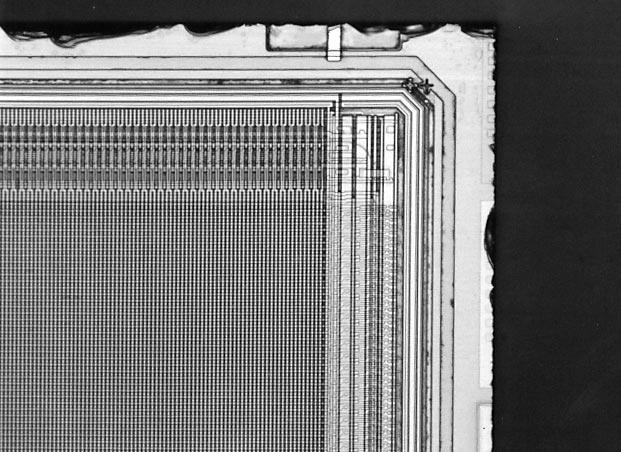
18 INDEX TO FIGURES ASSEMBLY Figures 1, 2, 6 and 7 DIE LAYOUT AND IDENTIFICATION Figures 3-5 PHYSICAL DIE STRUCTURES Figures 8-39 COLOR DRAWING OF DIE STRUCTURE Figure 28 FUSES Figures MEMORY CELL Figures ii -

19 V CC I/O V SS I/O7 I/O I/O6 I/O I/O5 I/O I/O4 N.C. V CC WE V SS CAS OE RAS 9 24 A12 A A11 A A10 A A9 A A8 A A7 A A6 V CC V SS Figure 1. Package photograph and pinout of the Hitachi ATT6 64Mbit DRAM. Mag. 4x.

20 PIN 1 Figure 2. X-ray view of the Hitachi 64Mbit DRAM. Mag. 4x.

21 Figure 3. Whole die photograph of the Hitachi 64Mbit DRAM. Mag. 12x.


22 Figure 4. Optical views of die markings. Mag. 175x.


23 Figure 5. Optical views of die corners. Mag. 200x.


24 DIE SURFACE Mag. 1300x DIE EDGE SUBSTRATE PASSIVATION CUTOUT 123 Mag. 2900x PASSIVATION 3 METAL 3 METAL 2 Mag. 7000x METAL 1 N+ Figure 6. SEM section views of the edge seal structure.


25 Au LEADFRAME Mag. 600x Au BOND PAD Mag. 680x Figure 7. SEM views of typical wirebonds. 60.


26 PASSIVATION 3 METAL 3 METAL 2 Mag. 8100x METAL 1 N+ PASSIVATION 3 METAL 3 METAL 2 METAL 1 Mag. 9000x POLY 1 POLY 1 GATE N+ S/D DELINEATION ARTIFACT PASSIVATION 3 PASSIVATION 2 PASSIVATION 1 METAL 3 IMD METAL 2 SOG glass etch, Mag. 10,500x IMD 1 METAL 1 Figure 8. SEM section views illustrating general device structure.


27 Mag. 4000x Mag. 13,500x Figure 9. Perspective SEM views illustrating final passivation coverage. 60.


28 PASSIVATION 3 PASSIVATION 2 PASSIVATION 1 METAL 3 Mag. 15,000x PASSIVATION 2 PASSIVATION 1 CAP METAL ALUMINUM BARRIER SOG Mag. 30,000x Figure 10. SEM section views of metal 3 line profiles.


29 Mag. 3100x METAL 3 Mag. 6200x Mag. 8000x VIAS Figure 11. Topological views illustrating metal 3 patterning. 0.


30 Mag. 9500x METAL 3 Mag. 25,000x METAL 2 ALUMINUM 3 Mag. 35,000x BARRIER METAL 2 Figure 12. SEM views illustrating general metal 3 integrity. 60.


31 CAP ALUMINUM BARRIER 100% THINNING METAL 2 SOG Mag. 28,500x METAL 3 IMD 2 SOG METAL 2 Mag. 25,600x Figure 13. SEM section views of metal 3-to-metal 2 vias.


32 SOG METAL 2 SOG Mag. 15,000x CAP METAL ALUMINUM BARRIER Mag. 50,000x Figure 14. SEM section views of metal 2 line profiles.


33 Mag. 5000x VIA Mag. 9000x METAL 1 METAL 2 Mag. 10,000x Figure 15. Topological SEM views of metal 2 patterning. 0.


34 METAL 2 Mag. 6000x METAL 2 Mag. 12,000x ALUMINUM Mag. 32,000x CAP BARRIER METAL 1 Figure 16. SEM views of general metal 2 integrity. 60.


35 SOG METAL 2 METAL 1 SOG Mag. 25,000x CAP ALUMINUM BARRIER 100% THINNING SOG METAL 1 Mag. 30,000x Figure 17. SEM section views of metal 2-to-metal 1 vias.


36 SOG METAL 1 Mag. 20,000x CAP W BARRIER ADHESION LAYER Mag. 55,000x Figure 18. SEM section views of metal 1 profiles.


37 Mag. 4000x decode, Mag. 5000x METAL 1 CONTACTS Mag. 5000x decode, Mag. 6000x Figure 19. Topological SEM views of metal 1 patterning. 0.


38 Mag. 9000x Mag. 15,000x TUNGSTEN Mag. 34,000x POLY 1 Figure 20. SEM views of general metal 1 integrity. 60.


39 PRE-METAL DIELECTRIC METAL 1 POLY 5 metal 1-to-poly 5, Mag. 26,500x METAL 1 POLY 3 metal 1-to-poly 3, Mag. 35,000x LOCAL OXIDE METAL 1 metal 1-to-poly 1, Mag. 33,000x POLY 1 LOCAL OXIDE Figure 21. SEM section views of metal 1-to-poly contacts.


40 SOG METAL 1 PR-METAL DIELECTRIC metal 1-to-P+, Mag. 27,500x P+ METAL 1 metal 1-to-P+, Mag. 30,000x P+ SOG METAL 1 metal 1-to-N+, Mag. 28,500x N+ Figure 22. SEM section views of metal 1-to-diffusion contacts.


41 Mag. 3200x DIFFUSION Mag. 8000x POLY 1 GATES CONTACTS Mag. 8000x POLY 1 GATES Figure 23. Topological SEM views of poly 1 patterning. 0.


42 Mag. 5000x Mag. 9000x Mag. 30,000x POLY 1 GATE Figure 24. Perspective SEM views of poly 1 coverage. 60.


43 METAL 1 PRE-METAL DIELECTRIC POLY 1 GATE P+ S/D Mag. 24,500x POLY 1 GATE P+ S/D GATE OXIDE Mag. 45,000x Figure 25. SEM section views of P-channel transistors.


44 METAL 1 POLY 1 GATE Mag. 22,500x N+ S/D POLY 1 GATE Mag. 45,000x N+ S/D GATE OXIDE SILICIDE SIDEWALL SPACER glass etch, Mag. 60,000x POLY 1 Figure 26. SEM section views of N-channel transistors.


45 METAL 1 Mag. 27,500x POLY 1 LOCAL OXIDE POLY 1 Mag. 50,000x LOCAL OXIDE GATE OXIDE Mag. 800x N-WELL DEEP N-WELL (UNDER ARRAY) P SUBSTRATE Figure 27. Section views illustrating birdsbeak profiles and well structure.
46 PASSIVATION 3 PASSIVATION 2 METAL 3 Hitachi ATT6 PASSIVATION 1 IMD 2,,,,,,,,,,,,,,,,,,,,,,,,,,,,,,, SOG,,,,,,,,,,,,,,,,,,,,, METAL 2,,,,,,,,,,,,,,,,,,,,,,,,,,,,,,,,,,,,,,,,,,,,,,,,,,,,,,,, IMD 1,,,,,,,,,,,,,,,,,,,,,,,,,,,,,,, SOG,,,, METAL 1,,,,,,,,,,,,,,,,,,,,,,,,,,,,,,,,,,,,,,,,,,,,,,,,,,, PRE-METAL DIELECTRIC,,,,,,,,,,,,,,,,,,,, SILICIDE POLY 1 P-WELL N+ S/D LOCAL OXIDE P+ S/D Orange = Nitride, Blue = Metal, Yellow = Oxide, Green = Poly, Red = Diffusion, and Gray = Substrate Figure 28. Color cross section drawing illustrating device structure. N-WELL


47 Mag. 620x BLOWN FUSES INTACT METAL 3 Mag. 1535x Figure 29. Optical views of fuse blocks.


48 INTACT BLOWN INTACT Hitachi ATT6 BLOWN intact, Mag. 4000x poly 1, Mag. 5500x INTACT BLOWN metal 3, Mag. 5500x Figure 30. Perspective SEM views of fuses. 60. BLOWN poly 1, Mag. 20,000x POLY 1


49 INTACT BLOWN Mag. 3000x BLOWN POLY 1 Mag. 12,000x Figure 31. Topological SEM views of fuses (poly 1). 0.


50 METAL 3 BLOWN PASSIVATION Hitachi ATT6 BLOWN POLY 1 Mag. 9000x METAL 3 PASSIVATION 3 PASSIVATION 1 PASSIVATION 2 Mag. 15,000x POLY 1 LOCAL OXIDE Figure 32. SEM section views of a fuse. BLOWN Mag. 17,000x


51 COMMON CAPACITOR SHEET BIT LINES Hitachi ATT6 poly 5 poly 3 INDIVIDUAL CAPACITOR PLATES WORD LINES poly 4 poly 1 Figure 33. Topological SEM views of the DRAM array, Mag. 10,000x, 0.


52 CAPACITOR SHEET Hitachi ATT6 BIT LINE poly 5 poly 3 POLY 2 CAPACITOR STEMS CAPACITOR PLATES poly 4 POLY 3 BIT LINE CONTACT Figure 34. Perspective SEM details of DRAM cells. Mag. 36,000x, 60. poly 1 WORD LINE


53 CAPACITOR SHEET poly 5 CAPACITOR PLATES C poly 4 Figure 35. Topological SEM views of DRAM cells. Mag. 30,000x, 0.


54 BIT poly 3 C WORD C Q BIT poly 1 WORD BIT Q C MEMORY ENABLE Figure 35a. Topological SEM views of DRAM cells and schematic. Mag. 30,000x, 0.


55 METAL 3 METAL 2 POLY 5 POLY 4 Mag. 11,000x POLY 1 POLY 5 SHEET POLY 4 PLATES Mag. 20,000x POLY 1 SELECT GATES POLY 5 POLY 4 Mag. 38,000x POLY 2 STEM POLY 1 Figure 36. SEM section views of DRAM cells (parallel to bit line).


56 POLY 3 BIT LINE POLY 3 BIT LINE CONTACTS Hitachi ATT6 LOCAL OXIDE POLY 1 WORD LINES N+ N+ parallel, Mag. 19,000x perpendicular, Mag. 22,000x SILICIDE POLY 5 POLY 3 POLY 3 N+ POLY 1 parallel, Mag. 38,000x POLY 3 BIT LINE Figure 37. SEM section views of poly 2 bit lines. perpendicular, glass etch, Mag. 45,000x POLY 3 BIT LINE CONTACT


57 METAL 3 POLY 5 POLY 4 Mag. 11,000x POLY 5 SHEET POLY 4 PLATE Mag. 22,000x N+ POLY 5 glass etch, Mag. 22,500x POLY 3 STEM Figure 38. SEM section views of DRAM cells (perpendicular to bit lines).


58 POLY 5 POLY 4 CAPACITOR DIELECTRIC POLY 5 POLY 4 POLY 3 POLY 2 STEM Mag. 48,000x NITRIDE Mag. 82,000x POLY 5 POLY 5 POLY 4 POLY 2 STEM POLY 3 BIT LINE POLY 3 glass etch, Mag. 48,000x glass etch, Mag. 65,000x Figure 38a. SEM section details of DRAM cells (perpendicular to bit lines).


59 POLY 5 POLY 4 Mag. 20,000x POLY 1 POLY 3 SELECT GATE NITRIDE POLY 1 SELECT GATE Mag. 46,000x LOCAL OXIDE POLY 3 glass etch, Mag. 46,000x SILICIDE LOCAL OXIDE SELECT GATE POLY 1 Figure 39. SEM section views of the poly 1 word line (perpendicular to bit lines).
Oki M A-60J 16Mbit DRAM (EDO)
") Construction Analysis Oki M5117805A-60J 16Mbit DRAM (EDO) Report Number: SCA 9707-545 Global Semiconductor Industry the Serving Since 1964 17350 N. Hartford Drive Scottsdale, AZ 85255 Phone: 602-515-9780
Construction Analysis Oki M5117805A-60J 16Mbit DRAM (EDO) Report Number: SCA 9707-545 Global Semiconductor Industry the Serving Since 1964 17350 N. Hartford Drive Scottsdale, AZ 85255 Phone: 602-515-9780
SGS-Thomson M28C K EEPROM
 Construction Analysis SGS-Thomson M28C64-121 64K EEPROM Report Number: SCA 9710-559 Global Semiconductor Industry the Serving Since 1964 17350 N. Hartford Drive Scottsdale, AZ 85255 Phone: 602-515-9780
Micron Semiconductor MT4LC16M4H9 64Mbit DRAM
 Construction Analysis Micron Semiconductor MT4LC16M4H9 64Mbit DRAM Report Number: SCA 9705-539 Global Semiconductor Industry the Serving Since 1964 15022 N. 75th Street Scottsdale, AZ 85260-2476 Phone:
Motorola MPA1016FN FPGA
 Construction Analysis Motorola MPA1016FN FPGA Report Number: SCA 9711-561 Global Semiconductor Industry the Serving Since 1964 17350 N. Hartford Drive Scottsdale, AZ 85255 Phone: 602-515-9780 Fax: 602-515-9781
NKK NR4645LQF Bit RISC Microprocessor
 Construction Analysis NKK NR4645LQF-133 64-Bit RISC Microprocessor Report Number: SCA 9707-547 Global Semiconductor Industry the Serving Since 1964 17350 N. Hartford Drive Scottsdale, AZ 85255 Phone: 602-515-9870
Motorola MC68360EM25VC Communication Controller
 Construction Analysis EM25VC Communication Controller Report Number: SCA 9711-562 Global Semiconductor Industry the Serving Since 1964 17350 N. Hartford Drive Scottsdale, AZ 85255 Phone: 602-515-9780 Fax:
UMC UM F-7 2M-Bit SRAM
 Construction Analysis UMC UM 613264F-7 2M-Bit SRAM Report Number: SCA 9609-511 Global Semiconductor Industry the Serving Since 1964 15022 N. 75th Street Scottsdale, AZ 85260-2476 Phone: 602-998-9780 Fax:
Rockwell R RF to IF Down Converter
 Construction Analysis Rockwell R6732-13 RF to IF Down Converter Report Number: SCA 9709-552 Global Semiconductor Industry the Serving Since 1964 17350 N. Hartford Drive Scottsdale, AZ 85255 Phone: 602-515-9780
DEC SA-110S StrongARM 32-Bit Microprocessor
 Construction Analysis DEC SA-110S StrongARM 32-Bit Microprocessor Report Number: SCA 9704-535 Global Semiconductor Industry the Serving Since 1964 15022 N. 75th Street Scottsdale, AZ 85260-2476 Phone:
NEC 79VR5000 RISC Microprocessor
 Construction Analysis NEC 79VR5000 RISC Microprocessor Report Number: SCA 9711-567 Global Semiconductor Industry the Serving Since 1964 17350 N. Hartford Drive Scottsdale, AZ 85255 Phone: 602-515-9780
Analog Devices ADSP KS-160 SHARC Digital Signal Processor
 Construction Analysis Analog Devices ADSP-21062-KS-160 SHARC Digital Signal Processor Report Number: SCA 9712-575 Global Semiconductor Industry the Serving Since 1964 17350 N. Hartford Drive Scottsdale,
Mosel Vitelic MS62256CLL-70PC 256Kbit SRAM
 Construction Analysis Mosel Vitelic MS62256CLL-70PC 256Kbit SRAM Report Number: SCA 9703-499 Global Semiconductor Industry the Serving Since 1964 17350 N. Hartford Drive Scottsdale, AZ 85255 Phone: 602-515-9780
Lattice 3256A-90LM PLD
 Construction Analysis PLD Report Number: SCA 9705-538 Global Semiconductor Industry the Serving Since 1964 17350 N. Hartford Drive Scottsdale, AZ 85255 Phone: 602-515-9780 Fax: 602-515-9781 e-mail: ice@ice-corp.com
Micron Semiconductor MT5C64K16A1DJ 64K x 16 SRAM
 Construction Analysis Micron Semiconductor MT5C64K16A1DJ 64K x 16 SRAM Report Number: SCA 9412-394 Global Semiconductor Industry the Serving Since 1964 17350 N. Hartford Drive Scottsdale, AZ 85255 Phone:
Dallas Semicoductor DS80C320 Microcontroller
 Construction Analysis Dallas Semicoductor DS80C320 Microcontroller Report Number: SCA 9702-525 Global Semiconductor Industry the Serving Since 1964 15022 N. 75th Street Scottsdale, AZ 85260-2476 Phone:
SGS-Thomson L4990 Controller
 Construction Analysis SGS-Thomson L4990 Controller Report Number: SCA 9710-560 Global Semiconductor Industry the Serving Since 1964 17350 N. Hartford Drive Scottsdale, AZ 85255 Phone: 602-515-9780 Fax:
Xilinx XC4036XL-1C FPGA
 Construction Analysis Xilinx XC4036XL-1C FPGA Report Number: SCA 9709-553 Global Semiconductor Industry the Serving Since 1964 17350 N. Hartford Drive Scottsdale, AZ 85255 Phone: 602-515-9780 Fax: 602-515-9781
Xilinx XC4036EX FPGA
 Construction Analysis Xilinx XC4036EX FPGA Report Number: SCA 9706-544 Global Semiconductor Industry the Serving Since 1964 15022 N. 75th Street Scottsdale, AZ 85260-2476 Phone: 602-998-9780 Fax: 602-948-1925
Lattice isplsi1032e CPLD
 Construction Analysis Lattice isplsi1032e CPLD Report Number: SCA 9612-522 Global Semiconductor Industry the Serving Since 1964 15022 N. 75th Street Scottsdale, AZ 85260-2476 Phone: 602-998-9780 Fax: 602-948-1925
SGS-Thomson M17C1001 1Mb UVEPROM
 Construction Analysis SGS-Thomson M17C1001 1Mb UVEPROM Report Number: SCA 9612-518 Global Semiconductor Industry the Serving Since 1964 15022 N. 75th Street Scottsdale, AZ 85260-2476 Phone: 602-998-9780
Motorola PC603R Microprocessor
 Construction Analysis Motorola PC603R Microprocessor Report Number: SCA 9709-551 Global Semiconductor Industry the Serving Since 1964 17350 N. Hartford Drive Scottsdale, AZ 85255 Phone: 602-515-9780 Fax:
National Semiconductor LM2672 Simple Switcher Voltage Regulator
 Construction Analysis National Semiconductor LM2672 Simple Switcher Voltage Regulator Report Number: SCA 9712-570 Global Semiconductor Industry the Serving Since 1964 17350 N. Hartford Drive Scottsdale,
Maximum MAX662 12V DC-DC Converter
 Construction Analysis Maximum MAX662 12V DC-DC Converter Report Number: SCA 9512-445 Global Semiconductor Industry the Serving Since 1964 17350 N. Hartford Drive Scottsdale, AZ 85255 Phone: 602-515-9780
Altera EPM7128SQC EPLD
 Construction Analysis Altera EPM7128SQC160-15 EPLD Report Number: SCA 9712-569 Global Semiconductor Industry the Serving Since 1964 17350 N. Hartford Drive Scottsdale, AZ 85255 Phone: 602-515-9780 Fax:
Intel Pentium Processor W/MMX
 Construction Analysis Intel Pentium Processor W/MMX Report Number: SCA 9706-540 Global Semiconductor Industry the Serving Since 1964 15022 N. 75th Street Scottsdale, AZ 85260-2476 Phone: 602-998-9780 Fax:
VTC VM365830VSJ Pre-Amp
 Construction Analysis VTC VM365830VSJ Pre-Amp Report Number: SCA 9708-549 Global Semiconductor Industry the Serving Since 1964 17350 N. Hartford Drive Scottsdale, AZ 85255 Phone: 602-515-9780 Fax: 602-515-9781
Integrated Circuit Engineering Corporation. DRAMs
 DRAMs As generally known, the focus of technology in this product category continues to be complex vertical polysilicon structures to reduce cell area. This not only pushes the limits of deposition and
Integrated Circuit Engineering Corporation EPROM
 EPROM There was lots of discussion and many technical papers covering the promises of EPROM (typically Flash) at the IEDM conference last December, but here as in the other memory areas, not much in the
Renesas M5M40R326 32Mbit DRAM Memory Structural Analysis
 August 13, 2004 Renesas M5M40R326 32Mbit DRAM Memory Structural Analysis For questions, comments, or more information about this report, or for any additional technical needs concerning semiconductor technology,
Chapter 4 : ULSI Process Integration (0.18 m CMOS Process)
") Chapter : ULSI Process Integration (0.8 m CMOS Process) Reference. Semiconductor Manufacturing Technology : Michael Quirk and Julian Serda (00). - (00). Semiconductor Physics and Devices- Basic Principles(/e)
Chapter : ULSI Process Integration (0.8 m CMOS Process) Reference. Semiconductor Manufacturing Technology : Michael Quirk and Julian Serda (00). - (00). Semiconductor Physics and Devices- Basic Principles(/e)
9/4/2008 GMU, ECE 680 Physical VLSI Design
 ECE680: Physical VLSI Design Chapter II CMOS Manufacturing Process 1 Dual-Well Trench-Isolated CMOS Process gate-oxide TiSi 2 AlCu Tungsten SiO 2 p-well poly n-well SiO 2 n+ p-epi p+ p+ 2 Schematic Layout
Lecture 030 Integrated Circuit Technology - I (5/8/03) Page 030-1
 Page 030-1") Lecture 030 Integrated Circuit Technology - I (5/8/03) Page 030-1 LECTURE 030 INTEGRATED CIRCUIT TECHNOLOGY - I (References [7,8]) Objective The objective of this presentation is: 1.) Illustrate integrated
Lecture 030 Integrated Circuit Technology - I (5/8/03) Page 030-1 LECTURE 030 INTEGRATED CIRCUIT TECHNOLOGY - I (References [7,8]) Objective The objective of this presentation is: 1.) Illustrate integrated
CMOS Technology. Flow varies with process types & company. Start with substrate selection. N-Well CMOS Twin-Well CMOS STI
 CMOS Technology Flow varies with process types & company N-Well CMOS Twin-Well CMOS STI Start with substrate selection Type: n or p Doping level, resistivity Orientation, 100, or 101, etc Other parameters
Chapter 2 Manufacturing Process
 Digital Integrated Circuits A Design Perspective Chapter 2 Manufacturing Process 1 CMOS Process 2 CMOS Process (n-well) Both NMOS and PMOS must be built in the same silicon material. PMOS in n-well NMOS
Manufacturing Process
 Digital Integrated Circuits A Design Perspective Jan M. Rabaey Anantha Chandrakasan Borivoje Nikolic Manufacturing Process July 30, 2002 1 CMOS Process 2 A Modern CMOS Process gate-oxide TiSi 2 AlCu Tungsten
ECE 659. Jan M. Rabaey Anantha Chandrakasan Borivoje Nikolic. July 30, Digital EE141 Integrated Circuits 2nd Manufacturing.
 Digital Integrated Circuits A Design Perspective Jan M. Rabaey Anantha Chandrakasan Borivoje Nikolic Manufacturing Process July 0, 00 1 CMOS Process 1 A Modern CMOS Process gate-oxide TiSi AlCu Tungsten
Manufacturing Process
 CMOS Manufacturing Process CMOS Process 1 A Modern CMOS Process gate-oxide TiSi AlCu Tungsten SiO n+ p-well p-epi poly n-well p+ SiO p+ Dual-Well Trench-Isolated CMOS Process Circuit Under Design V DD
EE BACKEND TECHNOLOGY - Chapter 11. Introduction
 1 EE 212 FALL 1999-00 BACKEND TECHNOLOGY - Chapter 11 Introduction Backend technology: fabrication of interconnects and the dielectrics that electrically and physically separate them. Aluminum N+ Early
CMOS Manufacturing Process
 CMOS Manufacturing Process CMOS Process A Modern CMOS Process gate-oxide TiSi 2 AlCu Tungsten SiO 2 n+ p-well p-epi poly n-well p+ SiO 2 p+ Dual-Well Trench-Isolated CMOS Process Circuit Under Design V
Semiconductor Manufacturing Technology. IC Fabrication Process Overview
 Semiconductor Manufacturing Technology Michael Quirk & Julian Serda October 00 by Prentice Hall Chapter 9 IC Fabrication Process Overview /4 Objectives After studying the material in this chapter, you
1 Thin-film applications to microelectronic technology
 1 Thin-film applications to microelectronic technology 1.1 Introduction Layered thin-film structures are used in microelectronic, opto-electronic, flat panel display, and electronic packaging technologies.
CMOS FABRICATION. n WELL PROCESS
 CMOS FABRICATION n WELL PROCESS Step 1: Si Substrate Start with p- type substrate p substrate Step 2: Oxidation Exposing to high-purity oxygen and hydrogen at approx. 1000 o C in oxidation furnace SiO
ECE520 VLSI Design. Lecture 7: CMOS Manufacturing Process. Payman Zarkesh-Ha
 ECE520 VLSI Design Lecture 7: CMOS Manufacturing Process Payman Zarkesh-Ha Office: ECE Bldg. 230B Office hours: Wednesday 2:00-3:00PM or by appointment E-mail: pzarkesh@unm.edu Slide: 1 Review of Last
Packaging and Ball Bonding Gold wire makes contact from bonding pads on chip to package Gold wire is formed into ball to make contact Uses an
 Packaging and Ball Bonding Gold wire makes contact from bonding pads on chip to package Gold wire is formed into ball to make contact Uses an ultrasonic process & heat Process called "Ball Bonding" Wedge
Microelectronics. Integrated circuits. Introduction to the IC technology M.Rencz 11 September, Expected decrease in line width
 Microelectronics Introduction to the IC technology M.Rencz 11 September, 2002 9/16/02 1/37 Integrated circuits Development is controlled by the roadmaps. Self-fulfilling predictions for the tendencies
CMOS Manufacturing process. Design rule set
 CMOS Manufacturing process Circuit design Set of optical masks Fabrication process Circuit designer Design rule set Process engineer All material: Chap. 2 of J. Rabaey, A. Chandrakasan, B. Nikolic, Digital
Plasma Etching Rates & Gases Gas ratios affects etch rate & etch ratios to resist/substrate
 Plasma Etching Rates & Gases Gas ratios affects etch rate & etch ratios to resist/substrate Development of Sidewalls Passivating Films Sidewalls get inert species deposited on them with plasma etch Creates
ECE321 Electronics I
 ECE321 Electronics I Lecture 19: CMOS Fabrication Payman Zarkesh-Ha Office: ECE Bldg. 230B Office hours: Tuesday 2:00-3:00PM or by appointment E-mail: payman@ece.unm.edu Slide: 1 Miller Effect Interconnect
EE 330 Lecture 9. IC Fabrication Technology Part II. -Oxidation -Epitaxy -Polysilicon -Planarization -Resistance and Capacitance in Interconnects
 EE 330 Lecture 9 IC Fabrication Technology Part II -Oxidation -Epitaxy -Polysilicon -Planarization -Resistance and Capacitance in Interconnects Review from Last Time Etching Dry etch (anisotropic) SiO
Lecture 200 BiCMOS Technology (12/12/01) Page 200-1
 Page 200-1") Lecture 200 BiCMOS Technology (12/12/01) Page 200-1 LECTURE 200 BICMOS TECHNOLOGY (READING: Text-Sec. 2.11) INTRODUCTION Objective Illustrate BiCMOS technology Outline Introduction Physical process illustration
Lecture 200 BiCMOS Technology (12/12/01) Page 200-1 LECTURE 200 BICMOS TECHNOLOGY (READING: Text-Sec. 2.11) INTRODUCTION Objective Illustrate BiCMOS technology Outline Introduction Physical process illustration
Chapter 3 CMOS processing technology
 Chapter 3 CMOS processing technology (How to make a CMOS?) Si + impurity acceptors(p-type) donors (n-type) p-type + n-type => pn junction (I-V) 3.1.1 (Wafer) Wafer = A disk of silicon (0.25 mm - 1 mm thick),
W Metallization in a 3-D Memory
 W Metallization in a 3-D Memory December 8, 2005 Michael Konevecki, Usha Raghuram, Victoria Eckert, Vance Dunton, Brad Herner & Steve Radigan 3-D Memory Cells Matrix memory cells consist of a memory element
EE 560 FABRICATION OF MOS CIRCUITS. Kenneth R. Laker, University of Pennsylvania
 1 EE 560 FABRICATION OF MOS CIRCUITS 2 CMOS CHIP MANUFACTRING STEPS Substrate Wafer Wafer Fabrication (diffusion, oxidation, photomasking, ion implantation, thin film deposition, etc.) Finished Wafer Wafer
VLSI Design and Simulation
 VLSI Design and Simulation CMOS Processing Technology Topics CMOS Processing Technology Semiconductor Processing How do we make a transistor? Fabrication Process Wafer Processing Silicon single crystal
We are moving to 155 Donner Lab From Thursday, Feb 2 We will be able to accommodate everyone!
 -Spring 006 Digital Integrated Circuits Lecture 4 CMOS Manufacturing Process Design Rules EECS141 1 Good News! We are moving to 155 Donner Lab From Thursday, Feb We will be able to accommodate everyone!
Chapter 3 Silicon Device Fabrication Technology
 Chapter 3 Silicon Device Fabrication Technology Over 10 15 transistors (or 100,000 for every person in the world) are manufactured every year. VLSI (Very Large Scale Integration) ULSI (Ultra Large Scale
Complementary Metal Oxide Semiconductor (CMOS)
") Technische Universität Graz Institute of Solid State Physics Complementary Metal Oxide Semiconductor (CMOS) Franssila: Chapters 26,28 Technische Universität Graz Institute of Solid State Physics Complementary
Technische Universität Graz Institute of Solid State Physics Complementary Metal Oxide Semiconductor (CMOS) Franssila: Chapters 26,28 Technische Universität Graz Institute of Solid State Physics Complementary
Plasma Etching Rates & Gases Gas ratios affects etch rate & etch ratios to resist/substrate
 Plasma Etching Rates & Gases Gas ratios affects etch rate & etch ratios to resist/substrate Development of Sidewalls Passivating Films Sidewalls get inert species deposited on them with plasma etch Creates
Technology. Semiconductor Manufacturing. Hong Xiao INTRODUCTION TO SECOND EDITION SPIE PRESS
 INTRODUCTION TO Semiconductor Manufacturing Technology SECOND EDITION Hong Xiao TECHNISCHE INFORMATIONSBiBUOTHEK UNIVERSITATSBIBLIOTHEK HANNOVER SPIE PRESS Bellingham,Washington USA Contents Preface to
10 Manor Parkway, Suite C Salem, New Hampshire
 Micro-Precision Technologies (MPT) is an independent manufacturer of hybrid integrated circuits, multichip modules, and high-precision thick film substrates for the military, medical, avionics, optoelectronics,
Chapter 4 Fabrication Process of Silicon Carrier and. Gold-Gold Thermocompression Bonding
 Chapter 4 Fabrication Process of Silicon Carrier and Gold-Gold Thermocompression Bonding 4.1 Introduction As mentioned in chapter 2, the MEMs carrier is designed to integrate the micro-machined inductor
PROCESS FLOW AN INSIGHT INTO CMOS FABRICATION PROCESS
 Contents: VI Sem ECE 06EC63: Analog and Mixed Mode VLSI Design PROCESS FLOW AN INSIGHT INTO CMOS FABRICATION PROCESS 1. Introduction 2. CMOS Fabrication 3. Simplified View of Fabrication Process 3.1 Alternative
CX Thin Fil s. Resistors Attenuators Thin-Film Products Thin-Film Services. ISO 9001:2008 RoHS/REACH Compliant ITAR Compliant
 CX Thin Fil s Resistors Attenuators Thin-Film Products Thin-Film Services www.cxthinfilms.com ISO 9001:2008 RoHS/REACH Compliant ITAR Compliant www.cxthinfilms.com sales@cxthinfilms.com +1 (401) 461-5500
Fairchild Semiconductor Application Note June 1983 Revised March 2003
 Fairchild Semiconductor Application Note June 1983 Revised March 2003 High-Speed CMOS (MM74HC) Processing The MM74HC logic family achieves its high speed by utilizing microcmos Technology. This is a 3.5
ECSE 6300 IC Fabrication Laboratory Lecture 8 Metallization. Die Image
 ECSE 6300 IC Fabrication Laboratory Lecture 8 Metallization Prof. Rensselaer Polytechnic Institute Troy, NY 12180 Office: CII-6229 Tel.: (518) 276-2909 e-mails: luj@rpi.edu http://www.ecse.rpi.edu/courses/s18/ecse
Lecture 1A: Manufacturing& Layout
 Introduction to CMOS VLSI Design Lecture 1A: Manufacturing& Layout David Harris Harvey Mudd College Spring 2004 Steven Levitan Fall 2008 1 The Manufacturing Process For a great tour through the IC manufacturing
Beam Leads. Spider bonding, a precursor of TAB with all-metal tape
 Beam Leads The vast majority of chips are intended for connection with thermosonic bonds: all other methods require some modification to the wafer. As early as 1972, Jordan described three gang-bonding
UT Austin, ECE Department VLSI Design 2. CMOS Fabrication, Layout Rules
 2. CMOS Fabrication, Layout, Design Rules Last module: Introduction to the course How a transistor works CMOS transistors This module: CMOS Fabrication Design Rules CMOS Fabrication CMOS transistors are
EE 434 Lecture 9. IC Fabrication Technology
 EE 434 Lecture 9 IC Fabrication Technology Quiz 7 The layout of a film resistor with electrodes A and B is shown. If the sheet resistance of the film is 40 /, determine the resistance between nodes A and
Manufacturing Process
 Manufacturing Process 1 CMOS Process 2 A Modern CMOS Process gate-oxide TiSi 2 AlCu Tungsten SiO 2 n+ p-well p-epi poly n-well p+ SiO 2 p+ Dual-Well Trench-Isolated CMOS Process 3 Single-crystal ingot
ASIM-X MEMS-Specific Design Rules
 ASIM-X MEMS-Specific Design Rules Version 2 Revised April 5, 2006. This is a beta version, subject to change. Revised by G. K. Fedder, Carnegie Mellon University. 1 Process Overview ASIM-X, an acronym
Nonplanar Metallization. Planar Metallization. Professor N Cheung, U.C. Berkeley
 Nonplanar Metallization Planar Metallization Passivation Metal 5 (copper) Metal 3 (copper) Interlevel dielectric (ILD) Via (tungsten) Metal 1 (copper) Tungsten Plug to Si Silicon Caps and Plugs oxide oxide
CS/ECE 5710/6710. N-type Transistor. N-type from the top. Diffusion Mask. Polysilicon Mask. CMOS Processing
 CS/ECE 5710/6710 CMOS Processing Addison-Wesley N-type Transistor D G +Vgs + Vds S N-type from the top i electrons - Diffusion Mask Mask for just the diffused regions Top view shows patterns that make
Mark T. Bohr Intel Senior Fellow, Technology and Manufacturing Group Director, Process Architecture and Integration INTEL CORPORATION
 Mark T. Bohr Intel Senior Fellow, Technology and Manufacturing Group Director, Process Architecture and Integration INTEL CORPORATION Patents» 6762464, N-P butting connections on SOI substrates, 7/13/2004.»
CMOS Processing Technology
 CHAPTER 2 CMOS Processing Technology Outline 2 1. CMOS Technologies 2. Layout Design Rules 3. CMOS Process Enhancements 4. Technology-related CAD Issues 5. Manufacturing Issues CMOS Technologies 3 n-well
Challenges of Fan-Out WLP and Solution Alternatives John Almiranez
 Challenges of Fan-Out WLP and Solution Alternatives John Almiranez Advanced Packaging Business Development Asia Introduction to Fan-Out WLP Introduction World of mobile gadgetry continues to rapidly evolve
CMOS Processing Technology
 CHAPTER 2 CMOS Processing Technology Outline 2 1. CMOS Technologies 2. Layout Design Rules 3. CMOS Process Enhancements 4. Technology-related CAD Issues 5. Manufacturing Issues CMOS Technologies 3 n-well
Improvement of Laser Fuse Processing of Fine Pitch Link Structures for Advanced Memory Designs
 Improvement of Laser Fuse Processing of Fine Pitch Link Structures for Advanced Memory Designs Joohan Lee, Joseph J. Griffiths, and James Cordingley GSI Group Inc. 60 Fordham Rd. Wilmington, MA 01887 jlee@gsig.com
Silicon Wafer Processing PAKAGING AND TEST
 Silicon Wafer Processing PAKAGING AND TEST Parametrical test using test structures regularly distributed in the wafer Wafer die test marking defective dies dies separation die fixing (not marked as defective)
Cost of Integrated Circuits
 Cost of IC Design 1 Cost of Integrated Circuits NRE (Non-Recurrent Engineering) costs fixed design time and effort, mask generation independent of sales volume / number of products one-time cost factor
Regents of the University of California
 Topography Issues Degradation of lithographic resolution PR step coverage, streaking Thickness differences pose problems for reduction steppers Direction of Spin PR PR PR Stringers Problematic when using
Lecture 22: Integrated circuit fabrication
 Lecture 22: Integrated circuit fabrication Contents 1 Introduction 1 2 Layering 4 3 Patterning 7 4 Doping 8 4.1 Thermal diffusion......................... 10 4.2 Ion implantation.........................
IC Fabrication Technology Part III Devices in Semiconductor Processes
 EE 330 Lecture 10 IC Fabrication Technology Part III Metalization and Interconnects Parasitic Capacitances Back-end Processes Devices in Semiconductor Processes Resistors Diodes Review from Last Lecture
EE CMOS TECHNOLOGY- Chapter 2 in the Text
 1 EE 212 FALL 1999-00 CMOS TECHOLOGY- Chapter 2 in the Text In this set of notes we will describe a modern CMOS process flow. In the simplest CMOS technologies, we need to realize simply MOS and MOS transistors
CHAPTER - 4 CMOS PROCESSING TECHNOLOGY
 CHAPTER - 4 CMOS PROCESSING TECHNOLOGY Samir kamal Spring 2018 4.1 CHAPTER OBJECTIVES 1. Introduce the CMOS designer to the technology that is responsible for the semiconductor devices that might be designed
Fabrication and Layout
 Fabrication and Layout Kenneth Yun UC San Diego Adapted from EE271 notes, Stanford University Overview Semiconductor properties How chips are made Design rules for layout Reading Fabrication: W&E 3.1,
Silicon Epitaxial CVD Want to create very sharp PN boundary grow one type layer on other in single crystal form High dopant layers on low dopant
 Silicon Epitaxial CVD Want to create very sharp PN boundary grow one type layer on other in single crystal form High dopant layers on low dopant substrate Creates latch up protection for CMOS Buried Epi
Process Integration. NMOS Generic NMOS Process Flow. CMOS - The MOSIS Process Flow
 Process Integration Self-aligned Techniques LOCOS- self-aligned channel stop Self-aligned Source/Drain Lightly Doped Drain (LDD) Self-aligned silicide (SALICIDE) Self-aligned oxide gap MEMS Release Techniques
EE 330 Lecture 9. IC Fabrication Technology Part 2
 EE 330 Lecture 9 IC Fabrication Technology Part 2 Quiz 8 A 2m silicon crystal is cut into wafers using a wire saw. If the wire diameter is 220um and the wafer thickness is 350um, how many wafers will this
FABRICATION of MOSFETs
 FABRICATION of MOSFETs CMOS fabrication sequence -p-type silicon substrate wafer -creation of n-well regions for pmos transistors, -impurity implantation into the substrate. -thick oxide is grown in the
Silicon Epitaxial CVD Want to create very sharp PN boundary grow one type layer on other in single crystal form High dopant layers on low dopant
 Silicon Epitaxial CVD Want to create very sharp PN boundary grow one type layer on other in single crystal form High dopant layers on low dopant substrate Creates latch up protection for CMOS Buried Epi
Lect. 2: Basics of Si Technology
 Unit processes Thin Film Deposition Etching Ion Implantation Photolithography Chemical Mechanical Polishing 1. Thin Film Deposition Layer of materials ranging from fractions of nanometer to several micro-meters
Is Now Part of To learn more about ON Semiconductor, please visit our website at
 Is Now Part of To learn more about ON Semiconductor, please visit our website at www.onsemi.com ON Semiconductor and the ON Semiconductor logo are trademarks of Semiconductor Components Industries, LLC
SCMOS Layout Rules - Well
 SCMOS Layout s - Well 1.1 Minimum width 12 3.6 1.2 Minimum spacing between wells at different potential 18 5.4 1.3 Minimum spacing between wells at same potential 6 1.8 1.4 Minimum spacing between wells
This Appendix discusses the main IC fabrication processes.
 IC Fabrication B B.1 Introduction This Appendix discusses the main IC fabrication processes. B.2 NMOS fabrication NMOS transistors are formed in a p-type substrate. The NMOS fabrication process requires
II. A. Basic Concept of Package.
 Wafer Level Package for Image Sensor Module Won Kyu Jeung, Chang Hyun Lim, Jingli Yuan, Seung Wook Park Samsung Electro-Mechanics Co., LTD 314, Maetan3-Dong, Yeongtong-Gu, Suwon, Gyunggi-Do, Korea 440-743
Isolation Technology. Dr. Lynn Fuller
 ROCHESTER INSTITUTE OF TECHNOLOGY MICROELECTRONIC ENGINEERING Isolation Technology Dr. Lynn Fuller Motorola Professor 82 Lomb Memorial Drive Rochester, NY 14623-5604 Tel (585) 475-2035 Fax (585) 475-5041
Regents of the University of California 1
 Electroplating: Metal MEMS Nickel Surface-Micromachining Process Flow Photoresist Wafer Release Etchant Use electroplating to obtain metal μstructures When thick: call it LIGA Pros: fast low temp deposition,
TSV Processing and Wafer Stacking. Kathy Cook and Maggie Zoberbier, 3D Business Development
 TSV Processing and Wafer Stacking Kathy Cook and Maggie Zoberbier, 3D Business Development Outline Why 3D Integration? TSV Process Variations Lithography Process Results Stacking Technology Wafer Bonding
Automotive Electronics Council Component Technical Committee
 ATTACHMENT 1 AEC - Q100-001 REV-C WIRE BOND SHEAR TEST Acknowledgment Any document involving a complex technology brings together experience and skills from many sources. The Automotive Electronics Counsel