QUANTUM DOTS AND NANOWIRES: FABRICATION AND CHARACTERIZATION
|
|
|
- Veronica Gibbs
- 6 years ago
- Views:
Transcription

1 Research Article QUANTUM DOTS AND NANOWIRES: FABRICATION AND CHARACTERIZATION Virk H. S.* Address for correspondence Nanotechnology Laboratory, DAV Institute of Engineering & Technology, Kabir Nagar, Jalandhar , India ABSTRACT Quantum Dots and Nanowires have emerged as backbone of 21 st century industry based on nanotechnology. A variety of nanofabrication techniques have emerged during the last two decades like atomic deposition, chemical methods, chemical self assembly, cluster methods and lithographic techniques. However, the electrochemical method involving the electro-deposition of metals/semiconductors into etched pores of Ion Track filters/membranes is a simple and convenient technique. Template synthesis of Quantum Dots and Nanowires has been achieved by using anodic alumina membranes and polymer membranes of pore diameter varying from nm. The copper nanowire micrographs show non-uniformities in growth. Using Reverse Micelle technique, nanorods of Barium carbonate and Barium oxalate were synthesized along with nanocrystals of Iron oxalate. Cadmium sulphide nanocrystals and needles have been grown using micro-emulsion technique with different co-surfactants. Characterization of grown nanostructures has been done by using SEM, TEM and XRD. KEYWORDS Quantum dots, Nanowires, Electrodeposition, Template, Reverse micelles. INTRODUCTION In recent years, one of the most active areas of research has been nanotechnology (1). Quantum dots (0D), also known as nanocrystals, are a special class of materials known as semiconductors, which are crystals composed of periodic groups of II-VI, III-V, or IV-VI materials. Quantum dots are unique class of semiconductors because they are so small, ranging from 2-10 nanometers (10-50 atoms) in diameter. At these small sizes materials behave differently, giving quantum dots unprecedented tunability and enabling never before seen applications to science and technology. Nanowires/nanorods (1D) have attracted considerable attention in recent years (2, 3) because of their novel physical properties and potential applications as interconnects in nanometre-scale electronics. The progress in this field has been accelerated by advances in both synthetic methods of preparing the nanoporous templates, and development
2 of techniques capable of filling the pores of such membranes. Examples of long aspect ratio nanoporous membranes include nanochannel glass membranes, anodized aluminium substrates, and various polymeric membranes. Filling of the pores of such membranes with long aspect ratio nanowires/nanorods has been accomplished by electrodeposition, high- pressure metal melt injection, and photochemical methods. Many methods have been developed for the fabrication of copper nanowires but template synthesis (4) is considered to be most suitable and useful for growth of nanowires. Electrochemical deposition route is easy, low-cost as well as less cumbersome compared to other fabrication techniques. Electrochemical cell used in electrodeposition of copper into pores of anodic alumina template was fabricated in our laboratory. Nanocrystalline semiconductor materials such as PbS, CdS and ZnS have attracted considerable attention due to their unique properties which are missing in bulk materials. CdS, in particular, has been extensively studied due to its potential applications in field effect transistors (FETS), light emitting diodes (LEDs), photocatalysis and biological sensors (5-7). This study is undertaken to develop fabrication techniques for quantum dots and naowires to exploit their application in nanodevices. MATERIALS AND METHODS Anodic Alumina Membrane (AAM) manufactured by Whatman Company has been used to grow quantum dots and nanowires by electrodeposition technique. The pore size selected varies from 20 nm to 200 nm. The electrochemical cell fabricated in our laboratory was used to grow copper nanowires of 200 nm using an electrolyte with a composition of 20gm/100 ml CuSO 4.5H 2 O + 25% of dilute H 2 SO 4 at room temperature. Electrodeposition of copper nanowires depends on many factors, namely, interelectrode spacing, electrolyte composition and ph value, current density and time of deposition. To achieve uniform deposition of nanowires, templates were cleaned in the ultrasonic bath for 10 minutes. After cleaning, the templates were fixed to the adhesive copper tape to make it a perfect cathode. The copper nanowires were liberated from their host AAM matrix by
3 dissolving it in 1M NaOH at room temperature (22 0 C) for 2 hours. The copper nanowires grown on copper foils were dried in an oven at 50 0 C for 30 minutes. The cleaned and dried nanowires were mounted on aluminium stubs with the help of double adhesive tape, coated with a layer of gold palladium alloy in Jeol Sputter JFC 1100 and viewed under Scanning Electron Microscope (Jeol, JSM-6100) at an accelerating voltage of 20 kv. Fig.1 (a, b) shows SEM micrographs of electrodeposited copper nanowires of 200 nm diameter and length of a few microns. We also followed chemical route to nanotechnology using Reverse Micelle technique (8, 9) of microemulsions to grow nanorods and nanodots/quantum dots of some metals. The mechanism for the formation of nanocrystalline material using reverse micelles may be understood qualitatively by considering the synthesis of a simple compound like metal oxalate and carbonate. Microemulsion. A should be metal ion and B should be oxalate in case of metal oxalate and in case of metal carbonate B should be carbonate. These two microemulsions are mixed by constant stirring and the droplets continuously collide, which results in the interchange of reactants. During this process, the reaction takes place inside the nanoreactor. In microemulsion system, the reverse micelles of metal and oxalate/carbonate forms the fused dimer which finally breaks down into two stable smaller droplets because surface tension becomes high due to large surface area and dimmer is unable to sustain its geometry. RESULTS AND DISCUSSION Copper nanowires were examined under SEM under different magnifications. Fig. 1(a) shows a typical cross-sectional view of copper nanowires grown in alumina template. Fig. 1(b) represents the lateral view of nanowires. Obviously, the diameter of copper nanowires is identical to the diameter of pores (200 nm) of anodisc. Nanowires are quite uniform but they are not perfect cylinders. It has been reported (10) that pore diameters of commercially available templates vary over a large range. The aspect ratio, that is, the ratio of length to diameter, is on the order of 300.
. The cross-sectional and lateral views are somewhat distorted and not as smooth as in case of anodisc alumina templates.")
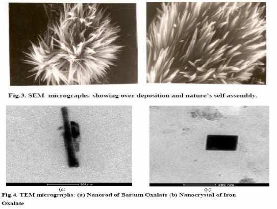
4 Electrodeposition of copper nanowires was achieved in polycarbonate template under identical conditions. The polymer template was dissolved in dichloromethane at room temperature. SEM micrographs of grown copper nanowires are shown in Fig. 2(a,b). The cross-sectional and lateral views are somewhat distorted and not as smooth as in case of anodisc alumina templates. The diameter of copper nanowires matches with the pore diameter (100 nm) of polycarbonate template. We also performed electrodepostion in 20 nm pore diameter alumina template. Due to over deposition of copper into nanopores, we failed to grow copper nanowires. Instead, what we achieved was a pattern resembling some botanical plant species depicting nature s self assembly (Fig.3). It is reported (11) that over deposition of copper may also lead to metallic microrose having petals in nanometer dimensions
5
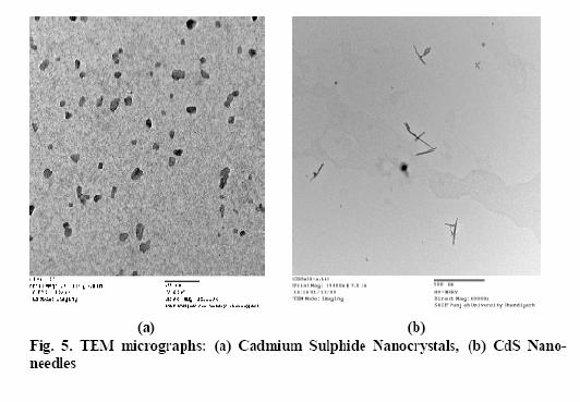
6 Our second line of attack has been the chemical route of Reverse Micelle technique (12). Transmission Electron Microscope (200 kv FEI, Amsterdam) micrographs of nanorods of Barium carbonate and naocrystals of Iron oxalate prepared in our laboratory are shown in Fig. 4(a,b). Cadmium sulphide nanocrystals and nano-needles have also been fabricated using chemical route as shown by TEM micrographs in Fig. 5(a,b). CONCLUSIONS Our preliminary investigations confirm that electrodeposition of copper nanowires in anodic alumina and polycarbonate templates are the simplest route to nanotechnology. The diameter of copper nanowires matches with the pore diameter of templates. Structure and morphology of copper nanowires reveals its polycrystalline nature. Nanorods/needles and nanodots/crystals fabricated by reverse micelle technique are going to be tested for future applications in nanodevices. ACKNOWLEDGEMENT The author is thankful to the Principal DAV Institute of Engineering & Technology, Jalandhar and DAV College Managing Committee, New Delhi for providing a grant of Rs. 50 lacs to set up Nanotechnology Research Centre in DAVIET, Jalandhar. The help of research staff of the research centre in preparation of samples is duly acknowledged. REFERENCES 1. Ratner M and Ratner D, Nanotechnology: A gentle introduction to the next big idea, Pearson Education Publication, London, 2003; G Z Cao, Nanostructures and Nanomaterials, London:Imperial College Press, Sarkar J, Khan G G and Basumallick A, Bull. Mater. Sci., 30(3), 271 (2007). 3. Sun Shin H, Song J Y and Yu J, Materials Letters, 63, 397 (2009). 4. Virk H S, Kishore K and Baloria V, J. Nano Res., 10, 63 (2010). 5. Alivisatos A P, Science, 271, 933 (1996). 6. Kolvin V L, et al., Nature, 370, 354 (1994). 7. Klein D L, et al, Nature, 389, 699 (1997). 8. Ganguli A K and Ahmad T, J. Nanoscience and Nanotechnology, 7, 2029 (2007). 9. Ahmed J, Vaidya S, Ahmed T, Sujatha Devi P, Das D and Ganguli A, Mater. Res. Bull., 43, 264 (2008). 10. Schonenberger C, Van der Zande B M I, Fokkink L G J, Henry M, Schmid C, Kniger M, Bachtold A, Huher R, Birk H and Stairfer V, J. Phys. Chem. B, 101, 5497 (1997). 11. Kumar S, Kumar V, Sharma M L and Chakarvarti, S K, Superlattices and Microstructures, 43, 324(2008). 12. Ahmad T and Ganguli A K, J. Am. Ceram. Soc., 89, 1326 (2006).
International Journal of Advanced Engineering Technology E-ISSN
 Research Article TEMPLATE GROWTH OF COPPER NANOWIRES AND EXOTIC PATTERNS OF METALLIC COPPER USING ELECTRODEPOSITION TECHNIQUE VIRK H. S.* Address for Correspondence Nanotechnology Laboratory, DAV Institute
Simple fabrication of highly ordered AAO nanotubes
 Journal of Optoelectronic and Biomedical Materials Volume 1, Issue 1, March 2009, p. 79-84 Simple fabrication of highly ordered AAO nanotubes N. Taşaltin a, S. Öztürk a, H. Yüzer b, Z. Z. Öztürk a,b* a
THE INFLUENCE OF SUBSTRATE PREPARATION, ANODIZATION CONDITIONS AND POST ANODIZING TREATMENT ON AAO MICROSTRUCTURE. Eva JINDROVÁ, Vít JAN, Jan ČUPERA
 THE INFLUENCE OF SUBSTRATE PREPARATION, ANODIZATION CONDITIONS AND POST ANODIZING TREATMENT ON AAO MICROSTRUCTURE Eva JINDROVÁ, Vít JAN, Jan ČUPERA Brno University of Technology, Faculty of Mechanical
Fabrication of Highly Ordered Gold Nanorods Film Using Alumina Nanopores
 JNS 2 (2012) 235-240 Fabrication of Highly Ordered Gold Nanorods Film Using Alumina Nanopores Z. Soltani a,*, M. Moradi b, M. Noormohammadi b, F. Behzadi b a Department of Physics, Shiraz Branch, Islamic
Study on the influence on the formation of highly ordered porous anodic aluminia membrane
 Study on the influence on the formation of highly ordered porous anodic aluminia membrane O Pong-Sik, Ryang Se-Hun, Sin Gum-Chol, Hwang Guk-Nam, Hong Yong-Son * Kim Hyong Jik Normal University, Pyongyang,
light Specific- Power CdTe Thin-Film Solar Cells using Quantum Dots Development of Highly Efficiency, Ultra-light
 Development of Highly Efficiency, Ultra-light light Weight, Radiation-Resistant, Resistant, High-Specific Specific- Power CdTe Thin-Film Solar Cells using Quantum Dots Neelkanth G. Dhere Florida Solar
Fabrication and Structural Studies of Porous Anodic Oxide Film on Pure Aluminium and Aluminium Alloy (AA 1100)
") http://www.e-journals.in Chemical Science Transactions DOI:10.7598/cst2014.726 2014, 3(2), 556-561 RESEARCH ARTICLE Fabrication and Structural Studies of Porous Anodic Oxide Film on Pure Aluminium and
http://www.e-journals.in Chemical Science Transactions DOI:10.7598/cst2014.726 2014, 3(2), 556-561 RESEARCH ARTICLE Fabrication and Structural Studies of Porous Anodic Oxide Film on Pure Aluminium and
Properties of nanostructures obtained by anodization of aluminum in phosphoric acid at moderate potentials
 Properties of nanostructures obtained by anodization of aluminum in phosphoric acid at moderate potentials L Zaraska, G D Sulka 1 and M Jaskuła Department of Physical Chemistry & Electrochemistry, Jagiellonian
Development of New Generation Of Coatings with Strength-Ductility Relationship, Wear, Corrosion and Hydrogen Embrittlement Resistance Beyond the
 Development of New Generation Of Coatings with Strength-Ductility Relationship, Wear, Corrosion and Hydrogen Embrittlement Resistance Beyond the Current Materials Accomplishments till date As the structural
DC electrochemical deposition of CdSe nanorods array using porous anodic aluminum oxide template
 Materials Science and Engineering A303 (2001) 19 23 www.elsevier.com/locate/msea DC electrochemical deposition of CdSe nanorods array using porous anodic aluminum oxide template Cheng-min Shen, Xiao-gang
GROWTH AND CHARACTERIZATION OF NANOSTRUCTURED CdS THIN FILMS BY CHEMICAL BATH DEPOSITION TECHNIQUE
 Chalcogenide Letters Vol. 6, No. 8, September 29, p. 415 419 GROWTH AND CHARACTERIZATION OF NANOSTRUCTURED CdS THIN FILMS BY CHEMICAL BATH DEPOSITION TECHNIQUE V. B. SANAP *, B. H. PAWAR, * MSS s College
Selective growth of Au nanograins on specific positions (tips, edges. heterostructures.
 Selective growth of Au nanograins on specific positions (tips, edges and facets) of Cu 2 O octahedrons to form Cu 2 O-Au hierarchical heterostructures. Han Zhu b, MingLiang Du* a,b, DongLiang Yu b, Yin
Investigation on the effect of Electro-co-deposition process parameter bath temperature on Nano Structured Ni-WC Composite coating properties
 International Journal of Materials Science ISSN 0973-4589 Volume 11, Number 1 (2016), pp. 9-15 Research India Publications http://www.ripublication.com Investigation on the effect of Electro-co-deposition
Novel concept of rechargeable battery using iron oxide nanorods. anode and nickel hydroxide cathode in aqueous electrolyte
 Supplementary Information for: Novel concept of rechargeable battery using iron oxide nanorods anode and nickel hydroxide cathode in aqueous electrolyte Zhaolin Liu *, Siok Wei Tay and Xu Li Institute
Supporting Information
 Supporting Information Shaping Up: Spontaneous Formation of Ordered Mesoscopic Salt Bowls Katla Sai Krishna, a,# Bosukonda V. V. S. Pavan Kumar a and Muthusamy Eswaramoorthy a,* a Nanomaterials and Catalysis
Hierarchical 3D ZnCo 2 O 4 Nanowire Arrays/Carbon Cloth Anodes for A Novel Class of High-Performance Flexible Lithium-ion Batteries
 Supporting Information Hierarchical 3D ZnCo 2 O 4 Nanowire Arrays/Carbon Cloth Anodes for A Novel Class of High-Performance Flexible Lithium-ion Batteries Bin Liu, Jun Zhang, Xianfu Wang, Gui Chen, Di
Fabrication of Highly Ordered Al 2 O 3 Nanohole Arrays As a Nanostructured Template
 Fabrication of Highly Ordered Al 2 O 3 Nanohole Arrays As a Nanostructured Template Jie Gong, Bill Butler and Giovanni Zangari Materials Science Program University of Alabama at Tuscaloosa This work was
The Effect of Electrolyte Temperature on Formation of Porous Aluminium Oxide Films in Anodising Process
 Special Issue for International Conference of Advanced Materials Engineering and Technology (ICAMET 2013), 28-29 November 2013, Bandung Indonesia AENSI Journals Advances in Environmental Biology Journal
ScienceDirect. Formation of Cu and Ni Nanowires by Electrodeposition
 Available online at www.sciencedirect.com ScienceDirect Procedia Materials Science 8 (2015 ) 617 622 International Congress of Science and Technology of Metallurgy and Materials, SAM - CONAMET 2013 Formation
Fabrication and Characterization of a Polypyrrole Coated Copper Nanowire Gas Sensor
 Fabrication and Characterization of a Polypyrrole Coated Copper Nanowire Gas Sensor A.B.Kashyout*, H. Shokry Hassan*, A. A. A. Nasser**, I. Morsy**, and H. Abuklill** *Advanced Technology and New Materials
The Improvement in Energy Efficiency Based on Nano-structure Materials
 International Workshop on 1iGO Science and Technology 2010 The Improvement in Energy Efficiency Based on Nanostructure Materials Chien Chon Chen Department of Energy and Resources, National United University,
Fabrication and optical absorption of ordered indium oxide nanowire arrays embedded in anodic alumina membranes
 9 February 2001 Chemical Physics Letters 334 (2001) 298±302 www.elsevier.nl/locate/cplett Fabrication and optical absorption of ordered indium oxide nanowire arrays embedded in anodic alumina membranes
FORMATION OF PLATELET STRUCTURE CARBON NANO- AND MICRO-FIBERS BY TEMPLATE METHOD
 FORMATION OF PLATELET STRUCTURE CARBON NANO- AND MICRO-FIBERS BY TEMPLATE METHOD Hidetaka Konno 1, Shin ya Sato 1, Hiroki Habazaki 1, Michio Inagaki 2 1 Graduate School of Engineering, Hokkaido University,
LiNi 0.5 Mn 1.5 O 4 porous nanorods as high-rate and long-life cathode for Li-ion batteries
 Supporting Information LiNi 0.5 Mn 1.5 O 4 porous nanorods as high-rate and long-life cathode for Li-ion batteries Xiaolong Zhang, Fangyi Cheng, Jingang Yang, Jun Chen* Key Laboratory of Advanced Energy
QUANTUM SIZE EFFECT IN CHEMOSYNTHESIZED NANOSTRUCTURED CdS THIN FILMS
 Digest Journal of Nanomaterials and Biostructures Vol. 5, No 4, October-December 2010, p. 805-810 QUANTUM SIZE EFFECT IN CHEMOSYNTHESIZED NANOSTRUCTURED CdS THIN FILMS S. A. VANALAKAR, S. S. MALI, M. P.
Journal of Chemical and Pharmaceutical Research, 2017, 9(1): Research Article
: Research Article") Available online www.jocpr.com Journal of Chemical and Pharmaceutical Research, 2017, 9(1):163-167 Research Article ISSN : 0975-7384 CODEN(USA) : JCPRC5 Synthesis and Characterization of Carbon Nano Spheres
Available online www.jocpr.com Journal of Chemical and Pharmaceutical Research, 2017, 9(1):163-167 Research Article ISSN : 0975-7384 CODEN(USA) : JCPRC5 Synthesis and Characterization of Carbon Nano Spheres
MEMS technology for production of different micro- and nanodevices
 P6.4 MEMS technology for production of different micro- and nanodevices A.M. Kudanovich, N.I. Mukhurov, L.R. Paleuskaya, Y.V. Mironchyk Laboratory of Micro- Electronics, Mechanics and Sensorics, Institute
A study on the growth of TiO 2 nanorods using sol electrophoresis
 JOURNAL OF MATERIALS SCIENCE 39 (2 004)895 901 A study on the growth of TiO 2 nanorods using sol electrophoresis S. J. LIMMER, T. P. CHOU, G. Z. CAO University of Washington, Department of Materials Science
Investigation into Electrospun LaMnO 3 Nanofibres
 Universities Research Journal 2011, Vol. 4, No. 4 Investigation into Electrospun LaMnO 3 Nanofibres Zin Min Myat 1, Than Than Win 2 and Yin Maung Maung 3 Abstract This paper aims to prepare nanofibres
magnetic nanoparticles, part 1. synthetic methods: from mechanochemistry to biomimetics
 magnetic nanoparticles, part 1. synthetic methods: from mechanochemistry to biomimetics Tanya Prozorov, Ph.D. US DOE Ames Laboratory e mail: tprozoro@ameslab.gov 1 outline some definitions what happens
Ibn Al-Haitham Jour. for Pure & Appl. Sci Vol. 32 (1) 2019
 2019") Novel Co-Precipitation Method for Synthesis of Nanostructured Nickel Oxide in Accordance to PH: Structural and Optical Properties as an Active Optical Filter Zehraa N. Abdul-Ameer Lecturer Remote Sensing
Novel Co-Precipitation Method for Synthesis of Nanostructured Nickel Oxide in Accordance to PH: Structural and Optical Properties as an Active Optical Filter Zehraa N. Abdul-Ameer Lecturer Remote Sensing
Synthesis, Characterization and Optical Properties of ZnS Thin Films
 Synthesis, Characterization and Optical Properties of ZnS Thin Films H. R. Kulkarni KJ College of Engineering and Management Research, Pune, India Abstract: ZnS thin films were prepared by pulsed electrodeposition
PREPARATION OF NEODYMIUM HYDROXIDE NANORODS AND NEODYMIUM OXIDE NANORODS BY A HYDROTHERMAL METHOD
 Digest Journal of Nanomaterials and Biostructures Vol. 10, No. 2, April - June 2015, p. 715-719 PREPARATION OF NEODYMIUM HYDROXIDE NANORODS AND NEODYMIUM OXIDE NANORODS BY A HYDROTHERMAL METHOD N. EKTHAMMATHAT
Supporting Information for. A Water-in-Salt Electrolyte for Potassium-Ion Batteries
 Supporting Information for A Water-in-Salt Electrolyte for Potassium-Ion Batteries Daniel P. Leonard #, Zhixuan Wei #, Gang Chen, Fei Du *, Xiulei Ji * Department of Chemistry, Oregon State University,
Mater. Res. Soc. Symp. Proc. Vol Materials Research Society
 Mater. Res. Soc. Symp. Proc. Vol. 940 2006 Materials Research Society 0940-P13-12 A Novel Fabrication Technique for Developing Metal Nanodroplet Arrays Christopher Edgar, Chad Johns, and M. Saif Islam
CHAPTER-VII SUMMARY AND CONCLUSIONS
 CHAPTER-VII SUMMARY AND CONCLUSIONS Chapter-VII Summary and Conclusions Sr. No. Title Page No. 7.1 Summary 167 7.2 Conclusions.. 171 CHAPTER SEVEN Summary and Conclusions 7.1: Summary The technologies
Hydrothermal Synthesis of Zinc Oxide Nanowires on Kevlar using ALD and Sputtered ZnO Seed Layers
 Hydrothermal Synthesis of Zinc Oxide Nanowires on Kevlar using ALD and Sputtered ZnO Seed Layers Ashley D. Mason 1, Todd J. Waggoner 1, Sean W. Smith 1, John F. Conley Jr. 1, Brady J. Gibbons 2, Derryl
6th International Conference on Advanced Design and Manufacturing Engineering (ICADME 2016)
") 6th International Conference on Advanced Design and Manufacturing Engineering (ICADME 2016) Porous Co3O4 irregular Micro-cubes with lithium storage performances Ting Wanga, Hao Zhengb, Jinsong Chengc,
6th International Conference on Advanced Design and Manufacturing Engineering (ICADME 2016) Porous Co3O4 irregular Micro-cubes with lithium storage performances Ting Wanga, Hao Zhengb, Jinsong Chengc,
Metallization deposition and etching. Material mainly taken from Campbell, UCCS
 Metallization deposition and etching Material mainly taken from Campbell, UCCS Application Metallization is back-end processing Metals used are aluminum and copper Mainly involves deposition and etching,
Carbon Science and Technology
 ASI Carbon Science and Technology ARTICLE (Advanced Non-Carbon Materials) Received: 01/07/2013, Accepted: 29/07/2013 ------------------------------------------------------------------------------------------------------------------------------
Synthesis and Characterization of Zinc Iron Sulphide (ZnFeS) Of Varying Zinc Ion Concentration
 Of Varying Zinc Ion Concentration") International Journal of Science and Technology Volume 5 No. 5, May, 2016 Synthesis and Characterization of Zinc Iron Sulphide (ZnFeS) Of Varying Zinc Ion Concentration I. B. Obasi 1 and J. C. Osuwa 2
International Journal of Science and Technology Volume 5 No. 5, May, 2016 Synthesis and Characterization of Zinc Iron Sulphide (ZnFeS) Of Varying Zinc Ion Concentration I. B. Obasi 1 and J. C. Osuwa 2
EFFECT OF GROWTH TEMPERATURE ON THE CATALYST-FREE GROWTH OF LONG SILICON NANOWIRES USING RADIO FREQUENCY MAGNETRON SPUTTERING
 International Journal of Nanoscience Vol. 10, Nos. 1 & 2 (2011) 13 17 #.c World Scienti c Publishing Company DOI: 10.1142/S0219581X11007594 EFFECT OF GROWTH TEMPERATURE ON THE CATALYST-FREE GROWTH OF LONG
THE EFFECTS OF ANODIZING CONDITION AND POST TREATMENT ON THE GROWTH OF NICKEL NANOWIRES USING ANODIC ALUMINUM OXIDE
 THE EFFECTS OF ANODIZING CONDITION AND POST TREATMENT ON THE GROWTH OF NICKEL NANOWIRES USING ANODIC ALUMINUM OXIDE M. T. Safarzadeh 1, A. Arab 2 and S. M. A. Boutorabi 2,3,* * boutorabi@iust.ac.ir Received:
PARAMETER EFFECTS FOR THE GROWTH OF THIN POROUS ANODIC ALUMINUM OXIDES
 10.1149/1.2794473, The Electrochemical Society PARAMETER EFFECTS FOR THE GROWTH OF THIN POROUS ANODIC ALUMINUM OXIDES S. Yim a, C. Bonhôte b, J. Lille b, and T. Wu b a Dept. of Chem. and Mat. Engr., San
Studies on Structural and Optical Properties of Iron doped Cds Nanoparticles ABSTRACT
 Studies on Structural and Optical Properties of Iron doped Cds Nanoparticles Atheek P., Vidhya M. and Balasundaram O. N Department of Physics, PSG College of Arts & Science, Coimbatore, Tamil Nadu, India
A Parametric Study on the Electrodeposition of Copper Nanocrystals on a Gold Film Electrode. Andrea Harmer Co-op term #1 April 25, 2003
 A Parametric Study on the Electrodeposition of Copper Nanocrystals on a Gold Film Electrode Andrea Harmer Co-op term #1 April 25, 2003 Outline of Presentation: Introduction Purpose General method Parameters:
Simple method for formation of nanometer scale holes in membranes. E. O. Lawrence Berkeley National Laboratory, Berkeley, CA 94720
 Simple method for formation of nanometer scale holes in membranes T. Schenkel 1, E. A. Stach, V. Radmilovic, S.-J. Park, and A. Persaud E. O. Lawrence Berkeley National Laboratory, Berkeley, CA 94720 When
The effects of Fe/Al 2 O 3 preparation technique as a catalyst on synthesized CNTs in CVD method.
 Science Journal of Physics Science Journal Publication Science Journal of Physics Web: http://www.sjpublication.com/sjp.html The effects of Fe/Al 2 O 3 preparation technique as a catalyst on synthesized
Synthesis and Characterization of Cadmium Sulfide (CdS) Quantum Dots (QDS) for Quantum Dot Sensitized Solar Cell Applications
 Quantum Dots (QDS) for Quantum Dot Sensitized Solar Cell Applications") Nano Vision, Vol. 5(7-9), 237-241, July-September 2015 (An International Research Journal of Nano Science & Technology), www.nano-journal.org ISSN 2231-2579 (Print) ISSN 2319-7633 (Online) Synthesis and
Nano Vision, Vol. 5(7-9), 237-241, July-September 2015 (An International Research Journal of Nano Science & Technology), www.nano-journal.org ISSN 2231-2579 (Print) ISSN 2319-7633 (Online) Synthesis and
b
 Solid State Phenomena Vols. 121-123 (2007) pp 441-444 Online: 2007-03-15 (2007) Trans Tech Publications, Switzerland doi:10.4028/www.scientific.net/ssp.121-123.441 Controlled Synthesis of BaF 2 Nanorods
Rapid electroplating of Cu coatings by mechanical attrition method
 Rapid electroplating of Cu coatings by mechanical attrition method NING Zhao-hui( 宁朝晖 ), HE Ye-dong( 何业东 ) Beijing Key Laboratory for Corrosion, Erosion and Surface Technology, University of Science and
Supporting Information
 Supporting Information Designing hybrid NiP 2/NiO nanorod arrays for efficient alkaline hydrogen evolution Meng-Ying Wu, Peng-Fei Da, Tong Zhang, Jing Mao,*, Hui Liu,*, and Tao Ling,*, Key Laboratory for
Synthesis and Characterization of Cadmium Sulfide Nanoparticles
 Synthesis and Characterization of Cadmium Sulfide Nanoparticles R.Hepzi Pramila Devamani 1*, R.Kiruthika, P.Mahadevi and S.Sagithapriya 2 1 1. Assistant Professor, Department of Physics, V.V.Vanniaperumal
Growth and Micro-structural Study of Bismuth Antimony Telluride for Thermoelectric Applications
 International Journal of Mechanics Structural. ISSN 0974-312X Volume 7, Number 1 (2017), pp. 1-5 International Research Publication House http://www.irphouse.com Growth and Micro-structural Study of Bismuth
Supporting Information
 Electronic Supplementary Material (ESI) for Nanoscale. This journal is The Royal Society of Chemistry 2014 Supporting Information Experimental All the chemicals were of analytical grade and used without
Synthesis of Nanostructures by Electrochemical Processing
 Synthesis of Nanostructures by Electrochemical Processing Giovanni Zangari, Robert M. Metzger, Bill Butler University of Alabama at Tuscaloosa The work presented was partly sponsored through DOD grant
J. Mater. Sci. Technol., 2010, 26(11),
,") J. Mater. Sci. Technol., 2010, 26(11), 1016-1020. Effects of Current Density on the Microstructure and the Corrosion Resistance of Alumina Coatings Embedded with SiC Nano-particles Produced by Micro-arc
J. Mater. Sci. Technol., 2010, 26(11), 1016-1020. Effects of Current Density on the Microstructure and the Corrosion Resistance of Alumina Coatings Embedded with SiC Nano-particles Produced by Micro-arc
The effect of pulsed electrodeposition parameters on the microstructure and magnetic properties of the CoNi nanowires
 JNS 1 (2012) 249-255 The effect of pulsed electrodeposition parameters on the microstructure and magnetic properties of the CoNi nanowires M. Almasi Kashi *, A. Ramazani, N. Akhshi, E. J. Khamse, Z. Fallah
Supporting Information. Controlling the Morphology of Rhodium Nanocrystals by Manipulating the Growth Kinetics with a Syringe Pump
 Supporting Information Controlling the Morphology of Rhodium Nanocrystals by Manipulating the Growth Kinetics with a Syringe Pump Hui Zhang,, Weiyang Li, Mingshang Jin, Jie Zeng, Taekyung Yu, Deren Yang,
ELECTRIDEPOSITION AND WEAR BEHAVIOR OF NANO-STRUCTURED Cr-WC COMPOSITE COATINGS FROM A TRIVALENT CHROMIUM BATH
 2nd International Conference on Ultrafine Grained & Nanostructured Materials (UFGNSM) International Journal of Modern Physics: Conference Series Vol. 5 (2012) 737 743 World Scientific Publishing Company
Microstructured Optical Fibers as New Nanotemplates for High Pressure CVD
 Mater. Res. Soc. Symp. Proc. Vol. 988 2007 Materials Research Society 0988-QQ04-02 Microstructured Optical Fibers as New Nanotemplates for High Pressure CVD Neil Baril 1, John Badding 1, Pier Savio 2,
Gold nanorods grown on microgels leading to hexagonal nanostructures
 1 Supporting information for the paper: Gold nanorods grown on microgels leading to hexagonal nanostructures V. R. Rajeev Kumar, A. K. Samal, T. S. Sreeprasad and T. Pradeep* DST Unit on Nanoscience (DST-UNS),
Structure and optical properties of M/ZnO (M=Au, Cu, Pt) nanocomposites
 nanocomposites") Solar Energy Materials & Solar Cells 8 () 339 38 Structure and optical properties of M/ (M=Au, Cu, Pt) nanocomposites U. Pal a,b, *, J. Garc!ıa-Serrano a, G. Casarrubias-Segura a, N. Koshizaki c, T. Sasaki
Solar Energy Materials & Solar Cells 8 () 339 38 Structure and optical properties of M/ (M=Au, Cu, Pt) nanocomposites U. Pal a,b, *, J. Garc!ıa-Serrano a, G. Casarrubias-Segura a, N. Koshizaki c, T. Sasaki
Cubic CeO 2 Nanoparticles as Mirror-like Scattering Layer for Efficient Light Harvesting in Dye-Sensitized Solar Cells
 Supplementary Material (ESI for Chemical Communications This journal is (c The Royal Society of Chemistry 2011 Supplementary Material (ESI for Chemical Communications Cubic CeO 2 Nanoparticles as Mirror-like
Remote Access Laboratory Guide
 Remote Access Laboratory Guide Electrodeposition of Nickel Nanowires In this exercise, you will: Understand the process of electroplating and its use at the nanoscale. Describe the function of a template
Characterization of cupper iodine thin films fabricate by spin coating from nanoparticles produced by exploding Cu wire in Iodine solution
 International Journal of ChemTech Research CODEN (USA): IJCRGG, ISSN: 0974-4290, ISSN(Online):2455-9555 Vol.10 No.9, pp 1109-1116, 2017 Characterization of cupper iodine thin films fabricate by spin coating
EFFECTS OF CURRENT DENSITY ON SIZE AND SURFACE MORPHOLOGY OF HIGH SPEED DIRECT NANO-CRYSTALLINE NICKEL PLATING ON TITANIUM SURFACE
 EFFECTS OF CURRENT DENSITY ON SIZE AND SURFACE MORPHOLOGY OF HIGH SPEED DIRECT NANO-CRYSTALLINE NICKEL PLATING ON TITANIUM SURFACE Noor Zaimah 1, Azieyanti Nurain 1 and Sakhawat Hussain 2 1 Department
EFFECT OF DIFFERENT FERROUS CONCENTRATION ON STRUCTURAL AND MECHANICAL PROPERTIES OF ELECTRODEPOSITED FeNiCo THIN FILMS
 EFFECT OF DIFFERENT FERROUS CONCENTRATION ON STRUCTURAL AND MECHANICAL PROPERTIES OF ELECTRODEPOSITED FeNiCo THIN FILMS K. Mohan Rangam Kadiresan 1,V. Senthil Kumar 2 1 Research Scholar, 2 Associate Professor,
METAL FINISHING. (As per revised VTU syllabus: )
") METAL FINISHING (As per revised VTU syllabus: 2015-16) Definition: It is a process in which a specimen metal (article) is coated with another metal or a polymer in order to modify the surface properties
METAL FINISHING (As per revised VTU syllabus: 2015-16) Definition: It is a process in which a specimen metal (article) is coated with another metal or a polymer in order to modify the surface properties
Controllable Growth of Semiconductor Heterostructures Mediated by Bifunctional Ag 2 S Nanocrystals as Catalyst or Source-Host
 Controllable Growth of Semiconductor Heterostructures Mediated by Bifunctional Ag 2 S Nanocrystals as Catalyst or Source-Host Guoxing Zhu and Zheng Xu Nanjing National Laboratory of Solid State Microstructure,
Supplementary information for Titanate nanofunnel brushes: toward functional interfacial applications,
 Supplementary information for Titanate nanofunnel brushes: toward functional interfacial applications, by Kenji Okada, Yasuaki Tokudome, Paolo Falcaro, Yuichiro Takamatsu, Atsushi Nakahira and Masahide
Superionic Solid State Stamping (S4)
") Superionic Solid State Stamping (S4) Lead Faculty Researcher: Placid Ferreira Department: Materials Science & Engineering Hsu et al, Nano Letters, 2007 1. Description: This dry, single step, electrochemical
Superionic Solid State Stamping (S4) Lead Faculty Researcher: Placid Ferreira Department: Materials Science & Engineering Hsu et al, Nano Letters, 2007 1. Description: This dry, single step, electrochemical
Defense Technical Information Center Compilation Part Notice
 UNCLASSIFIED Defense Technical Information Center Compilation Part Notice ADP012154 TITLE: Structural Characterization of GaN Nanowires Fabricated via Direct Reaction of Ga Vapor and Ammonia DISTRIBUTION:
Polycrystalline Silicon Produced by Joule-Heating Induced Crystallization
 Polycrystalline Silicon Produced by Joule-Heating Induced Crystallization So-Ra Park 1,2, Jae-Sang Ro 1 1 Department of Materials Science and Engineering, Hongik University, Seoul, 121-791, Korea 2 EnSilTech
Water used in all experiments was the Milli-Q (18.2MΩ) water. Silver nanoparticles were
 water. Silver nanoparticles were") Supplementary Methods Synthesis of Ag nanoparticle. AgNO 3 (ACS regent, 99%), Polyvinyl pyrrolidone (PVP, Mw = 55000) and glycol (EG, Vetetc TM reagent grade, 98%) were purchased from Sigma-Aldrich. Water
Supplementary Methods Synthesis of Ag nanoparticle. AgNO 3 (ACS regent, 99%), Polyvinyl pyrrolidone (PVP, Mw = 55000) and glycol (EG, Vetetc TM reagent grade, 98%) were purchased from Sigma-Aldrich. Water
Zinc Oxide Tetrapod Impregnated with Platinum for Ethanol Sensor
 CMU. J.Nat.Sci. Special Issue on Nanotechnology (2008) Vol. 7(1) 159 Zinc Oxide Tetrapod Impregnated with Platinum for Ethanol Sensor Chawalit Bhoomanee, Pamika Phunsod, Atcharawan Gardchareon, Pongsri
General Introduction to Microstructure Technology p. 1 What is Microstructure Technology? p. 1 From Microstructure Technology to Microsystems
 General Introduction to Microstructure Technology p. 1 What is Microstructure Technology? p. 1 From Microstructure Technology to Microsystems Technology p. 9 The Parallels to Microelectronics p. 15 The
Nanjing University, Nanjing , P.R.China, 2. Max-Planck-Institut für Mikrostrukturphysik, Weinberg 2, D Halle, Germany
 Solid State Phenomena Vol. 16 (25) pp. 41-46 online at http://www.scientific.net 25 Trans Tech Publications, Switzerland Microstructural Characterization of BaTiO 3 Ceramic Nanoparticles Synthesized by
CORROSION PROTECTION OF IRON USING COMPOSITE COATINGS BASED ON ZINC AND ZINC ALLOYS
 MK0400057 CORROSION PROTECTION OF IRON USING COMPOSITE COATINGS BASED ON. CORROSION PROTECTION OF IRON USING COMPOSITE COATINGS BASED ON ZINC AND ZINC ALLOYS G. Raichevski*, N. Boshkov*, D. Koleva*, Ch.
Microstructure-dependent oxidation-assisted dealloying of Cu0.7Al0.3
 Microstructure-dependent oxidation-assisted dealloying of Cu0.7Al0.3 thin films Jiangbin Su 1,2,*, Meiping Jiang 1, Honghong Wang 1, Yang Liu 1 1. Experiment Center of Electronic Science and Technology
The application of nano metal powder
 The application of nano metal powder Nano material and nanotechnology respectively belong to the new material and advanced technology that emerged in the late 20 th century. Due to the small size effect,
Seeing is Believing. - Nanostructure of Anodic Alumina Film - The International Hard Anodizing Association 15th Technical Symposium
 Seeing is Believing - Nanostructure of Anodic Alumina Film - The International Hard Anodizing Association 15th Technical Symposium September 24-26, 2014 Sheraton Lincoln Harbor Hotel, Weehawken, NJ Sachiko
Ceramic Processing Research
 Journal of Ceramic Processing Research. Vol. 9, No. 6, pp. 678~682 (2008) J O U R N A L O F Ceramic Processing Research Jondo Yun a, *, Chunsheng Du b and Nigel Browning c a Department of Nano Science
MTT- 601 Engineering Materials 2L - 1T 0P/3Cr Ceramic materials Polymeric Materials Composite materials: References:
 MTT- 601 Engineering Materials 2L - 1T 0P/3Cr Ferrous alloys as engineering materials. Steel for automotive, building, naval and structural applications. High performance steels. New generation cast irons
Research Article Fabrication of a Zinc Aluminum Oxide Nanowire Array Photoelectrode for a Solar Cell Using a High Vacuum Die Casting Technique
 Photoenergy, Article ID 302075, 5 pages http://dx.doi.org/10.1155/2014/302075 Research Article Fabrication of a Zinc Aluminum Oxide Nanowire Array Photoelectrode for a Solar Cell Using a High Vacuum Die
Supplementary Information
 Supplementary Information Fabrication of (001)-oriented monoclinic WO 3 films on FTO substrates Jin You Zheng, Guang Song, Chang Woo Kim and Young Soo Kang* Korea Center for Artificial Photosynthesis (KCAP),
Three-dimensional Nano-electrode. by Metal-Nanowire-Nonwoven Clothes
 Supporting Information for Three-dimensional Nano-electrode by Metal-Nanowire-Nonwoven Clothes Makoto Kawamori,* Takahiro Asai, Yoshimasa Shirai, Shunsuke Yagi, Masatsugu Oishi, Tetsu Ichitsubo, and Eiichiro
CURRICULUM VITAE. Solid State Physics (PG-II) ACADEMIC AWARDS:
 ACADEMIC AWARDS:") Dr. RABINDRA NATH GAYEN Assistant Professor Department of Physics Presidency University 86/1 College Street Kolkata - 700073. e-mail: rabin.physics@presiuniv.ac.in rabin.gayen@gmail.com Phone No: +91-9836754743
Dr. RABINDRA NATH GAYEN Assistant Professor Department of Physics Presidency University 86/1 College Street Kolkata - 700073. e-mail: rabin.physics@presiuniv.ac.in rabin.gayen@gmail.com Phone No: +91-9836754743
Growth of monocrystalline In 2 O 3 nanowires by seed orientation dependent vapour-solid-solid mechanism
 Electronic Supplementary Material (ESI) for Journal of Materials Chemistry C. This journal is The Royal Society of Chemistry 2014 Electronic Supplementary Information (ESI) Growth of monocrystalline In
Supporting Information for
 Supporting Information for Hollow Carbon Nanofiber-Encapsulated Sulfur Cathodes for High Specific Capacity Rechargeable Lithium Batteries Guangyuan Zheng, Yuan Yang, Judy J. Cha, Seung Sae Hong and Yi
SYNTHESIS OF MANGANESE OXIDE NANOSTRUCTURES ON CARBON PAPER FOR SUPERCAPACITOR APPLICATIONS
 Surface Review and Letters, Vol. 16, No. (9) 513 517 c World Scientific Publishing Company SYNTHESIS OF MANGANESE OXIDE NANOSTRUCTURES ON CARBON PAPER FOR SUPERCAPACITOR APPLICATIONS M. A. MASTRO,,C.R.EDDYJr.andF.KUB
Large-Size Liftable Inverted-Nanobowl Sheets as Reusable Masks for Nanolithiography
 Large-Size Liftable Inverted-Nanobowl Sheets as Reusable Masks for Nanolithiography NANO LETTERS 2005 Vol. 5, No. 9 1784-1788 Xudong Wang, Changshi Lao, Elton Graugnard, Christopher J. Summers, and Zhong
PHYchip Corporation. SCU Nanotechnology Course presentation. Dhaval Brahmbhatt President & CEO. Friday, April 29 th, 2005
 SCU Nanotechnology Course presentation Dhaval Brahmbhatt President & CEO Friday, April 29 th, 2005, San Jose, CA 95110. 1 Course Books (1) Primary Book: Introduction to Nanoscale Science and Technology
Mechanical and magnetic properties of nanostructured CoNiP films
 PRAMANA c Indian Academy of Sciences Vol. 67, No. 2 journal of August 2006 physics pp. 341 349 Mechanical and magnetic properties of nanostructured CoNiP films R N EMERSON 1, C JOSEPH KENNADY 2, and S
Synthesis, Structural, Optical and Electrical Properties of Cadmium sulphide Thin Films by Chemical Bath Deposition Method
 International Journal of ChemTech Research CODEN (USA): IJCRGG ISSN : 0974-4290 Vol.6, No.7, pp 3748-3752, Sept-Oct 2014 Synthesis, Structural, Optical and Electrical Properties of Cadmium sulphide Thin
Formation mechanism of alumina nanotube array
 Physics Letters A 309 (2003) 109 113 www.elsevier.com/locate/pla Formation mechanism of alumina nanotube array Y.F. Mei a,x.l.wu a,,x.f.shao a,g.s.huang a,g.g.siu b a National Laboratory of Solid State
Dr. Arun Singh. Sponsored by DST. Year of start. Held. Principal Investigator. Principal Investigator BOYSCAST FELLOW
 Dr. Arun Singh Advanced Electronic and Nano-Materials Laboratory R.N.- 304 III Floor, Department of Physics Faculty of Natural Sciences Jamia Millia Islamia, Central University, New Delhi-110025 (INDIA).
Chapter -3 RESULTS AND DISCSSION
 Chapter -3 RESULTS AND DISCSSION 3.1. INTRODUCTION In nanotechnology, an iron oxide nanoparticle, is defined as a small object that behaves as a whole unit in terms of its transport and properties. Particles
Available online Journal of Scientific and Engineering Research, 2016, 3(1): Research Article
: Research Article") Available online www.jsaer.com, 2016, 3(1):68-73 Research Article ISSN: 2394-2630 CODEN(USA): JSERBR Incorporation of Super Fine Particles in Ni-P Deposits on Low Carbon Steel Abdalwahid Kadhim Rajih 1,
Available online www.jsaer.com, 2016, 3(1):68-73 Research Article ISSN: 2394-2630 CODEN(USA): JSERBR Incorporation of Super Fine Particles in Ni-P Deposits on Low Carbon Steel Abdalwahid Kadhim Rajih 1,
Electrical Characterization of Nanocrystalline CdS Thin Films in PVA Matrix.
 Volume: 3 Issue: 2 030 036 Electrical Characterization of Nanocrystalline CdS Thin Films in PVA Matrix. Ankita R. Karule Dept. of Science and Humanities, Government Polytechnic, Amravati, India. e-mail: