Today s agenda (19-JAN-2010)
|
|
|
- Eugene Edwards
- 6 years ago
- Views:
Transcription
1 Today s agenda (19-JAN-2010) 1) Overview of Integrated Circuit technology 2) Managing Deadlines 3) A Spring Schedule 4) Suggested milestones 5) Project concept presentations
2 Action items from last time First priority is to choose a project (today) Drives choice of technology Helps me choose supplemental material Few minute oral (or PPT) presentation Will need to sign NDAs for MOSIS Establish which computer going to use Get set-up with an account on our server 2
3 ASIC vs PCB Assumption is experience with Printed Circuit Board design Schematic capture Layout, DRC Artwork generation Rework (sometimes) possible Application Specific Integrated Circuit Schematic capture Simulation (parasitics matter!) Layout, DRC Post layout simulation (parasitics matter!) Layout Versus schematicerat Artwork generation Rework impossible* 3
4 Courtesy UT Austin HISTORY 19 th Century - Solid-State Rectifiers Application of Crystal Detector in Radio Sets BJT Constructed by Bardeen and Brattain 1959 Integrated Circuit Constructed by Kilby 4

5 Semiconductor Manufacturing Process 5
 Wafer Manufacturing c) Crystal structure 2.")
6 Semiconductor Manufacturing Process Fundamental Processing Steps 1.Silicon Manufacturing a) Czochralski method. b) Wafer Manufacturing c) Crystal structure 2.Photolithography a) Photoresists b) Photomask and Reticles c) Patterning 6
 Oxide Growth & Deposition b) Oxide Removal c) Other effects d) Local Oxidation 4.")
7 Semiconductor Manufacturing Process (cont) 3.Oxide Growth & Removal a) Oxide Growth & Deposition b) Oxide Removal c) Other effects d) Local Oxidation 4. Diffusion & Ion Implantation a) Diffusion b) Other effects c) Ion Implantation 7
8 Silicon Manufacturing Crystal Growth and Wafer Manufacturing 8
9 FABRICATING SILICON Quartz, or Silica, Consists of Silicon Dioxide Sand Contains Many Tiny Grains of Quartz Silicon Can be Artificially Produced by Combining Silica and Carbon in Electric Furnice Gives Polycrystalline Silicon (multitude of crystals) Practical Integrated Circuits Can Only be Fabricated from Single-Crystal Material 9


10 CRYSTAL GROWTH Czochralski Process is a Technique in Making Single-Crystal Silicon A Solid Seed Crystal is Rotated and Slowly Extracted from a Pool of Molten Si Requires Careful Control to Give Crystals Desired Purity and Dimensions 10

11 CYLINDER OF MONOCRYSTALLINE The Silicon Cylinder is Known as an Ingot Typical Ingot is About 1 or 2 Meters in Length Can be Sliced into Hundreds of Smaller Circular Pieces Called Wafers Each Wafer Yields Hundreds or Thousands of Integrated Circuits 11


12 WAFER MANUFACTURING The Silicon Crystal is Sliced by Using a Diamond-Tipped Saw into Thin Wafers Sorted by Thickness Damaged Wafers Removed During Lapping Etch Wafers in Chemical to Remove any Remaining Crystal Damage Polishing Smoothes Uneven Surface Left by Sawing Process 12


13 THE CRYSTAL STRUCTURE OF SILICON A Unit Cell Has 18 Silicons Atoms Weak Bonding Along Cleavage Planes Wafer Splits into 4 or 6 Wedge-Shaped Fragments Miller Indices are Used to Assign to Each Possible Plane Passing Through the Crystal Lattice 13
14 Silicon Manufacturing Photolithography 14

15 Photolithography Photolithography is a technique that is used to define the shape of micromachined structures on a wafer. 15
16 Photolithography Photoresist The first step in the photolithography process is to develop a mask, which will be typically be a chromium pattern on a glass plate. Next, the wafer is then coated with a polymer which is sensitive to ultraviolet light called a photoresist. Afterward, the photoresist is then developed which transfers the pattern on the mask to the photoresist layer. 16
17 Photolithography Photoresist There are two basic types of Photoresists Positive and Negative. Positive resists. Positive resists decomposes ultraviolet light. The resist is exposed with UV light wherever the underlying material is to be removed. In these resists, exposure to the UV light changes the chemical structure of the resist so that it becomes more soluble in the developer. The exposed resist is then washed away by the developer solution, leaving windows of the bare underlying material. The mask, therefore, contains an exact copy of the pattern which is to remain on the wafer. 17
18 Photolithography Photoresist Negative resists Exposure to the UV light causes the negative resist to become polymerized, and more difficult to dissolve. Therefore, the negative resist remains on the surface wherever it is exposed, and the developer solution removes only the unexposed portions. Masks used for negative photoresists, therefore, contain the inverse (or photographic "negative") of the pattern to be transferred. 18
19 Photolithography Model Figure 1a shows a thin film of some material (eg, silicon dioxide) on a substrate of some other material (eg, a silicon wafer). Photoresist layer (Figure 1b ) Ultraviolet light is then shone through the mask onto the photoresist (figure 1c). 19
20 Photolithography Model (cont) The photoresist is then developed which transfers the pattern on the mask to the photoresist layer (figure 1d). A chemical (or some other method) is then used to remove the oxide where it is exposed through the openings in the resist (figure 1e). Finally the resist is removed leaving the patterned oxide (figure 1f). 20

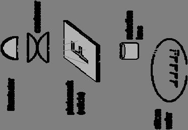
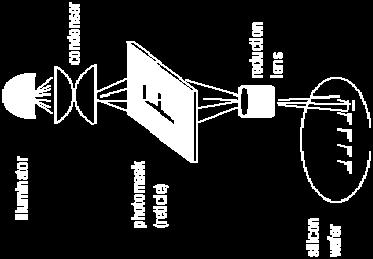
21 Photolithography Photomasks and Reticles Photomask This is a square glass plate with a patterned emulsion of metal film on one side. The mask is aligned with the wafer, so that the pattern can be transferred onto the wafer surface. Each mask after the first one must be aligned to the previous pattern. 21
22 Photolithography Photomasks and Reticles When a image on the photomask is projected several times, side by side onto the wafer, this is known as stepping and the photomask is called a reticle. An common reticle is the 5X The patterns on the 5X reticle are reduced 5 times when projected onto the wafer. This means the dies on the photomask are 5 times larger than they are on the final product. There are other kinds of reduction reticles (2X, 4X, and 10X), but the 5X is the most commonly used. Reduction reticles are used on a variety of steppers, the most common being ASM, Canon, Nikon, and GCA. 22
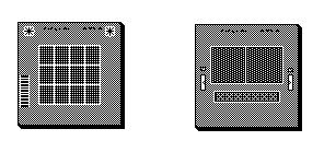
23 Photolithography Photomasks and Reticles Examples of 5X Reticles: 23
24 Photolithography Photomasks and Reticles Once the mask has been accurately aligned with the pattern on the wafer's surface, the photoresist is exposed through the pattern on the mask with a high intensity ultraviolet light. There are three primary exposure methods: contact, proximity, and projection. 24
25 Photolithography Patterning The last stage of Photolithography is a process called ashing. This process has the exposed wafers sprayed with a mixture of organic solvents that dissolves portions of the photoresist. Conventional methods of ashing require an oxygen-plasma ash, often in combination with halogen gases, to penetrate the crust and remove the photoresist. Usually, the plasma ashing process also requires a follow-up cleaning with wet-chemicals and acids to remove the residues and non-volatile contaminants that remain after ashing. Despite this treatment, it is not unusual to repeat the "ash plus wet-clean" cycle in order to completely remove all photoresist and residues. 25
26 Silicon Manufacturing Oxidation of Silicon 26
27 SiO 2 growth is a key process step in manufacturing all Si devices -Thick( 1µm) oxides are used for field oxides (isolate devices from one another ) -Thin gate oxides ( 100 Å) control MOS devices - Sacrificial layers are grown and removed to clean up surfaces The stability and ease of formation of SiO 2 was one of the reasons that Si replaced Ge as the semiconductor of choice. 27
28 The simplest method of producing an oxide layer consists of heating a silicon wafer in an oxidizing atmosphere. 28
29 Dry oxide - Pure dry oxygen is employed Disadvantage - Dry oxide grows very slowly. Advantage - Oxide layers are very uniform. - Relatively few defects exist at the oxide-silicon interface (These defects interfere with the proper operation of semiconductor devices) - It has especially low surface state charges and thus make ideal dielectrics for MOS transistors. 29
30 Wet oxide - In the same way as dry oxides, but steam is injected Disadvantage - Hydrogen atoms liberated by the decomposition of the water molecules produce imperfections that may degrade the oxide quality. Advantage - Wet oxide grows fast. - Useful to grow a thick layer of field oxide 30
31 Deposited Oxides Oxide is frequently employed as an insulator between two layers of metalization. In such cases, some form of deposited oxide must be used rather than the grown oxides. Deposited oxides can be produced by various reactions between gaseous silicon compounds and gaseous oxidizers. Deposited oxides tend to possess low densities and large numbers of defect sites. Not suitable for use as gate dielectrics for MOS transistors but still acceptable for use as insulating layers between multiple conductor layers, or as protective overcoats. 31
32 Key Variables in Oxidation Temperature - reaction rate - solid state diffusion Oxidizing species - wet oxidation is much faster than dry oxidation Surface cleanliness - metallic contamination can catalyze reaction - quality of oxide grown (interface states) 32
33 Etching Etching is the process where unwanted areas of films are removed by either dissolving them in a wet chemical solution (Wet Etching) or by reacting them with gases in a plasma to form volatile products (Dry Etching). Resist protects areas which are to remain. In some cases a hard mask, usually patterned layers of SiO 2 or Si 3 N 4, are used when the etch selectivity to photoresist is low or the etching environment causes resist to delaminate. This is part of lithography - pattern transfer. 33
34 34
35 Wet Chemical Etching Wet etches: - are in general isotropic (not used to etch features less than 3 µm) - achieve high selectivities for most film combinations - capable of high throughputs - use comparably cheap equipment - can have resist adhesion problems - can etch just about anything 35
36 Example Wet Processes For SiO 2 etching -HF + NH 4 F+H 2 0 (buffered oxide etch or BOE) For Si 3 N 4 - Hot phosphoric acid: H 3 PO 4 at 180 C - need to use oxide hard mask Silicon - Nitric, HF, acetic acids -HNO 3 + HF + CH 3 COOH + H 2 O Aluminum - Acetic, nitric, phosphoric acids at C -CH 3 COOH+HNO 3 +H 3 PO 4 36
37 What is a plasma (glow discharge)? A plasma is a partially ionized gas made up of equal parts positively and negatively charged particles. Plasmas are generated by flowing gases through an electric or magnetic field. These fields remove electrons from some of the gas molecules. The liberated electrons are accelerated, or energized, by the fields. The energetic electrons slam into other gas molecules, liberating more electrons, which are accelerated and liberate more electrons from gas molecules, thus sustaining the plasma. 37

38 Dry or Plasma Etching 38
39 Dry or Plasma Etching 39
40 Dry or Plasma Etching Combination of chemical and physical etching Reactive Ion Etching (RIE) Directional etching due to ion assistance. In RIE processes the wafers sit on the powered electrode. This placement sets up a negative bias on the wafer which accelerates positively charge ions toward the surface. These ions enhance the chemical etching mechanisms and allow anisotropic etching. Wet etches are simpler, but dry etches provide better line width control since it is anisotropic. 40
41 Other Effects of Oxide Growth and Removal Oxide Step - The differences in oxide thickness and in the depths of the silicon surfaces combine to produce a characteristic surface discontinuity The growth of a thermal oxide affects the doping levels in the underlying silicon The doping of silicon affects the rate of oxide growth 41
42 Local Oxidation of Silicon (LOCOS) LOCOS: localized oxidation of silicon using silicon nitride as a mask against thermal oxidation. A technique called local oxidation of silicon (LOCOS) allows the selective growth of thick oxide layers CMOS and BiCMOS processes employ LOCOS to grow a thick field oxide over electrically inactive regions of the wafer 42
43 Silicon Manufacturing Diffusion and Ion Implantation 43
44 WN-Junction Fabrication (Earliest method) Process: Opposite polarity doping atoms are added to molten silicon during the Czochralski process to create in-grown junctions in the ingot. Repeated counterdopings can produce multiple junctions within the crystal. Disadvantages Inability to produce differently doped areas in different parts of the wafer. The thickness and planarity of grown junctions are difficult to control. Repeated counterdopings degrade the electrical properties of the silicon. 44
45 The Planar Process Advantages: The planar process does not require multiple counterdopings of the silicon ingot. This process allows more precise control of junction depths and dopant distributions. 45
46 Methods of planar process Diffusion A uniformly doped ingot is sliced into wafers. An oxide film is then grown on the wafers. The film is patterned and etched using photolithography exposing specific sections of the silicon. The wafers are then spun with an opposite polarity doping source adhering only to the exposed areas. The wafers are then heated in a furnace ( deg.c) to drive the doping atoms into the silicon. Ion Implantation A particle accelerator is used to accelerate a doping atom so that it can penetrate a silicon crystal to a depth of several microns Lattice damage to the crystal is then repaired by heating the wafer at a moderate temperature for a few minutes. This process is called annealing. 46


47 Diffusion Process Ion Implantation 47
48 Comparison of Diffusion and Ion Implantation Diffusion is a cheaper and simplere method, but can only be performed from the surface of the wafers. Dopants also diffuse unevenly, and interact with each other altering the diffusion rate. Ion implantation is more expensive and complex. It does not require high temperatures and also allows for greater control of dopant concentration and profile. It is an anisotropic process and therefore does not spread the dopant implant as much as diffusion. This aids in the manufacture of selfaligned structures which greatly improve the performance of MOS transistors. 48
49 The rule Technical (project) management Has a long (sordid) history Managing creative/problem solving people difficult The mythical man month Exposition of the rule (or why projects are often late by a factor of 2) The other 90% rule (sequential jeopardy) What I find works best 49
50 The Mythical Man-Month (1) Most software projects are late. Why? Assumption that all will go well led the schedule plan Confuse effort with progress: men and months are NOT interchangeable! Software managers tend to please their managers and because of uncertainty of programmers time estimates, plan the schedule poorly [as a discipline we lack estimating data]. Poor monitoring of project progress Natural response to schedule slippage is adding manpower, which makes matters worse. 50
51 Optimism: The Mythical Man-Month (2) All programmers are optimists, believing in happy endings and fairy god-mothers. Because programming tasks are usually chained endto-end, the probability that each will go well is very small. Man-month: Cost vary as a product: men months. Progress does not: communication overhead! Overhead: intercommunication and training. 51
52 The Mythical Man-Month (3) Different projects types: Perfectly partitionable task Unpartitionable task Months Months Men Partitionable task requiring communication Men Task with complex interrelationships Months Months Men Men 52
53 The Mythical Man-Month (4) Proposes a successful rule of thumb: 1/3 planning 1/6 coding (actual work ) 1/4 component test and early system test 1/4 system test, all components in hand Brook s Law Adding manpower to a late software project makes it later. In this course if you fall behind, you will never catch up 53
54 Suggested Milestones Specification Review [Feb 15] Complete schematics Block diagram Table of key parameters Design Readiness Review [March 1-14] Design simulations, iteration Confirmation of key parameters Begin Layout [March 15] Floorplanning All April to complete layout LVS checks during hierarchy build Post layout simulations Final Design Review [early May] Compile documentation, hold review Final confirmation of key parameters 54

55 Suggested Template 55
 Acronym (what its called) Schedule outline")
56 For next time With technology choice in hand: Set up working directory with bashrc Very basics of environment Starting icfb Short demo at 12:30pm Use computer going to use Will check your draft web page, which should include: Short description (paragraph) Acronym (what its called) Schedule outline 56
Silicon Manufacturing
 Silicon Manufacturing Group Members Young Soon Song Nghia Nguyen Kei Wong Eyad Fanous Hanna Kim Steven Hsu th Fundamental Processing Steps 1.Silicon Manufacturing a) Czochralski method. b) Wafer Manufacturing
Fabrication Technology
 Fabrication Technology By B.G.Balagangadhar Department of Electronics and Communication Ghousia College of Engineering, Ramanagaram 1 OUTLINE Introduction Why Silicon The purity of Silicon Czochralski
ELEC 3908, Physical Electronics, Lecture 4. Basic Integrated Circuit Processing
 ELEC 3908, Physical Electronics, Lecture 4 Basic Integrated Circuit Processing Lecture Outline Details of the physical structure of devices will be very important in developing models for electrical behavior
CHAPTER - 4 CMOS PROCESSING TECHNOLOGY
 CHAPTER - 4 CMOS PROCESSING TECHNOLOGY Samir kamal Spring 2018 4.1 CHAPTER OBJECTIVES 1. Introduce the CMOS designer to the technology that is responsible for the semiconductor devices that might be designed
Fabrication Process. Crystal Growth Doping Deposition Patterning Lithography Oxidation Ion Implementation CONCORDIA VLSI DESIGN LAB
 Fabrication Process Crystal Growth Doping Deposition Patterning Lithography Oxidation Ion Implementation 1 Fabrication- CMOS Process Starting Material Preparation 1. Produce Metallurgical Grade Silicon
Czochralski Crystal Growth
 Czochralski Crystal Growth Crystal Pulling Crystal Ingots Shaping and Polishing 300 mm wafer 1 2 Advantage of larger diameter wafers Wafer area larger Chip area larger 3 4 Large-Diameter Wafer Handling
Chapter 2 MOS Fabrication Technology
 Chapter 2 MOS Fabrication Technology Abstract This chapter is concerned with the fabrication of metal oxide semiconductor (MOS) technology. Various processes such as wafer fabrication, oxidation, mask
Lecture #18 Fabrication OUTLINE
 Transistors on a Chip Lecture #18 Fabrication OUTLINE IC Fabrication Technology Introduction the task at hand Doping Oxidation Thin-film deposition Lithography Etch Lithography trends Plasma processing
Chapter 3 CMOS processing technology
 Chapter 3 CMOS processing technology (How to make a CMOS?) Si + impurity acceptors(p-type) donors (n-type) p-type + n-type => pn junction (I-V) 3.1.1 (Wafer) Wafer = A disk of silicon (0.25 mm - 1 mm thick),
Chapter 3 Silicon Device Fabrication Technology
 Chapter 3 Silicon Device Fabrication Technology Over 10 15 transistors (or 100,000 for every person in the world) are manufactured every year. VLSI (Very Large Scale Integration) ULSI (Ultra Large Scale
Fabrication and Layout
 ECEN454 Digital Integrated Circuit Design Fabrication and Layout ECEN 454 3.1 A Glimpse at MOS Device Polysilicon Aluminum ECEN 475 4.2 1 Material Classification Insulators Glass, diamond, silicon oxide
Lecture 22: Integrated circuit fabrication
 Lecture 22: Integrated circuit fabrication Contents 1 Introduction 1 2 Layering 4 3 Patterning 7 4 Doping 8 4.1 Thermal diffusion......................... 10 4.2 Ion implantation.........................
The Physical Structure (NMOS)
") The Physical Structure (NMOS) Al SiO2 Field Oxide Gate oxide S n+ Polysilicon Gate Al SiO2 SiO2 D n+ L channel P Substrate Field Oxide contact Metal (S) n+ (G) L W n+ (D) Poly 1 3D Perspective 2 3 Fabrication
The Physical Structure (NMOS) Al SiO2 Field Oxide Gate oxide S n+ Polysilicon Gate Al SiO2 SiO2 D n+ L channel P Substrate Field Oxide contact Metal (S) n+ (G) L W n+ (D) Poly 1 3D Perspective 2 3 Fabrication
PROCESS FLOW AN INSIGHT INTO CMOS FABRICATION PROCESS
 Contents: VI Sem ECE 06EC63: Analog and Mixed Mode VLSI Design PROCESS FLOW AN INSIGHT INTO CMOS FABRICATION PROCESS 1. Introduction 2. CMOS Fabrication 3. Simplified View of Fabrication Process 3.1 Alternative
A discussion of crystal growth, lithography, etching, doping, and device structures is presented in
 Chapter 5 PROCESSING OF DEVICES A discussion of crystal growth, lithography, etching, doping, and device structures is presented in the following overview gures. SEMICONDUCTOR DEVICE PROCESSING: AN OVERVIEW
Chapter 2 Manufacturing Process
 Digital Integrated Circuits A Design Perspective Chapter 2 Manufacturing Process 1 CMOS Process 2 CMOS Process (n-well) Both NMOS and PMOS must be built in the same silicon material. PMOS in n-well NMOS
EE40 Lec 22. IC Fabrication Technology. Prof. Nathan Cheung 11/19/2009
 Suggested Reading EE40 Lec 22 IC Fabrication Technology Prof. Nathan Cheung 11/19/2009 300mm Fab Tour http://www-03.ibm.com/technology/manufacturing/technology_tour_300mm_foundry.html Overview of IC Technology
EE 330 Lecture 9. IC Fabrication Technology Part 2
 EE 330 Lecture 9 IC Fabrication Technology Part 2 Quiz 8 A 2m silicon crystal is cut into wafers using a wire saw. If the wire diameter is 220um and the wafer thickness is 350um, how many wafers will this
ECE 440 Lecture 27 : Equilibrium P-N Junctions I Class Outline:
 ECE 440 Lecture 27 : Equilibrium P-N Junctions I Class Outline: Fabrication of p-n junctions Contact Potential Things you should know when you leave Key Questions What are the necessary steps to fabricate
EECS130 Integrated Circuit Devices
 EECS130 Integrated Circuit Devices Professor Ali Javey 9/13/2007 Fabrication Technology Lecture 1 Silicon Device Fabrication Technology Over 10 15 transistors (or 100,000 for every person in the world)
Microelettronica. Planar Technology for Silicon Integrated Circuits Fabrication. 26/02/2017 A. Neviani - Microelettronica
 Microelettronica Planar Technology for Silicon Integrated Circuits Fabrication 26/02/2017 A. Neviani - Microelettronica Introduction Simplified crosssection of an nmosfet and a pmosfet Simplified crosssection
EE 5344 Introduction to MEMS. CHAPTER 3 Conventional Si Processing
 3. Conventional licon Processing Micromachining, Microfabrication. EE 5344 Introduction to MEMS CHAPTER 3 Conventional Processing Why silicon? Abundant, cheap, easy to process. licon planar Integrated
VLSI Design and Simulation
 VLSI Design and Simulation CMOS Processing Technology Topics CMOS Processing Technology Semiconductor Processing How do we make a transistor? Fabrication Process Wafer Processing Silicon single crystal
Mostafa Soliman, Ph.D. May 5 th 2014
 Mostafa Soliman, Ph.D. May 5 th 2014 Mostafa Soliman, Ph.D. 1 Basic MEMS Processes Front-End Processes Back-End Processes 2 Mostafa Soliman, Ph.D. Wafers Deposition Lithography Etch Chips 1- Si Substrate
Lecture 19 Microfabrication 4/1/03 Prof. Andy Neureuther
 EECS 40 Spring 2003 Lecture 19 Microfabrication 4/1/03 Prof. ndy Neureuther How are Integrated Circuits made? Silicon wafers Oxide formation by growth or deposition Other films Pattern transfer by lithography
Figure 2.3 (cont., p. 60) (e) Block diagram of Pentium 4 processor with 42 million transistors (2000). [Courtesy Intel Corporation.
 (e) Block diagram of Pentium 4 processor with 42 million transistors (2000). [Courtesy Intel Corporation.") Figure 2.1 (p. 58) Basic fabrication steps in the silicon planar process: (a) oxide formation, (b) selective oxide removal, (c) deposition of dopant atoms on wafer, (d) diffusion of dopant atoms into exposed
Figure 2.1 (p. 58) Basic fabrication steps in the silicon planar process: (a) oxide formation, (b) selective oxide removal, (c) deposition of dopant atoms on wafer, (d) diffusion of dopant atoms into exposed
Microelectronics. Integrated circuits. Introduction to the IC technology M.Rencz 11 September, Expected decrease in line width
 Microelectronics Introduction to the IC technology M.Rencz 11 September, 2002 9/16/02 1/37 Integrated circuits Development is controlled by the roadmaps. Self-fulfilling predictions for the tendencies
Schematic creation of MOS field effect transistor.
 Schematic creation of MOS field effect transistor. Gate electrode Drain electrode Source electrode Gate oxide Gate length Page 1 Step 0 The positively doped silicon wafer is first coated with an insulating
Microfabrication of Integrated Circuits
 Microfabrication of Integrated Circuits OUTLINE History Basic Processes Implant; Oxidation; Photolithography; Masks Layout and Process Flow Device Cross Section Evolution Lecture 38, 12/05/05 Reading This
UT Austin, ECE Department VLSI Design 2. CMOS Fabrication, Layout Rules
 2. CMOS Fabrication, Layout, Design Rules Last module: Introduction to the course How a transistor works CMOS transistors This module: CMOS Fabrication Design Rules CMOS Fabrication CMOS transistors are
CS/ECE 5710/6710. N-type Transistor. N-type from the top. Diffusion Mask. Polysilicon Mask. CMOS Processing
 CS/ECE 5710/6710 CMOS Processing Addison-Wesley N-type Transistor D G +Vgs + Vds S N-type from the top i electrons - Diffusion Mask Mask for just the diffused regions Top view shows patterns that make
Complexity of IC Metallization. Early 21 st Century IC Technology
 EECS 42 Introduction to Digital Electronics Lecture # 25 Microfabrication Handout of This Lecture. Today: how are Integrated Circuits made? Silicon wafers Oxide formation by growth or deposition Other
Semiconductor device fabrication
 REVIEW Semiconductor device fabrication is the process used to create the integrated circuits (silicon chips) that are present in everyday electrical and electronic devices. It is a multiplestep sequence
Review of CMOS Processing Technology
 - Scaling and Integration Moore s Law Unit processes Thin Film Deposition Etching Ion Implantation Photolithography Chemical Mechanical Polishing 1. Thin Film Deposition Layer of materials ranging from
Microstructure of Electronic Materials. Amorphous materials. Single-Crystal Material. Professor N Cheung, U.C. Berkeley
 Microstructure of Electronic Materials Amorphous materials Single-Crystal Material 1 The Si Atom The Si Crystal diamond structure High-performance semiconductor devices require defect-free crystals 2 Crystallographic
Semiconductor Technology
 Semiconductor Technology from A to Z Oxidation www.halbleiter.org Contents Contents List of Figures List of Tables II III 1 Oxidation 1 1.1 Overview..................................... 1 1.1.1 Application...............................
Fabrication Technology, Part I
 EEL5225: Principles of MEMS Transducers (Fall 2003) Fabrication Technology, Part I Agenda: Oxidation, layer deposition (last lecture) Lithography Pattern Transfer (etching) Impurity Doping Reading: Senturia,
INTEGRATED-CIRCUIT TECHNOLOGY
 INTEGRATED-CIRCUIT TECHNOLOGY 0. Silicon crystal growth and wafer preparation 1. Processing Steps 1.1. Photolitography 1.2. Oxidation 1.3. Layer Deposition 1.4. Etching 1.5. Diffusion 1.6 Backend: assembly,
HOMEWORK 4 and 5. March 15, Homework is due on Monday March 30, 2009 in Class. Answer the following questions from the Course Textbook:
 HOMEWORK 4 and 5 March 15, 2009 Homework is due on Monday March 30, 2009 in Class. Chapter 7 Answer the following questions from the Course Textbook: 7.2, 7.3, 7.4, 7.5, 7.6*, 7.7, 7.9*, 7.10*, 7.16, 7.17*,
Lect. 2: Basics of Si Technology
 Unit processes Thin Film Deposition Etching Ion Implantation Photolithography Chemical Mechanical Polishing 1. Thin Film Deposition Layer of materials ranging from fractions of nanometer to several micro-meters
Isolation Technology. Dr. Lynn Fuller
 ROCHESTER INSTITUTE OF TECHNOLOGY MICROELECTRONIC ENGINEERING Isolation Technology Dr. Lynn Fuller Motorola Professor 82 Lomb Memorial Drive Rochester, NY 14623-5604 Tel (585) 475-2035 Fax (585) 475-5041
Most semiconductor devices contain at least one junction between p-type and n-type material. These p-n junctions are fundamental to the performance
 Ch. 5: p-n Junction Most semiconductor devices contain at least one junction between p-type and n-type material. These p-n junctions are fundamental to the performance of functions such as rectification,
EE 330 Lecture 9. IC Fabrication Technology Part II. -Oxidation -Epitaxy -Polysilicon -Planarization -Resistance and Capacitance in Interconnects
 EE 330 Lecture 9 IC Fabrication Technology Part II -Oxidation -Epitaxy -Polysilicon -Planarization -Resistance and Capacitance in Interconnects Review from Last Time IC Fabrication Technology Crystal Preparation
Lecture 0: Introduction
 Lecture 0: Introduction Introduction Integrated circuits: many transistors on one chip. Very Large Scale Integration (VLSI): bucketloads! Complementary Metal Oxide Semiconductor Fast, cheap, low power
EE6303 LINEAR INTEGRATED CIRCUITS AND APPLICATIONS 2 MARK QUESTIONS WITH ANSWERS UNIT I IC FABRICATION
 SRI VENKATESWARA COLLEGE OF ENGINEERING AND TECHNOLOGY TIRUPACHUR DEPARTMENT OFELECTRICAL AND ELECTRONICS ENGINEERING EE6303 LINEAR INTEGRATED CIRCUITS AND APPLICATIONS 1. Define an Integrated circuit.
conductor - gate insulator source gate n substrate conductor - gate insulator gate substrate n open switch closed switch however: closed however:
 MOS Transistors Readings: Chapter 1 N-type drain conductor - gate insulator source gate drain source n p n substrate P-type drain conductor - gate insulator source drain gate source p p substrate n 42
EE 330 Lecture 9. IC Fabrication Technology Part II. -Oxidation -Epitaxy -Polysilicon -Planarization -Resistance and Capacitance in Interconnects
 EE 330 Lecture 9 IC Fabrication Technology Part II -Oxidation -Epitaxy -Polysilicon -Planarization -Resistance and Capacitance in Interconnects Review from Last Time Etching Dry etch (anisotropic) SiO
Chapter 5 Thermal Processes
 Chapter 5 Thermal Processes 1 Topics Introduction Hardware Oxidation Diffusion Annealing Post-Implantation Alloying Reflow High Temp CVD Epi Poly Silicon Nitride RTP RTA RTP Future Trends 2 Definition
EE 330 Lecture 8. IC Fabrication Technology Part II. - Oxidation - Epitaxy - Polysilicon - Interconnects
 EE 330 Lecture 8 IC Fabrication Technology Part II - Oxidation - Epitaxy - Polysilicon - Interconnects Review from Last Time MOS Transistor Bulk Source Gate Drain p-channel MOSFET Lightly-doped n-type
EE 5611 Introduction to Microelectronic Technologies Fall Tuesday, September 02, 2014 Lecture 01
 EE 5611 Introduction to Microelectronic Technologies Fall 2014 Tuesday, September 02, 2014 Lecture 01 1 Instructor: Jing Bai Contact Email: jingbai@d.umn.edu, hone: (218)726-8606, Office: MWAH 255 Webpage:
CHAPTER 1 HOW SEMICONDUCTOR CHIPS ARE MADE
 CHAPTER 1 HOW SEMICONDUCTOR CHIPS ARE MADE Hwaiyu Geng Hewlett-Packard Company Palo Alto, California Lin Zhou Intel Corporation Hillsboro, Oregon 1.1 INTRODUCTION Over the past decades, an information
EE 5611 Introduction to Microelectronic Technologies Fall Tuesday, September 04, 2012 Lecture 01
 EE 5611 Introduction to Microelectronic Technologies Fall 2012 Tuesday, September 04, 2012 Lecture 01 1 Instructor: Jing Bai Contact Email: jingbai@d.umn.edu, hone: (218)726-8606, Office: MWAH 255 Webpage:
EE 434 Lecture 9. IC Fabrication Technology
 EE 434 Lecture 9 IC Fabrication Technology Quiz 7 The layout of a film resistor with electrodes A and B is shown. If the sheet resistance of the film is 40 /, determine the resistance between nodes A and
ECE321 Electronics I
 ECE321 Electronics I Lecture 19: CMOS Fabrication Payman Zarkesh-Ha Office: ECE Bldg. 230B Office hours: Tuesday 2:00-3:00PM or by appointment E-mail: payman@ece.unm.edu Slide: 1 Miller Effect Interconnect
Making of a Chip Illustrations
 Making of a Chip Illustrations 22nm 3D/Trigate Transistors Version April 2015 1 The illustrations on the following foils are low resolution images that visually support the explanations of the individual
Microelectronic Device Instructional Laboratory. Table of Contents
 Introduction Process Overview Microelectronic Device Instructional Laboratory Introduction Description Flowchart MOSFET Development Process Description Process Steps Cleaning Solvent Cleaning Photo Lithography
VLSI Digital Systems Design
 VLSI Digital Systems Design CMOS Processing cmpe222_03process_ppt.ppt 1 Si Purification Chemical purification of Si Zone refined Induction furnace Si ingot melted in localized zone Molten zone moved from
IC/MEMS Fabrication - Outline. Fabrication
 IC/MEMS Fabrication - Outline Fabrication overview Materials Wafer fabrication The Cycle: Deposition Lithography Etching Fabrication IC Fabrication Deposition Spin Casting PVD physical vapor deposition
KGC SCIENTIFIC Making of a Chip
 KGC SCIENTIFIC www.kgcscientific.com Making of a Chip FROM THE SAND TO THE PACKAGE, A DIAGRAM TO UNDERSTAND HOW CPU IS MADE? Sand CPU CHAIN ANALYSIS OF SEMICONDUCTOR Material for manufacturing process
Metallization deposition and etching. Material mainly taken from Campbell, UCCS
 Metallization deposition and etching Material mainly taken from Campbell, UCCS Application Metallization is back-end processing Metals used are aluminum and copper Mainly involves deposition and etching,
Silicon Epitaxial CVD Want to create very sharp PN boundary grow one type layer on other in single crystal form High dopant layers on low dopant
 Silicon Epitaxial CVD Want to create very sharp PN boundary grow one type layer on other in single crystal form High dopant layers on low dopant substrate Creates latch up protection for CMOS Buried Epi
Ion Implantation Most modern devices doped using ion implanters Ionize gas sources (single +, 2+ or 3+ ionization) Accelerate dopant ions to very
 Accelerate dopant ions to very") Ion Implantation Most modern devices doped using ion implanters Ionize gas sources (single +, 2+ or 3+ ionization) Accelerate dopant ions to very high voltages (10-600 KeV) Use analyzer to selection charge/mass
Ion Implantation Most modern devices doped using ion implanters Ionize gas sources (single +, 2+ or 3+ ionization) Accelerate dopant ions to very high voltages (10-600 KeV) Use analyzer to selection charge/mass
Lecture 1A: Manufacturing& Layout
 Introduction to CMOS VLSI Design Lecture 1A: Manufacturing& Layout David Harris Harvey Mudd College Spring 2004 Steven Levitan Fall 2008 1 The Manufacturing Process For a great tour through the IC manufacturing
EFFECT OF CRYSTALORIENTATIONIN OXIDATION PROCESS OF VLSI FABRICATION
 International Journal of Research in Engineering, Technology and Science, Volume VII, Special Issue, Feb 2017 www.ijrets.com, editor@ijrets.com, ISSN 2454-1915 EFFECT OF CRYSTALORIENTATIONIN OXIDATION
Wafer (1A) Young Won Lim 4/30/13
 Young Won Lim 4/30/13") Copyright (c) 2011-2013 Young W. Lim. Permission is granted to copy, distribute and/or modify this document under the terms of the GNU Free Documentation License, Version 1.2 or any later version published
Copyright (c) 2011-2013 Young W. Lim. Permission is granted to copy, distribute and/or modify this document under the terms of the GNU Free Documentation License, Version 1.2 or any later version published
This Appendix discusses the main IC fabrication processes.
 IC Fabrication B B.1 Introduction This Appendix discusses the main IC fabrication processes. B.2 NMOS fabrication NMOS transistors are formed in a p-type substrate. The NMOS fabrication process requires
Department of Electrical Engineering. Jungli, Taiwan
 Chapter 3 Fabrication of CMOS Integrated Circuits Jin-Fu Li Department of Electrical Engineering National Central University Jungli, Taiwan Background Outline The CMOS Process Flow Design Rules Latchup
Crystal Growth and Wafer Fabrication. K.Sivasankaran, Assistant Professor (Senior), VLSI Division, School of Electronics Engineering, VIT
, VLSI Division, School of Electronics Engineering, VIT") Crystal Growth and Wafer Fabrication K.Sivasankaran, Assistant Professor (Senior), VLSI Division, School of Electronics Engineering, VIT Crystal growth Obtaining sand Raw Polysilicon Czochralski Process
Crystal Growth and Wafer Fabrication K.Sivasankaran, Assistant Professor (Senior), VLSI Division, School of Electronics Engineering, VIT Crystal growth Obtaining sand Raw Polysilicon Czochralski Process
CMOS Fabrication. Dr. Bassam Jamil. Adopted from slides of the textbook
 CMOS Fabrication Dr. Bassam Jamil Adopted from slides of the textbook CMOS Fabrication CMOS transistors are fabricated on silicon wafer Lithography process similar to printing press On each step, different
9/4/2008 GMU, ECE 680 Physical VLSI Design
 ECE680: Physical VLSI Design Chapter II CMOS Manufacturing Process 1 Dual-Well Trench-Isolated CMOS Process gate-oxide TiSi 2 AlCu Tungsten SiO 2 p-well poly n-well SiO 2 n+ p-epi p+ p+ 2 Schematic Layout
EE 143 FINAL EXAM NAME C. Nguyen May 10, Signature:
 INSTRUCTIONS Read all of the instructions and all of the questions before beginning the exam. There are 5 problems on this Final Exam, totaling 143 points. The tentative credit for each part is given to
Physics and Material Science of Semiconductor Nanostructures
 Physics and Material Science of Semiconductor Nanostructures PHYS 570P Prof. Oana Malis Email: omalis@purdue.edu Today Bulk semiconductor growth Single crystal techniques Nanostructure fabrication Epitaxial
Today s Class. Materials for MEMS
 Lecture 2: VLSI-based Fabrication for MEMS: Fundamentals Prasanna S. Gandhi Assistant Professor, Department of Mechanical Engineering, Indian Institute of Technology, Bombay, Recap: Last Class What is
4. Thermal Oxidation. a) Equipment Atmospheric Furnace
 Equipment Atmospheric Furnace") 4. Thermal Oxidation a) Equipment Atmospheric Furnace Oxidation requires precise control of: temperature, T ambient gas, G time spent at any given T & G, t Vito Logiudice 34 4. Thermal Oxidation b) Mechanism
4. Thermal Oxidation a) Equipment Atmospheric Furnace Oxidation requires precise control of: temperature, T ambient gas, G time spent at any given T & G, t Vito Logiudice 34 4. Thermal Oxidation b) Mechanism
Introduction to CMOS VLSI Design. Layout, Fabrication, and Elementary Logic Design
 Introduction to CMOS VLSI Design Layout, Fabrication, and Elementary Logic Design CMOS Fabrication CMOS transistors are fabricated on silicon wafer Lithography process similar to printing press On each
Etching Etching Definitions Isotropic Etching: same in all direction Anisotropic Etching: direction sensitive Selectivity: etch rate difference
 Etching Etching Definitions Isotropic Etching: same in all direction Anisotropic Etching: direction sensitive Selectivity: etch rate difference between 2 materials Need strong selectivity from masking
CHAPTER 4: Oxidation. Chapter 4 1. Oxidation of silicon is an important process in VLSI. The typical roles of SiO 2 are:
 Chapter 4 1 CHAPTER 4: Oxidation Oxidation of silicon is an important process in VLSI. The typical roles of SiO 2 are: 1. mask against implant or diffusion of dopant into silicon 2. surface passivation
PHYS 534 (Fall 2008) Process Integration OUTLINE. Examples of PROCESS FLOW SEQUENCES. >Surface-Micromachined Beam
 Process Integration OUTLINE. Examples of PROCESS FLOW SEQUENCES. >Surface-Micromachined Beam") PHYS 534 (Fall 2008) Process Integration Srikar Vengallatore, McGill University 1 OUTLINE Examples of PROCESS FLOW SEQUENCES >Semiconductor diode >Surface-Micromachined Beam Critical Issues in Process
PHYS 534 (Fall 2008) Process Integration Srikar Vengallatore, McGill University 1 OUTLINE Examples of PROCESS FLOW SEQUENCES >Semiconductor diode >Surface-Micromachined Beam Critical Issues in Process
Instructor: Dr. M. Razaghi. Silicon Oxidation
 SILICON OXIDATION Silicon Oxidation Many different kinds of thin films are used to fabricate discrete devices and integrated circuits. Including: Thermal oxides Dielectric layers Polycrystalline silicon
ECE520 VLSI Design. Lecture 7: CMOS Manufacturing Process. Payman Zarkesh-Ha
 ECE520 VLSI Design Lecture 7: CMOS Manufacturing Process Payman Zarkesh-Ha Office: ECE Bldg. 230B Office hours: Wednesday 2:00-3:00PM or by appointment E-mail: pzarkesh@unm.edu Slide: 1 Review of Last
Manufacturing Process
 Manufacturing Process 1 CMOS Process 2 A Modern CMOS Process gate-oxide TiSi 2 AlCu Tungsten SiO 2 n+ p-well p-epi poly n-well p+ SiO 2 p+ Dual-Well Trench-Isolated CMOS Process 3 Single-crystal ingot
FABRICATION OF CMOS INTEGRATED CIRCUITS. Dr. Mohammed M. Farag
 FABRICATION OF CMOS INTEGRATED CIRCUITS Dr. Mohammed M. Farag Outline Overview of CMOS Fabrication Processes The CMOS Fabrication Process Flow Design Rules EE 432 VLSI Modeling and Design 2 CMOS Fabrication
CMOS VLSI Design. Introduction. All materials are from the textbook Weste and Harris, 3 rd Edition CMOS VLSI DESIGN. Introduction
 CMOS VLSI Design Introduction ll materials are from the textbook Weste and Harris, 3 rd Edition CMOS VLSI DESIGN Introduction Chapter previews the entire field, subsequent chapters elaborate on specific
FABRICATION of MOSFETs
 FABRICATION of MOSFETs CMOS fabrication sequence -p-type silicon substrate wafer -creation of n-well regions for pmos transistors, -impurity implantation into the substrate. -thick oxide is grown in the
CMOS Manufacturing process. Design rule set
 CMOS Manufacturing process Circuit design Set of optical masks Fabrication process Circuit designer Design rule set Process engineer All material: Chap. 2 of J. Rabaey, A. Chandrakasan, B. Nikolic, Digital
PROCESSING OF INTEGRATED CIRCUITS
 PROCESSING OF INTEGRATED CIRCUITS Overview of IC Processing (Part I) Silicon Processing Lithography Layer Processes Use in IC Fabrication (Part II) Integrating the Fabrication Steps IC Packaging (Part
Process Flow in Cross Sections
 Process Flow in Cross Sections Process (simplified) 0. Clean wafer in nasty acids (HF, HNO 3, H 2 SO 4,...) --> wear gloves! 1. Grow 500 nm of SiO 2 (by putting the wafer in a furnace with O 2 2. Coat
VLSI. Lecture 1. Jaeyong Chung System-on-Chips (SoC) Laboratory Incheon National University. Based on slides of David Money Harris
 Laboratory Incheon National University. Based on slides of David Money Harris") VLSI Lecture 1 Jaeyong Chung System-on-Chips (SoC) Laboratory Incheon National University Based on slides of David Money Harris Goals of This Course Learn the principles of VLSI design Learn to design
VLSI Lecture 1 Jaeyong Chung System-on-Chips (SoC) Laboratory Incheon National University Based on slides of David Money Harris Goals of This Course Learn the principles of VLSI design Learn to design
EE 330 Lecture 8. IC Fabrication Technology Part II. - Masking - Photolithography - Deposition - Etching - Diffusion
 EE 330 Lecture 8 IC Fabrication Technology Part II?? - Masking - Photolithography - Deposition - Etching - Diffusion Review from Last Time Technology Files Provide Information About Process Process Flow
CSCI 4974 / 6974 Hardware Reverse Engineering. Lecture 5: Fabrication processes
 CSCI 4974 / 6974 Hardware Reverse Engineering Lecture 5: Fabrication processes QUIZ 3: CMOS layout Quiz Discussion Rationale If you know how something is put together, you can figure out how to take it
TOWARD MEMS!Instructor: Riadh W. Y. Habash
 TOWARD MEMS!Instructor: Riadh W. Y. Habash Students are presented with aspects of general production and manufacturing of integrated circuit (IC) products to enable them to better liaise with and participate
VLSI Technology Dr. Nandita Dasgupta Department of Electrical Engineering Indian Institute of Technology, Madras
 VLSI Technology Dr. Nandita Dasgupta Department of Electrical Engineering Indian Institute of Technology, Madras Lecture - 36 MOSFET I Metal gate vs self-aligned poly gate So far, we have discussed about
Lecture 2: CMOS Fabrication Mark McDermott Electrical and Computer Engineering The University of Texas at Austin
 Lecture 2: CMOS Fabrication Mark McDermott Electrical and Computer Engineering The University of Texas at Austin Agenda Last module: Introduction to the course How a transistor works CMOS transistors This
Chapter 2 Crystal Growth and Wafer Preparation
 Chapter 2 Crystal Growth and Wafer Preparation Professor Paul K. Chu Advantages of Si over Ge Si has a larger bandgap (1.1 ev for Si versus 0.66 ev for Ge) Si devices can operate at a higher temperature
PHYSICAL ELECTRONICS(ECE3540) Brook Abegaz, Tennessee Technological University, Fall 2013
 Brook Abegaz, Tennessee Technological University, Fall 2013") PHYSICAL ELECTRONICS(ECE3540) Brook Abegaz, Tennessee Technological University, Fall 2013 1 Chapter 1 The Crystal Structure of Solids Physical Electronics: Includes aspects of the physics of electron movement
PHYSICAL ELECTRONICS(ECE3540) Brook Abegaz, Tennessee Technological University, Fall 2013 1 Chapter 1 The Crystal Structure of Solids Physical Electronics: Includes aspects of the physics of electron movement
PY2N20 Material Properties and Phase Diagrams
 PY2N20 Material Properties and Phase Diagrams Lecture 9 P. Stamenov, PhD School of Physics, TCD PY2N20-9 Semiconductor Wafer Production - Si Czochralski Growth Growth from melt Melt 99.999999% pure polycrystalline
Low Power VLSI Circuits and Systems Prof. Ajit Pal Department of Computer Science and Engineering Indian Institute of Technology, Kharagpur
 Low Power VLSI Circuits and Systems Prof. Ajit Pal Department of Computer Science and Engineering Indian Institute of Technology, Kharagpur Lecture No. # 02 MOS Transistors - I Hello and welcome to today
VLSI Technology Dr. Nandita Dasgupta Department of Electrical Engineering Indian Institute of Technology, Madras
 VLSI Technology Dr. Nandita Dasgupta Department of Electrical Engineering Indian Institute of Technology, Madras Lecture - 32 IC BJT - From junction isolation to LOCOS So, by now, we have completed all
Temperature Scales. Questions. Temperature Conversions 7/21/2010. EE580 Solar Cells Todd J. Kaiser. Thermally Activated Processes
 7/1/010 EE80 Solar Cells Todd J. Kaiser Flow of Wafer in Fabrication Lecture 0 Microfabrication A combination of Applied Chemistry, Physics and ptics Thermal Processes Diffusion & xidation Photolithograpy