Impact of Intermetallic Growth on the Mechanical Strength of Pb-Free BGA Assemblies
|
|
|
- Amberlynn Hoover
- 6 years ago
- Views:
Transcription
1 Impact of Intermetallic Growth on the Mechanical Strength of Pb-Free BGA Assemblies Patrick Roubaud, Grace Ng, Greg Henshall Hewlett Packard Ronald Bulwith, Robert Herber - Alpha Metals Swaminath Prasad, Flynn Carson ChipPAC Sundar Kamath, Alexander Garcia Sanmina Presented at APEX 2001 on January 16-18, 2001 in San Diego, CA ABSTRACT The increasing industry awareness of lead-free activities has prompted users and suppliers to investigate lead-free solder systems in detail. The need to understand the intermetallic formation, structure, and its impact on the reliability of solder joints was the driving force behind this study. If intermetallics grow to sufficient thickness, fracture can occur during handling, shipping or service. This problem has been studied in detail for the tin-lead solder system, but it is not well understood for candidate lead-free solders. Test boards populated with SMT lead-free components have been aged at 125 C and 150 C for intervals of time up to 32 days. The printed circuit boards had OSP surface finish. Four ball metallurgies (Sn-Ag, Sn-Cu, Sn-Ag-Cu and Sn-Ag-Cu-Bi) have been evaluated for the Plastic Ball Grid Array (PBGA) packages. The solder paste used in the SMT process was the Sn-Ag-Cu. The thickness of the intermetallics has been measured for each time interval and the activation energy for their growth has been computed. Additionally, these interconnections have been screened for catastrophic failure using 4- point bend tests, and compared with parts soldered with conventional Sn-Pb solder. The implications of these results for the reliability of lead-free interconnections are discussed. Introduction Eutectic Tin-Lead solder became a de-facto standard in the electronic industry because of its unique combination of material properties and low cost. In recent years, environmental concerns have been raised regarding the use of lead-containing solder in electronic products. The European community has a proposed Waste in Electronic and Electric Equipment (WEEE) Directive that restricts the intentional use of lead in electronic products after January 1, The European Parliament has not yet approved the WEEE Directive. Nonetheless, movement away from lead-bearing solder is advancing, driven
2 mainly by competitive pressures in consumer electronics and concerns about the lead in discarded electronic products. In Japan, the Japan Electronic Industry Development Association (JEIDA) published a road map to achieve lead replacement by 2005 [1]. In this effort toward lead elimination, a variety of Pb-free printed circuit board (PCB) finishes, package lead surface finishes, and Pb-free Ball Grid Array (BGA) metallurgies have been developed. It is not clear how the properties of the solder joints will be altered when the Pb-free solders interact with these newly developed metallurgical surfaces. For example, the effect of alloying elements on the aging behavior is not well understood. Furthermore, the temperatures used during most lead-free soldering processes are higher than those used in corresponding Sn-Pb process, which may lead to thick intermetallic layers. Those intermetallics are brittle and may compromise the joint s mechanical integrity, leading to failure at unacceptably low mechanical stresses, such as those potentially applied during shipping, handling, or mild mechanical shock. Since the trend in modern electronics is miniaturizing solder joints, the role of these compounds may become more important as the thickness of the bulk solder is reduced. Therefore, it is important to determine if lead-free solder joints are subject to intermetallic growth kinetics significantly faster than that of Sn-Pb and whether these compounds lead to fragile joints. Intermetallic Growth Kinetics Experimental Procedure 388 I/O PBGAs packages, specially developed for the lead-free process [2], were used for this study. These packages were ball attached with either the standard 63Sn-37Pb alloy or one of four lead-free alloys selected for this study. The PBGAs were then attached to conventional PCBs using the standard 63Sn-37Pb (peak temperature during assembly: 220 C) and a lead-free Sn-4Ag-0.5Cu (peak temperature during assembly: 250 C) solder paste. The boards had a lead-free Organic Solder Preservative (OSP) finish and the pads were non-soldermask defined (NSMD). More details about the package, the boards and the assembling process can be found in [3]. The thermal aging of the samples was performed in air at temperatures of 125º C (+/- 1.1º C) and 150º C (+/- 1.1º C). For this aging study, 84 samples divided into the 6 different combinations listed in Table 1 were built. After 1, 2, 4, 8, 16 and 32 days, samples of each type were removed for metallographic examination. A sample of each type was also examined without aging (aging time = 0 day) to serve as a baseline. BGA Solder Ball Metallurgies Surface Mount Solder Paste Peak temperature during the Assembly Process (ºC) 63Sn-37Pb 63Sn-37Pb Sn-37Pb Sn-4.0Ag-0.5Cu Sn-2.5Ag-1.0Bi-0.5 Cu Sn-0.75 Cu Sn-3.5Ag Sn-4.0Ag-0.5Cu 250
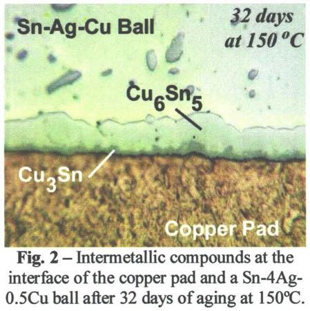
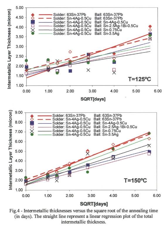
3 Table 1 Samples for the activation energy and the 4-point bending tests. The BGAs were removed from the motherboard using a handheld 'Dremel' cutting tool. A low speed diamond saw was used to cut through the component and expose the solder connections for metallographic preparation. The component segments were then potted in a low exotherm metallographic potting compound as to minimize the introduction of thermal artifacts on the solder microstructure. Once the sample was potted and marked with the appropriate identification, it was roughly ground to the proximity of the solder connections to be examined with an 80 grit abrasive belt. Further wet grinding on successively finer grit abrasive papers was carried out from 240 grit through 600 grit abrasives. Following the grinding, the samples were successively polished with 3 micron and then 1/4 micron diamond abrasives on a rotating polishing wheel covered with a synthetic polishing cloth. The final polishing step was then carried out on an automated vibratory polishing table using a 0.05-micron Alumina abrasive. The samples were then etched to more clearly reveal the reaction interfaces with the solder for the microscopic examination and the measurements of intermetallic layers thickness. Microscopic examination was carried out using a Zeiss Ultraphot II metallurgical microscope fitted with Optronics digital cameras and image capture software. Results and Discussion Figure 1 shows a general view of a lead-free solder joint. The Cu 6 Sn 5 intermetallic sublayer is clearly visible on each sample. The Cu 3 Sn sublayer is noticeable only for the sample annealed at 150 C. Figure 2 contains a micrograph of a lead-free ball aged at 150º C for 32 days. Comparison of the 63Sn-37Pb joints and the lead-free joints shows that the initial thickness of the intermetallic layer is not significantly impacted by the higher temperature used during the lead-free assembly process. All the values are in a range of 1.6 to 2.3 microns, as shown in Figure 3. The growth of these intermetallic layers can be modeled using parabolic growth kinetics [4]: w = w 0 + D t (1) Where: w = thickness of the intermetallic layer w 0 = initial thickness of the layer D = Diffusion coefficient t = time Figure 4 shows the intermetallic layer growth as a function of the square root of the annealing time. The straight lines represent a linear regression plot of the total intermetallic thickness (i.e. the combined thickness of the Cu 6 Sn 5 and Cu 3 Sn sublayers). These data indicate that the intermetallic layer growth is comparable from one sample to another. There are no significant differences in growth rate due to the paste metallurgy, the ball metallurgy or the peak temperature during the reflow process. Although these
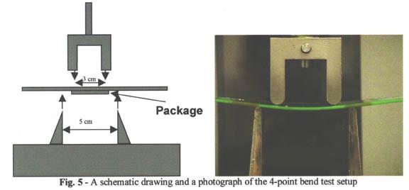
4 data are limited, it does not appear that intermetallic layer growth is faster for the leadfree joints than for the control Sn-Pb joints, and may in fact be somewhat slower. For each joint type, D was measured from the slopes in figure 4 at 32 days. The activation energy Q was measured assuming Arrhenius behavior, by plotting ln(d) versus 1/T. The results are reported in Table 2. Surface Mount BGA Solder Ball Activation Energy (kj/mol) Solder Paste Metallurgies 63Sn-37Pb 63Sn-37Pb 45 63Sn-37Pb 48 Sn-4.0Ag-0.5Cu 33 Sn-4.0Ag-0.5Cu Sn-2.5Ag-1.0Bi-0.5 Cu 68 Sn-0.75 Cu 50 Sn-3.5Ag 31 Table 2 Measured Activation energies for the solder joint type investigated. The value obtained for the Sn-Pb system (45 kj/mol) was found to be in accordance with the literature [5]. Qualitatively, it appears that the activation energies for the lead-free solders are within approximately +/- 50% of the value for 63Sn-37Pb. It also appears that the joints containing the highest amount of Ag (Sn-3.5Ag and Sn-4.0Ag-0.5Cu ) have the lowest activation energy. However, the scope of this study does not allow us to draw definite quantitative conclusions. The small number of test points and the design of the samples prevent us from doing so. In addition, we did not separate the contributions from the Cu 3 Sn and Cu 6 Sn 5 sublayers. Mechanical Strength As a preliminary investigation of the mechanical strength of Pb-free interconnects, fourpoint bending tests were performed to simulate the shipping and handling environment. Note that these tests were not meant to investigate the thermal fatigue or creep properties of the solder joints. Such investigations are underway and will be reported elsewhere. Experimental Procedure The test vehicle consisted of a 35mm x 35mm, daisy-chained 388 I/O PBGA package mounted on a 203 x 72 mm PCB. The four lead-free metallurgies described previously were used for the balls of the BGAs, and the Sn-4Ag-0.5Cu lead-free solder paste was used to attach the parts on the PCB. For control, BGAs with traditional 63Sn-37Pb solder balls were also assembled, with 63Sn-37Pb solder paste and with the Sn-4Ag-0.5Cu leadfree solder paste. In all cases OSP was used as the board finish. The assemblies were tested in 4-point bending on a screw-driven Instron testing machine (model # 5566). The crosshead speed was set to mm/min (0.03 in/min). Figure 5
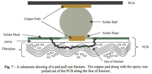
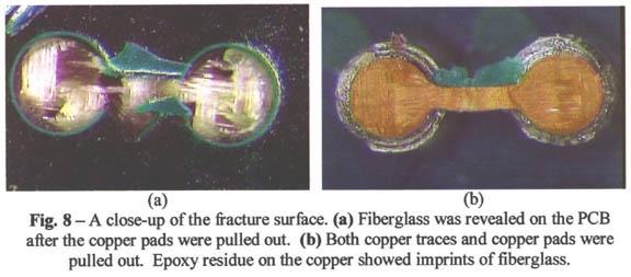
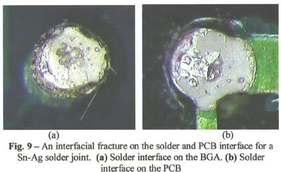
5 illustrates the experimental setup. A total of 4 samples per joint metallurgy (see Table 1) were tested. A multi-meter was used to monitor the continuity of electrical signals during the experiment. The BGA assemblies were tested to failure either discontinuity of electrical signal or separation of the BGA from the PCB. The experiments were run at room temperature. Results and Discussion A representative load vs. displacement plot for the 4-point bend test is shown in Figure 6. As a test assembly was loaded, the load vs. displacement plot followed a relatively straight line as both the PCB and BGA were bent. The load ultimately reached a maximum value, where the BGA separated from the board, and then decreased. The maximum load is defined as the fracture load. Table 3 lists the average fracture load for the Pb-free solder joints and the Sn-Pb control. Based on the results, the alloys can be broken into two groups. Joints containing Sn- 2.5Ag-1.0Bi-0.5Cu and Sn-3.5Ag alloys exhibited fracture loads in the range of 600N to 700N, similar to those with the eutectic 63Sn-37Pb. The second group, consisting of Sn- Ag-Cu and Sn-Cu, exhibited fracture loads ranging from 900N to 1050N. Standard deviations for the average fracture load of each alloy ranged from 27N-190N. Paste BGA Sample # Average Fracture Load (N) Standard Deviation Sn-Pb 63Sn-37Pb Sn-Ag-Cu 63Sn-37Pb Sn-4.0Ag-0.5Cu Sn-2.5Ag-1.0Bi-0.5 Cu Sn-0.75 Cu Sn-3.5Ag Table 3 Average and standard deviation of fracture load for Sn-Pb control and Pb-free Alloys All of the samples exhibited the same failure mode. The copper pads, along with some adjacent epoxy, were pulled out of the PCBs. Figure 7 provides a schematic drawing of this pad-pull-out failure mode. Figure 8(a) shows the fracture surface on the PCB side where the copper pads were pulled out, revealing the fiberglass underneath. Figure 8(b) is the mirror image on the BGA side. The copper traces and pads were pulled out of the PCB during the mechanical flexure test. Epoxy residue on the copper traces/pads showed imprints of the fiberglass that was underneath. In some rare cases, the corner solder joint exhibited an interfacial fracture or a pad-pullout fracture on the BGA package side. Interfacial fracture of a corner joint was observed for the Sn-0.75Cu and Sn-3.5Ag alloys. Figures 9 illustrates this failure mode. The pad-pull-out failure mode observed for the vast majority of samples indicates that the Pb-free solder joints are mechanically sound. Aside from the few cases of interfacial fractures along the corner solder joints, the solder joints were stronger than the epoxy holding the Cu pads to the PCB. Even in cases of interfacial fracture, the measured
6 fracture load was as high as that exhibited by the eutectic Sn-Pb control. Therefore, the interface between the solder and the BGA or PCB can withstand a substantial amount of stress. Since all but a few samples exhibited the pad-pull-out failure mode, one would expect similar fracture loads across the samples. However, the results showed two distinct groups of fracture load. Due to the small number of test samples and the large standard deviation within each group of alloy, a conclusive quantitative comparison of the mechanical strength of Pb-free solders and eutectic Sn-Pb solder cannot be drawn. Conclusions For the combinations of solder joint metallurgies studied, the following conclusions can be drawn: 1. The high temperature (250º C) reached during the lead-free assembly process does not lead to a significantly higher thickness of the intermetallic layer at the junction between the solder and the copper substrate. 2. After 32 days of annealing, the thicknesses of the intermetallic layers for the lead-free joints are slightly smaller than those for 63Sn-37Pb. 3. Four-point bend testing experiments showed that the lead-free joints are mechanically as sound as the joints made with 63Sn-37Pb. These combined results indicate that the higher assembly process temperature, the nature of the lead-free ball metallurgies and the lead-free solder paste are not a concern regarding the quantity and the brittleness of the intermetallics for the joint systems studied. Therefore, the reliability of these lead-free systems can be pursued with more extensive tests, such as accelerated thermal cycling. Acknowledgments The authors would like to acknowledge Jerry Ortkiese of HP and Fay Hua formerly with HP, now with Intel Corporation, for their continuous support and suggestions. REFERENCES [1] [2] S. Prasad, F. Carson, J.S. Lee, T.S. Jeong, Y.S. Kim, Reliability of Lead Free BGA Packages, Proceedings of IMAPS, Boston September 2000 [3] S. Prasad, F.Carson, G.S. Kim, J.S. Lee, P. Roubaud, G. Henshall, S. Kundar, A. Garcia, R. Herber, R. Bulwith., Board Level Reliability of Lead-Free Packages, Proceedings of SMTA, Chicago September 2000, pp
![[4] Wassink, R. J. Klein, Soldering in Electronics, 2 nd ed., 1989, Electrochemical Publications Li](/docs-images/76/73450312/images/7-0.jpg "mited, Ayr, Scotland. [5] P.T. Vianco, K.L.")
7 [4] Wassink, R. J. Klein, Soldering in Electronics, 2 nd ed., 1989, Electrochemical Publications Limited, Ayr, Scotland. [5] P.T. Vianco, K.L. Erickson, P.L. Hopkins, Solid State Intermetallic Compound Growth Between Copper and High Temperature, Tin-Rich Solders, Journal of Electronic Materials, Vol.23, No 8, 1994, p. 721
8

9
10
11
12
13
IMPACT OF COMPONENT TERMINAL FINISH ON THE RELIABILITY OF Pb-FREE SOLDER JOINTS
 IMPACT OF COMPONENT TERMINAL FINISH ON THE RELIABILITY OF Pb-FREE SOLDER JOINTS Gregory Henshall, Patrick Roubaud, Geary Chew Hewlett-Packard Co. Palo Alto, California greg_henshall@hp.com Swaminath Prasad,
Development of Baseline Lead-free Rework and Assembly Processes for Large Printed Circuit Assemblies
 Development of Baseline Lead-free Rework and Assembly Processes for Large Printed Circuit Assemblies Patrick Roubaud 1, Jerry Gleason 2, Charlie Reynolds, Ken Lyjak 4, Matt Kelly 5, Jasbir Bath 6 1 Hewlett
Low-Silver BGA Assembly Phase II Reliability Assessment Fifth Report: Preliminary Thermal Cycling Results
 Low-Silver BGA Assembly Phase II Reliability Assessment Fifth Report: Preliminary Thermal Cycling Results Gregory Henshall 1 Michael Fehrenbach 2 Hewlett-Packard Co. 1 Palo Alto, CA USA 2 Houston, TX USA
EFFECT OF Ag COMPOSITION, DWELL TIME AND COOLING RATE ON THE RELIABILITY OF Sn-Ag-Cu SOLDER JOINTS. Mulugeta Abtew
 EFFECT OF Ag COMPOSITION, DWELL TIME AND COOLING RATE ON THE RELIABILITY OF Sn-Ag-Cu SOLDER JOINTS Mulugeta Abtew Typical PCB Assembly Process PCB Loading Solder Paste Application Solder Paste Inspection
ENHANCING MECHANICAL SHOCK PERFORMANCE USING EDGEBOND TECHNOLOGY
 ENHANCING MECHANICAL SHOCK PERFORMANCE USING EDGEBOND TECHNOLOGY Steven Perng, Tae-Kyu Lee, and Cherif Guirguis Cisco Systems, Inc. San Jose, CA, USA sperng@cisco.com Edward S. Ibe Zymet, Inc. East Hanover,
Reliability of Lead-Free Solder Connections for Area-Array Packages
 Presented at IPC SMEMA Council APEX SM 2001 For additional information, please email marketing@amkor.com Reliability of Lead-Free Solder Connections for Area-Array Packages Ahmer Syed Amkor Technology,
Manufacturability and Reliability Impacts of Alternate Pb-Free BGA Ball Alloys. June 2007
 Manufacturability and Reliability Impacts of Alternate Pb-Free BGA Ball Alloys Greg Henshall Michael Roesch Kris Troxel Helen Holder Jian Miremadi HP Global Engineering Services The information contained
Growth Kinetics of Reaction Layers in Flip Chip Joints with Cu-cored Lead-free Solder Balls
 Materials Transactions, Vol. 5, No. 3 () pp. 75 to 75 Special Issue on Lead-Free Soldering in Electronics # The Japan Institute of Metals Growth Kinetics of Reaction Layers in Flip Chip Joints with Cu-cored
Composition/wt% Bal SA2 (SABI) Bal SA3 (SABI + Cu) Bal
 Bal SA3 (SABI + Cu) Bal") Improving Thermal Cycle and Mechanical Drop Impact Resistance of a Lead-free Tin-Silver-Bismuth-Indium Solder Alloy with Minor Doping of Copper Additive Takehiro Wada 1, Seiji Tsuchiya 1, Shantanu Joshi
Improving Thermal Cycle and Mechanical Drop Impact Resistance of a Lead-free Tin-Silver-Bismuth-Indium Solder Alloy with Minor Doping of Copper Additive Takehiro Wada 1, Seiji Tsuchiya 1, Shantanu Joshi
Comparison of Thermal Fatigue Performance of SAC105 (Sn-1.0Ag-0.5Cu), Sn- 3.5Ag, and SAC305 (Sn-3.0Ag-0.5Cu) BGA Components with SAC305 Solder Paste
, Sn- 3.5Ag, and SAC305 (Sn-3.0Ag-0.5Cu) BGA Components with SAC305 Solder Paste") Comparison of Thermal Fatigue Performance of SAC105 (Sn-1.0Ag-0.5Cu), Sn- 3.5Ag, and SAC305 (Sn-3.0Ag-0.5Cu) BGA Components with SAC305 Solder Paste Gregory Henshall, Hewlett-Packard Co. Palo Alto, CA
Comparison of Thermal Fatigue Performance of SAC105 (Sn-1.0Ag-0.5Cu), Sn- 3.5Ag, and SAC305 (Sn-3.0Ag-0.5Cu) BGA Components with SAC305 Solder Paste Gregory Henshall, Hewlett-Packard Co. Palo Alto, CA
Welcome to SMTA Brazil Chapter Brook Sandy-Smith Dr. Ron Lasky Tim Jensen
 Welcome to SMTA Brazil Chapter 2013 Presented by Authors Ivan Castellanos Edward Briggs Brook Sandy-Smith Dr. Ron Lasky Tim Jensen Advantages / Concerns HP testing Mechanical properties New work Area ratio
Study of the Interface Microstructure of Sn-Ag-Cu Lead-Free Solders and the Effect of Solder Volume on Intermetallic Layer Formation.
 Study of the Interface Microstructure of Sn-Ag-Cu Lead-Free Solders and the Effect of Solder Volume on Intermetallic Layer Formation. B. Salam +, N. N. Ekere, D. Rajkumar Electronics Manufacturing Engineering
LOW-SILVER BGA ASSEMBLY PHASE I REFLOW CONSIDERATIONS AND JOINT HOMOGENEITY SECOND REPORT: SAC105 SPHERES WITH TIN-LEAD PASTE
 LOW-SILVER BGA ASSEMBLY PHASE I REFLOW CONSIDERATIONS AND JOINT HOMOGENEITY SECOND REPORT: SAC105 SPHERES WITH TIN-LEAD PASTE Chrys Shea Ranjit Pandher Cookson Electronics South Plainfield, NJ, USA Ken
RELIABILITY OF DOPED LEAD-FREE SOLDER JOINTS UNDER ISOTHERMAL AGING AND THERMAL CYCLING
 As originally published in the SMTA Proceedings RELIABILITY OF DOPED LEAD-FREE SOLDER JOINTS UNDER ISOTHERMAL AGING AND THERMAL CYCLING Cong Zhao, Thomas Sanders, Chaobo Shen, Zhou Hai, John L. Evans,
Reflow profile study of the Sn-Ag-Cu solder
 B. Salam School of Engineering, University of Greenwich, Kent, UK C. Virseda European Fuel Cell H. Da School of Engineering, University of Greenwich, Kent, UK N.N. Ekere School of Engineering, University
Acceptance Testing Of Low-Ag Reflow Solder Alloys
 Acceptance Testing Of Low-Ag Reflow Solder Alloys Kris Troxel 1, Aileen Allen 2, Elizabeth Elias Benedetto 3, Rahul Joshi 3 Hewlett-Packard Company 1 Boise, ID, USA 2 Palo Alto, CA, USA 3 Houston, TX,
THE EFFECTS OF PLATING MATERIALS, BOND PAD SIZE AND BOND PAD GEOMETRY ON SOLDER BALL SHEAR STRENGTH
 THE EFFECTS OF PLATING MATERIALS, BOND PAD SIZE AND BOND PAD GEOMETRY ON SOLDER BALL SHEAR STRENGTH Keith Rogers and Craig Hillman CALCE Electronic Products and Systems Center University of Maryland College
Sn-RICH PHASE COARSENING DURING ISOTHERMAL ANNEALING ON Sn-Ag-Cu SOLDER. N. Saud and A. Jalar
 International Journal of Mechanical and Materials Engineering (IJMME), Vol. 4 (2009), No. 2, 147-151 Sn-RICH PHASE COARSENING DURING ISOTHERMAL ANNEALING ON Sn-Ag-Cu SOLDER. N. Saud and A. Jalar School
Investigation of Pad Cratering in Large Flip-Chip BGA using Acoustic Emission
 Investigation of Pad Cratering in Large Flip-Chip BGA using Acoustic Emission Anurag Bansal, Cherif Guirguis and Kuo-Chuan Liu Cisco Systems, Inc., San Jose, CA anurbans@cisco.com Abstract Electronics
HOW THE MOLD COMPOUND THERMAL EXPANSION OVERRULES THE SOLDER COMPOSITION CHOICE IN BOARD LEVEL RELIABILITY PERFORMANCE
 HOW THE MOLD COMPOUND THERMAL EXPANSION OVERRULES THE SOLDER COMPOSITION CHOICE IN BOARD LEVEL RELIABILITY PERFORMANCE AUTHORS: B. VANDEVELDE, L. DEGRENDELE, M. CAUWE, B. ALLAERT, R. LAUWAERT, G. WILLEMS
New Pb-Free Solder Alloy for Demanding Applications. Presented by Karl Seelig, VP Technology, AIM
 New Pb-Free Solder Alloy for Demanding Applications Presented by Karl Seelig, VP Technology, AIM Why REL? The evolution and expansion of electronics into more harsh operating environments performing more
Evaluation of Pb-free BGA Solder Joint Reliability on Ni-based Surface Finishes using Alternative Shear and Pull Metrologies
 Evaluation of Pb-free BGA Solder Joint Reliability on Ni-based Surface Finishes using Alternative Shear and Pull Metrologies Kuldip Johal and Hugh Roberts Atotech USA Inc., Rock Hill, SC Sven Lamprecht,
Effect of Process Variations on Solder Joint Reliability for Nickel-based Surface Finishes
 Effect of Process Variations on Solder Joint Reliability for Nickel-based Surface Finishes Hugh Roberts Atotech USA Inc., Rock Hill, SC, USA Sven Lamprecht, Gustavo Ramos and Christian Sebald Atotech Deutschland
Component Palladium Lead Finish - Specification Approved by Executive Board 1997-xx-xx August 22 Version
 Component Palladium Lead Finish - Specification Approved by Executive Board 1997-xx-xx August 22 Version Appendices 1. User Commitment Form 2. Supplier Compliance Form Table of contents 1. Background 2.
EFFECT OF SOLDER COMPOSITION, PCB SURFACE FINISH AND SOLDER JOINT VOLUME ON DROP SHOCK RELIABILITY
 As originally published in the SMTA Proceedings EFFECT OF SOLDER COMPOSITION, PCB SURFACE FINISH AND SOLDER JOINT VOLUME ON DROP SHOCK RELIABILITY Shuai Shao 1, Francis Mutuku 1,2, Babak Arfaei, Ph.D.
Impact of External Temperature Environment on Large FCBGA Sn-Ag-Cu Solder Interconnect Board Level Mechanical Shock Performance
 Impact of External Temperature Environment on Large FCBGA Sn-Ag-Cu Solder Interconnect Board Level Mechanical Shock Performance Tae-Kyu Lee Journal of Welding and Joining(Vol. 32, No. 3) 2014. 6 53 Research
Lead-Contamination in Lead-Free Electronics Assembly Karl Seelig and David Suraski AIM
 Lead-Contamination in Lead-Free Electronics Assembly Karl Seelig and David Suraski AIM The question of what happens to a lead-free solder joint if it becomes contaminated with lead is important because
A New Approach for Early Detection of PCB Pad Cratering Failures
 A New Approach for Early Detection of PCB Pad Cratering Failures Anurag Bansal, Gnyaneshwar Ramakrishna and Kuo-Chuan Liu Cisco Systems, Inc., San Jose, CA anurbans@cisco.com Abstract Pad cratering refers
DEVELOPMENT OF LEAD-FREE ALLOYS WITH ULTRA-HIGH THERMO- MECHANICAL RELIABILITY
 As originally published in the SMTA Proceedings. DEVELOPMENT OF LEAD-FREE ALLOYS WITH ULTRA-HIGH THERMO- MECHANICAL RELIABILITY Pritha Choudhury, Ph.D., Morgana Ribas, Ph.D., Ranjit Pandher, Ph.D., Anil
Unique Failure Modes from use of Sn-Pb and Lead-Free (mixed metallurgies) in PCB Assembly: CASE STUDY
 in PCB Assembly: CASE STUDY") Unique Failure Modes from use of Sn-Pb and Lead-Free (mixed metallurgies) in PCB Assembly: CASE STUDY Frank Toth, and Gary F. Shade; Intel Corporation, Hillsboro, OR, USA {francis.toth.jr@intel.com, (503)-696-1546}
Unique Failure Modes from use of Sn-Pb and Lead-Free (mixed metallurgies) in PCB Assembly: CASE STUDY Frank Toth, and Gary F. Shade; Intel Corporation, Hillsboro, OR, USA {francis.toth.jr@intel.com, (503)-696-1546}
Best Practice Guide for Thermocycling and Reliability Assessment of Solder Joints
 Best Practice Guide for Thermocycling and Reliability Assessment of Solder Joints Miloš Dušek and Christopher Hunt July 2000 July 2000 Best Practice Guide for Thermocycling and Reliability Assessment of
Investigation of the recommended immersion Tin thickness for Pbfree
 Investigation of the recommended immersion Tin thickness for Pbfree soldering Sven Lamprecht Atotech Deutschland GmbH Berlin Abstract First choices for Pb-free soldering are SnAgCu alloys, which are in
ENHANCING WLCSP RELIABILITY THROUGH BUILD-UP STRUCTURE IMPROVEMENTS AND NEW SOLDER ALLOYS
 ENHANCING WLCSP RELIABILITY THROUGH BUILD-UP STRUCTURE IMPROVEMENTS AND NEW SOLDER ALLOYS B. Rogers, M. Melgo, M. Almonte, S. Jayaraman, C. Scanlan, and T. Olson Deca Technologies, Inc 7855 S. River Parkway,
Creep Rates and Stress Relaxation for Micro-sized Lead-free Solder Joints
 Creep Rates and Stress Relaxation for Micro-sized Lead-free Solder Joints Summary This Note describes a new method for the measurement of some materials properties of lead-free solders, in particular the
Board Level Reliability of BGA Multichip Modules
 Board Level Reliability of BGA Multichip Modules Robert Darveaux and Bhuvaneshwaran Vijayakumar Skyworks Solutions, Inc. Irvine, CA robert.darveaux@skyworksinc.com ABSTRACT The board level reliability
Thermal Fatigue Result for Low and No-Ag Alloys - Pb-Free Alloy Characterization Speaker: William Chao, Cisco Chair: Elizabeth Benedetto, HP
 Thermal Fatigue Result for Low and No-Ag Alloys - Pb-Free Alloy Characterization Speaker: William Chao, Cisco Chair: Elizabeth Benedetto, HP October 26, 2012 inemi Session, IMPACT Project Team Members
Effects of Thermal Aging on Copper Dissolution For SAC 405 Alloy
 Effects of Thermal Aging on Copper Dissolution For SAC 405 Alloy Dr. Dana Medlin, Clay Voyles, Teneil Ryno, Casey Bergstrom, John Metzger, and Spencer Richards Abstract: Aging characteristics of new lead
Composition/wt% Bal SA2 (SABI) Bal SA3 (SABI + Cu) Bal
 Bal SA3 (SABI + Cu) Bal") Improving Thermal Cycle and Mechanical Drop Impact Resistance of a Lead-free Tin-Silver-Bismuth-Indium Solder Alloy with Minor Doping of Copper Additive Takehiro Wada 1, Seiji Tsuchiya 1, Shantanu Joshi
Improving Thermal Cycle and Mechanical Drop Impact Resistance of a Lead-free Tin-Silver-Bismuth-Indium Solder Alloy with Minor Doping of Copper Additive Takehiro Wada 1, Seiji Tsuchiya 1, Shantanu Joshi
Ball shear strength and fracture mode of lead-free solder joints prepared using nickel nanoparticle doped flux
 Ball shear strength and fracture mode of lead-free solder joints prepared using nickel nanoparticle doped flux G. K. Sujan a, A. S. M. A. Haseeb a, *, Chong Hoe Jian b, Amalina Afifi a a Department of
System Level Effects on Solder Joint Reliability
 System Level Effects on Solder Joint Reliability Maxim Serebreni 2004 2010 Outline Thermo-mechanical Fatigue of solder interconnects Shear and tensile effects on Solder Fatigue Effect of Glass Style on
Validated Test Method to Characterize and Quantify Pad Cratering Under Bga Pads on Printed Circuit Boards
 Validated Test Method to Characterize and Quantify Pad Cratering Under Bga Pads on Printed Circuit Boards Mudasir Ahmad, Jennifer Burlingame, Cherif Guirguis Technology and Quality Group Cisco Systems,
The Morphology Evolution and Voiding of Solder Joints on QFN Central Pads with a Ni/Au Finish
 The Morphology Evolution and Voiding of Solder Joints on QFN Central Pads with a Ni/Au Finish Julie Silk 1, Jianbiao Pan 2, Mike Powers 1 1 Agilent Technologies, 1400 Fountaingrove Parkway, Santa Rosa,
Forward and Backward Soldering Compatibility
 Forward and Backward Soldering Compatibility You are connected to our live presentation delivered via the internet. The webinar will begin shortly. NEW 1 Attendee Quick Reference You can ask questions
Thermal Cycling Reliability Screening of Multiple Pb-free Solder Ball Alloys
 Thermal Cycling Reliability Screening of Multiple Pb-free Solder Ball Alloys Joe Smetana 1, Richard Coyle 1, and Peter Read 1 Thomas Koshmeider 2, Dave Love 3, Mark Kolenik 4, and Jennifer Nguyen 5 1 Alcatel-Lucent,
Freescale Semiconductor Tape Ball Grid Array (TBGA) Overview
 Overview") Freescale Semiconductor Tape Ball Grid Array (TBGA) Overview Revision 0 2006 Freescale and the Freescale logo are trademarks of Freescale Semiconductor, Inc. All other product or service names are the
Freescale Semiconductor Tape Ball Grid Array (TBGA) Overview Revision 0 2006 Freescale and the Freescale logo are trademarks of Freescale Semiconductor, Inc. All other product or service names are the
BOARD LEVEL RELIABILITY COMPARISON OF LEAD FREE ALLOYS
 BOARD LEVEL RELIABILITY COMPARISON OF LEAD FREE ALLOYS Robert Darveaux, Corey Reichman, Sabira Enayet, Wen-Sung Hsu, and Win Thandar Swe Amkor Technology, Inc. Chandler, AZ, USA rdarv@amkor.com ABSTRACT
Freescale, the Freescale logo, AltiVec, C-5, CodeTEST, CodeWarrior, ColdFire, C-Ware, t he Energy Efficient Solutions logo, mobilegt, PowerQUICC,
 TM February 2012 Freescale, the Freescale logo, AltiVec, C-5, CodeTEST, CodeWarrior, ColdFire, C-Ware, t he Energy Efficient Solutions logo, mobilegt, PowerQUICC, QorIQ, StarCore and Symphony are trademarks
MICROSTRUCTURE AND RELIABILITY OF LOW AG, BI-CONTAINING SOLDER ALLOYS
 MICROSTRUCTURE AND RELIABILITY OF LOW AG, BI-CONTAINING SOLDER ALLOYS Eva Kosiba, Simin Bagheri, Polina Snugovsky, Ph.D. Celestica Inc. Toronto, ON, Canada ekosiba@celestica.com, sbagheri@celestica.com,
Simulations and Characterizations for Stress Reduction Designs in Wafer Level Chip Scale Packages
 Simulations and Characterizations for Stress Reduction Designs in Wafer Level Chip Scale Packages by Ming-Che Hsieh STATS ChipPAC Taiwan Co. Ltd. Copyright 2013. Reprinted from 2013 International Microsystems,
The Effect of Cu and Ni on the Structure and Properties of the IMC Formed by the Reaction of Liquid Sn-Cu Based Solders with Cu Substrate
 WDS'08 Proceedings of Contributed Papers, Part III, 220 224, 2008. ISBN 978-80-7378-067-8 MATFYZPRESS The Effect of Cu and Ni on the Structure and Properties of the IMC Formed by the Reaction of Liquid
Interfacial Reactions between the Sn-9Zn Solder and Au/Ni/SUS304 Multi-layer Substrate
 , July 6-8, 2011, London, U.K. Interfacial Reactions between the Sn-9Zn Solder and Au/Ni/SUS304 Multi-layer Substrate *Yee-Wen Yen 1, Chien-Chung Jao 2, Kuo-Sing Chao 1, Shu-Mei Fu Abstract Sn-9Zn lead-free
room and cold readouts were performed every 250 cycles. Failure data and Weibull plots were generated. Typically, the test vehicles were subjected to
 SOLDER JOINT RELIABILITY ASSESMENT OF Sn-Ag-Cu BGA COMPONENTS ATTACHED WITH EUTECTIC Pb-Sn SOLDER Fay Hua 1, Raiyo Aspandiar 2, Cameron Anderson 3, Greg Clemons 3, Chee-key Chung 4, Mustapha Faizul 4 Intel
Flip Chip Bump Electromigration Reliability: A comparison of Cu Pillar, High Pb, SnAg, and SnPb Bump Structures
 Flip Chip Bump Electromigration Reliability: A comparison of Cu Pillar,,, and SnPb Bump Structures Ahmer Syed, Karthikeyan Dhandapani, Lou Nicholls, Robert Moody, CJ Berry, and Robert Darveaux Amkor Technology
Reflow Profiling: Time a bove Liquidus
 Reflow Profiling: Time a bove Liquidus AIM/David Suraski Despite much research and discussion on the subject of reflow profiling, many questions and a good deal of confusion still exist. What is clear
THE EFFECTS OF INTERNAL STRESSRS IN BGA Ni LAYER ON THE STRENGTH OF Sn/Ag/Cu SOLDER JOINT
 THE EFFECTS OF INTERNAL STRESSRS IN BGA Ni LAYER ON THE STRENGTH OF Sn/Ag/Cu SOLDER JOINT C.H. Chien 1, * C.J. Tseng 1,2 T.P. Chen 1,3 1 Department of Mechanical and Electro-Mechanical Engineering, National
SCV Chapter, CPMT Society, IEEE September 14, Voids at Cu / Solder Interface and Their Effects on Solder Joint Reliability
 Voids at / Solder Interface and Their Effects on Solder Joint Reliability Zequn Mei, Mudasir Ahmad, Mason Hu, Gnyaneshwar Ramakrishna Manufacturing Technology Group Cisco Systems, Inc. Acknowledgement:
Evaluation of Stripped and Replated Component Termination Finishes
 Evaluation of Stripped and Replated Component Termination Finishes Guhan Subbarayan, Robert Kinyanjui Sanmina-SCI Michael Baker E-Certa ABSTRACT In this study, the termination finish of Small Output Integrated
Aging Studies of PBGA Solder Joints Reflowed at Different Conveyor Speeds
 Aging Studies of PBGA Solder Joints Reflowed at Different Conveyor Speeds S. H.,Fan*, Y. C. Chant, C. W. Tang and J. K. L. La? Department of Electronic Engineering and Department of Physics and Materials
The mechanical properties and microstructures of copper and brass joints soldered with eutectic tin-bismuth solder
 JOURNAL OF MATERIALS SCIENCE 22 (1987) 1835-1839 The mechanical properties and microstructures of copper and brass joints soldered with eutectic tin-bismuth solder W. J. TOMLINSON, I. COLLIER Department
EFFECT OF THERMAL AGING ON THE IMC LAYER BETWEEN SnAgSb SOLDER AND Cu SUBSTRATE. Universiti Kebangsaan Malaysia, 43600, Bangi, Selangor, Malaysia
 EFFECT OF THERMAL AGING ON THE IMC LAYER BETWEEN SnAgSb SOLDER AND Cu SUBSTRATE W. Shualdi 1, I. Ahmad 1, G. Omar 2 and A. Isnin 3 1 Department of Electrical, Electronic and System, Faculty of Engineering,
Traditional Solder Materials
 Traditional Solder Materials Characteristics of tin-lead solders In Metal basics we showed how cooling curves are used to produce a composite thermal equilibrium (or phase ) diagram of the tin-lead system.
Future Electronic Devices Technology in Cosmic Space and Lead-free Solder Joint Reliability
 The 22nd Microelectronics Work Future Electronic Devices Technology in Cosmic Space and Lead-free Solder Joint Reliability Key Points (1) High Speed Solder Ball Shear Test (2) Relationship between Surface
Thermal cyclic test for Sn-4Ag-0.5Cu solders on high P Ni/Au and Ni/Pd/Au surface finishes
 Journal of Mechanical Engineering and Sciences (JMES) ISSN (Print): 2289-4659; e-issn: 2231-8380; Volume 9, pp. 1572-1579, December 2015 Universiti Malaysia Pahang, Malaysia DOI: http://dx.doi.org/10.15282/jmes.9.2015.4.0152
Solder joint reliability of plastic ball grid array with solder bumped flip chip
 ball grid array with solder bumped Shi-Wei Ricky Lee Department of Mechanical Engineering, The Hong Kong University of Science and, Kowloon, Hong Kong John H. Lau Express Packaging Systems, Inc., Palo
Qualification of Thin Form Factor PWBs for Handset Assembly
 Qualification of Thin Form Factor PWBs for Handset Assembly Mumtaz Y. Bora Kyocera Wireless Corporation San Diego, Ca. 92121 mbora@kyocera-wreless.com Abstract: The handheld wireless product market place
PROCESSING AND RELIABILITY OF LOW-SILVER-ALLOYS
 PROCESSING AND RELIABILITY OF LOW-SILVER-ALLOYS Mathias Nowottnick and Andrej Novikov University of Rostock Rostock, Germany mathias.nowottnick@uni-rostock.de Joerg Trodler W.C. Heraeus Hanau, Germany
Effect of Ni and Ag on Interfacial Reaction and Microstructure of Sn-Ag-Cu-Ni-Ge Lead-Free Solder
 Reprinted with permission of Materials Science & Technology 2006 Conference and Exhibition Proceedings Effect of Ni and Ag on Interfacial Reaction and Microstructure of Sn-Ag-Cu-Ni-Ge Lead-Free Solder
SOLDER-JOINT RELIABILITY OF 0.8MM BGA PACKAGES FOR AUTOMOTIVE APPLICATIONS
 As originally published in the SMTA Proceedings. SOLDER-JOINT RELIABILITY OF 0.8MM BGA PACKAGES FOR AUTOMOTIVE APPLICATIONS Burton Carpenter Freescale Semiconductor, Inc. Austin, TX, USA Burt.Carpenter@freescale.com
Reliability of Pb-Free Solder Alloys in Demanding BGA and CSP Applications
 Reliability of Pb-Free Solder Alloys in Demanding BGA and CSP Applications Ranjit Pandher and Robert Healey Cookson Electronics 109 Corporate Blvd. South Plainfield, NJ 07080, USA Email: rpandher@cooksonelectronics.com
Intermetallic Reactions in a Sn-20In-2.8Ag Solder Ball-Grid-Array Package with Au/Ni/Cu Pads
 Journal of ELECTRONIC MATERIALS, Vol. 34, No. 11, 2005 Regular Issue Paper Intermetallic Reactions in a Sn-20In-2.8Ag Solder Ball-Grid-Array Package with Au/Ni/Cu Pads HUI-MIN WU, 1,2 FENG-CHIH WU, 1 and
A study aimed at characterizing the interfacial structure in a tin silver solder on nickel-coated copper plate during aging
 Sādhanā Vol. 33, Part 3, June 2008, pp. 251 259. Printed in India A study aimed at characterizing the interfacial structure in a tin silver solder on nickel-coated copper plate during aging D C LIN 1,
Solder Alloy Evolution and Development
 Solder Alloy Evolution and Development SMTA Boston November 4, 2018 Presented by Timothy O Neill, Technical Marketing Manager, AIM A Brief Review of Electronic Solders 1960 s to 2006 Tin/Lead (Sn/Pb) Solder
Growth of Intermetallic Compounds during Isothermal Annealing of a Sn-Ag-Cu Lead-free Solder
 Accepted for publication in Soldering & Surface Mount Technology, Emerald, United Kingdom, 2004, in press. Growth of Intermetallic Compounds during Isothermal Annealing of a Sn-Ag-Cu Lead-free Solder S.L.
TMS320C6x Manufacturing with the BGA Package
 TMS320C6x Manufacturing with the BGA Package APPLICATION REPORT: SPRA429 David Bell Digital Signal Processing Solutions March 1998 IMPORTANT NOTICE Texas Instruments (TI) reserves the right to make changes
Solder Joint Reliability Study for Plastic Ball Grid Array Packages
 Intl. Journal of Microcircuits and Electronic Packaging Solder Joint Reliability Study for Plastic Ball Grid Array Packages L. Y. Yang and Y. C. Mui Advanced Packaging Advanced Micro Devices (AMD) 512
ANALYSIS OF RING AND PLUG SHEAR STRENGTHS FOR COMPARISON OF LEAD FREE SOLDERS
 ANALYSIS OF RING AND PLUG SHEAR STRENGTHS FOR COMPARISON OF LEAD FREE SOLDERS J.C. Foley, A. Gickler, F.H. LePrevost, and D. Brown Ames Laboratory, 122 Metals Development, Ames, IA 50011, Johnson Manufacturing
Intermetallic Compounds Formed in Sn-20In-2.8Ag Solder BGA Packages with Ag/Cu Pads C.C. Jain, S.S. Wang, K.W. Huang, and T.H.
 JMEPEG ÓASM International DOI: 10.1007/s11665-008-9292-7 1059-9495/$19.00 Intermetallic Compounds Formed in Sn-20In-2.8Ag Solder BGA Packages with Ag/Cu Pads C.C. Jain, S.S. Wang, K.W. Huang, and T.H.
Via Life vs. Temperature Stress Analysis of Interconnect Stress Test
 Page 1 of 12 N P All BNP Media LINX Search H i 3 w Want to use this article? CLICK HERE for options!
Thermo-Mechanical FEM Analysis of Lead Free and Lead Containing Solder for Flip Chip Applications
 Thermo-Mechanical FEM Analysis of Lead Free and Lead Containing Solder for Flip Chip Applications M. Gonzalez 1, B. Vandevelde 1, Jan Vanfleteren 2 and D. Manessis 3 1 IMEC, Kapeldreef 75, 3001, Leuven,
Optimizing Immersion Silver Chemistries For Copper
 Optimizing Immersion Silver Chemistries For Copper Ms Dagmara Charyk, Mr. Tom Tyson, Mr. Eric Stafstrom, Dr. Ron Morrissey, Technic Inc Cranston RI Abstract: Immersion silver chemistry has been promoted
EXTRA FINE PITCH FLIP CHIP ASSEMBLY PROCESS, UNDERFILL EVALUATION AND RELIABILITY
 As originally published in the SMTA Proceedings EXTRA FINE PITCH FLIP CHIP ASSEMBLY PROCESS, UNDERFILL EVALUATION AND RELIABILITY Fei Xie, Ph.D. *, Daniel F. Baldwin, Ph.D. *, Han Wu *, Swapon Bhattacharya,
Yasunori Chonan 1,2,, Takao Komiyama 1, Jin Onuki 1, Ryoichi Urao 2, Takashi Kimura 3 and Takahiro Nagano Introduction
 Materials Transactions, Vol. 43, No. 8 (2002) pp. 1840 to 1846 Special Issue on Lead-Free Electronics Packaging c 2002 The Japan Institute of Metals Influence of Phosphorus Concentration in Electroless
contaminated, or if the location of the assembly house is well above sea level.
 VAPOR PHASE REFLOW S EFFECT ON SOLDER PASTE RESIDUE SURFACE INSULATION RESISTANCE Karen Tellefsen. Mitch Holtzer, Corne Hoppenbrouwers Alpha Assembly Solutions South Plainfield, NJ, USA Roald Gontrum SmartTech
Characterization of Coined Solder Bumps on PCB Pads
 Characterization of Coined Solder Bumps on PCB Pads Jae-Woong Nah, Kyung W. Paik, Won-Hoe Kim*, and Ki-Rok Hur** Department of Materials Sci. & Eng., Korea Advanced Institute of Science and Technology
2006 DMSMS Conference Pb-free Solder Technical Issues (Not Including Tin Whiskers)
") 2006 DMSMS Conference Pb-free Solder Technical Issues (Not Including Tin Whiskers) Dr. Stephan Meschter BAE Systems LEAP WG Technical Guidelines Handbook Leader Johnson City, NY Phone: 607-770-2332, Email:
2006 DMSMS Conference Pb-free Solder Technical Issues (Not Including Tin Whiskers) Dr. Stephan Meschter BAE Systems LEAP WG Technical Guidelines Handbook Leader Johnson City, NY Phone: 607-770-2332, Email:
Building HDI Structures using Thin Films and Low Temperature Sintering Paste
 Building HDI Structures using Thin Films and Low Temperature Sintering Paste Catherine Shearer, James Haley and Chris Hunrath Ormet Circuits Inc. - Integral Technology California, USA chunrath@integral-hdi.com
Lead-Free HASL: Balancing Benefits and Risks for IBM Server and Storage Hardware
 Lead-Free HASL: Balancing Benefits and Risks for IBM Server and Storage Hardware November 19, 2009 M.Kelly, P.Eng, MBA Senior Engineer, ECAT Interconnect Technology Lead-Free Server Development Core Team
COMPONENT LEVEL RELIABILITY FOR HIGH TEMPERATURE POWER COMPUTING WITH SAC305 AND ALTERNATIVE HIGH RELIABILITY SOLDERS
 As originally published in the SMTA Proceedings. COMPONENT LEVEL RELIABILITY FOR HIGH TEMPERATURE POWER COMPUTING WITH SAC305 AND ALTERNATIVE HIGH RELIABILITY SOLDERS Thomas Sanders, Sivasubramanian Thirugnanasambandam
Solder joint reliability of cavity-down plastic ball grid array assemblies
 cavity-down plastic ball grid array S.-W. Ricky Lee Department of Mechanical Engineering, The Hong Kong University of Science and, Kowloon, Hong Kong John H. Lau Express Packaging Systems, Inc., Palo Alto,
Reliability Testing of Ni-Modified SnCu and SAC305 - Vibration. Keith Sweatman, Nihon Superior Joelle Arnold, DfR Solutions March 2008
 Reliability Testing of Ni-Modified SnCu and SAC305 - Vibration Keith Sweatman, Nihon Superior Joelle Arnold, DfR Solutions March 2008 2004-2008 Previous Work Accelerated Life Testing of SN100C for Surface
A STUDY ON PROCESS, STRENGTH AND MICROSTRUCTURE ANALYSIS OF LOW TEMPERATURE SnBi CONTAINING SOLDER PASTES MIXED WITH LEAD-FREE SOLDER BALLS
 As originally published in the SMTA Proceedings A STUDY ON PROCESS, STRENGTH AND MICROSTRUCTURE ANALYSIS OF LOW TEMPERATURE SnBi CONTAINING SOLDER PASTES MIXED WITH LEAD-FREE SOLDER BALLS Sakthi Cibi Kannammal
Effect of Alloying Element on Microstructure and Mechanical Properties of Sn-0.7cu Solder
 International Journal of Current Science, Engineering & Technology Original Research Article Open Access AMCT 2017 Malaysia Special Issue ISSN : 2581-4311 Effect of Alloying Element on Microstructure and
Effects of Minor Fe, Co, and Ni Additions on the Reaction Between SnAgCu Solder and Cu
 Effects of Minor Fe, Co, and Ni Additions on the Reaction Between SnAgCu Solder and Cu Y. W. Wang, C. R. Kao* Department of Materials Science and Engineering National Taiwan University Taipei 106, Taiwan
Brittle Failure Mechanism of SnAgCu and SnPb Solder Balls during High Speed Ball Shear and Cold Ball Pull Tests
 Brittle Failure Mechanism of SnAgCu and SnPb Solder Balls during High Speed Ball Shear and Cold Ball Pull Tests Fubin Song 1, S. W. Ricky Lee 1, Keith Newman 2, Bob Sykes 3, Stephen Clark 3 1 EPACK Lab,
Effect of local grain distribution and Enhancement on edgebond applied wafer-level chip-scale package (WLCSP) thermal cycling performance
 thermal cycling performance") Effect of local grain distribution and Enhancement on edgebond applied wafer-level chip-scale package (WLCSP) thermal cycling performance 1 Tae-Kyu Lee, 2 Weidong Xie, 2 Steven Perng, 3 Edward Ibe, and
Effect of local grain distribution and Enhancement on edgebond applied wafer-level chip-scale package (WLCSP) thermal cycling performance 1 Tae-Kyu Lee, 2 Weidong Xie, 2 Steven Perng, 3 Edward Ibe, and
Design for Plastic Ball Grid Array Solder Joint Reliability. S.-W. R. Lee, J. H. Lau*
 Page 1 of 9 Design for Plastic Ball Grid Array Solder Joint Reliability The Authors S.-W. R. Lee, J. H. Lau* S.-W. R. Lee, Department of Mechanical Engineering, The Hong Kong University of Science and
ALT of Lead Free CCAs
 ALT of Lead Free CCAs OPS Value Propositions Ops A La Carte is a Professional Reliability Engineering firm focused on providing confidence in reliability. Flexible method of engagement from end to end
Interfacial Reactions of Ni-doped SAC105 and SAC405 Solders on Ni-Au Finish during Multiple Reflows
 Interfacial Reactions of Ni-doped SAC105 and Solders on Ni-Au Finish during Multiple Reflows Toh C.H. 1, Liu Hao 1, Tu C.T 2., Chen T.D. 2, and Jessica Yeo 1 1 United Test and Assembly Center Ltd, 5 Serangoon
Lead-Free Solder Bump Technologies for Flip-Chip Packaging Applications
 Lead-Free Solder Bump Technologies for Flip-Chip Packaging Applications Zaheed S. Karim 1 and Jim Martin 2 1 Advanced Interconnect Technology Ltd. 1901 Sunley Centre, 9 Wing Yin Street, Tsuen Wan, Hong
The No Lead manufacturing Initiative
 The No Lead manufacturing Initiative Dr. Srinivas T. Rao UCLA Workshop on Lead-free Solder for Electronic, Optical, and MEMs Packaging and Manufacturing September 5 th 2002 Address Mfg. Needs of OEMs and