How To Write A Flowchart
|
|
|
- Cornelius Shields
- 6 years ago
- Views:
Transcription
1 1

2 Learning Objectives To learn how you transfer a device concept into a process flow to fabricate the device in the EKL labs You learn the different components that makes up a flowchart; process blocks, process modules and process steps you learn to match a concept process flow to process blocks, modules and steps 2

3 How to write a flowchart 1. Introduction 2. Flowchart elements: process blocks, modules and steps 3. Making a flowchart 4
4 How to write a flowchart 1. Introduction 2. Flowchart elements: process blocks, modules and steps 3. Making a flowchart 5

5 Flowcharts: An industrial approach to specify a production process Cement Manufacturing Process Simplified Flow Chart Source: 6
6 How can we turn a piece of semiconductor material into an integrated circuit? Interconnect Components of an integrated circuit Transistors Conductor Isolator Doped silicon to form p-n junctions Silicon substrate Semiconductor 7
7 How can we turn a piece of silicon into an integrated circuit? Components of an integrated circuit Silicon with p-n junctions 2. Silicon dioxide as isolator 3. Aluminium as conductor 1 All components of an circuit integrated in a small area 8
8 How can we turn a piece of silicon into an integrated circuit? Start wit a pure semiconductor. 2. Add different kind of atoms through the SURFACE into the semiconductor to change the electronic properties in specific PATTERNS. 3. Isolate the SURFACE of the semiconductor with a insulating THIN FILM. 4. Apply a THIN FILM of metal on the SURFACE, PATTERN this film to connect the different areas of the semiconductor. 9


9 How can we turn a piece of silicon into an integrated circuit? 10
10 IC fabrication characteristics; 1 - planar technology Thin film deposition Oxidation of silicon SURFACE Si + O 2 -> SiO 2 Deposition Electro plating SURFACE reactions from the gas phase LPCVD, PECVD or sputtering (PVD) Electro chemical deposition on the SURFACE Doping Ion implantation Ions implanted via the SURFACE Diffusion Dopant diffusion via the SURFACE Lithography Coat photoresist Apply a thin photosensitive film on the SURFACE Align and Expose Develop Align on markers on the SURFACE and expose the SURFACE Dissolve exposed photoresist from the SURFACE Etch wet Dissolve reaction products from the SURFACE dry Evaporate reaction products from the SURFACE 11

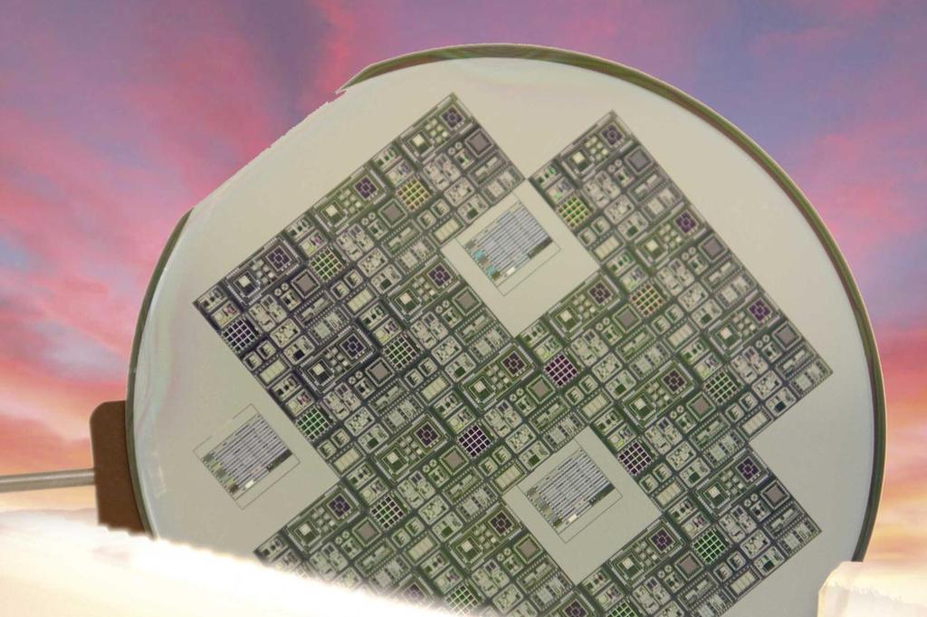
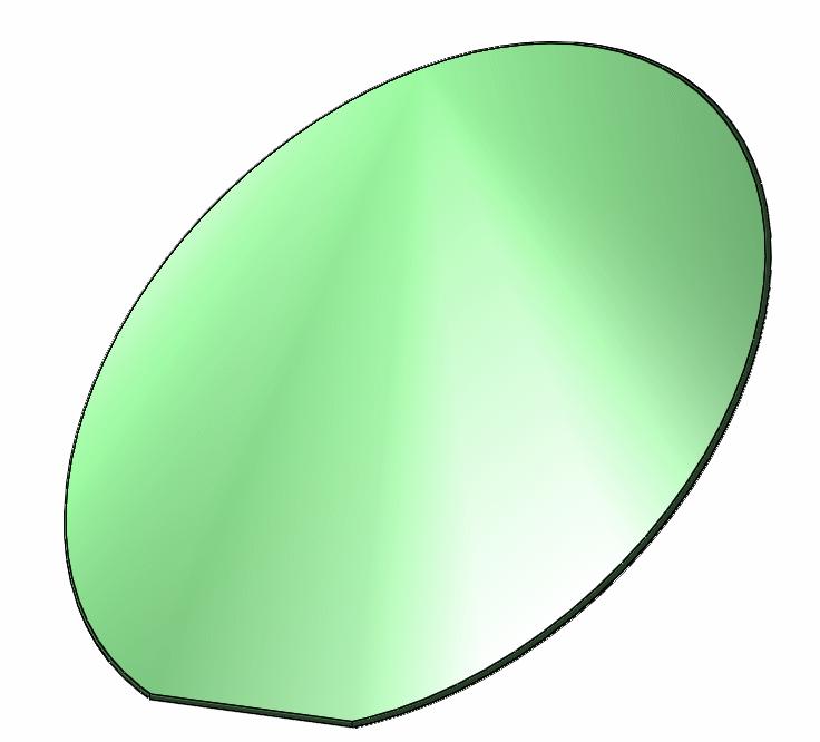
11 IC fabrication characteristics; 1 - planar technology Device area Production area 450 mm 300 mm Small devices on a large production area. 250 µm The planar surface of a silicon wafer is processed in a sequence of process steps that result in a large number of devices on the wafer surface. 100 mm 200 mm 12
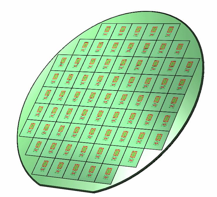

12 IC fabrication characteristics; 1 - planar technology Device area Production area 13

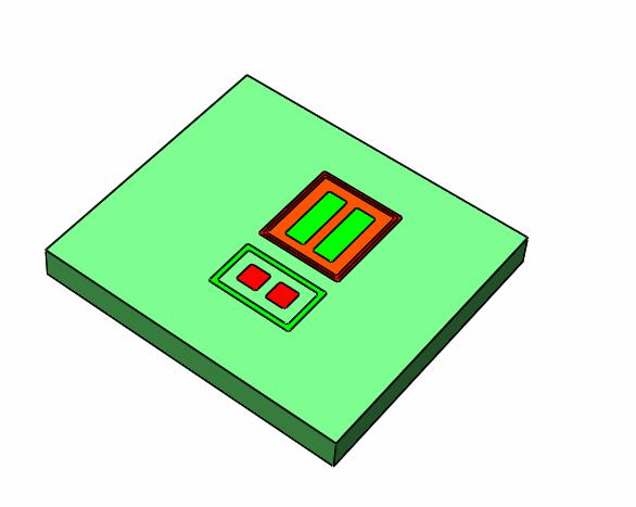
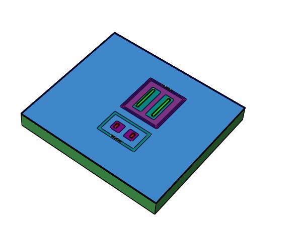
13 IC fabrication characteristics; 2 parallel processing Device area Production area 14
14 IC manufacturing: a precisely defined sequence of process modules Production area Process module #1 Process module #2 Process module #3 Process module #4 Process module #5 The set of process modules is called a flowchart: Compare it with a cookbook 15

15 Process flow How to cook an integrated circuit Flowchart STARTING MATERIAL COATING AND BAKING wafer ALIGNMENT AND EXPOSURE: Alignment makers wafer WRITE WAFER ID wafer DEVELOPMENT wafer INSPECTION: LINEWIDTH AND OVERLAY wafer DRY ETCHING: URK_NPD wafer RHOTORESIST REMOVAL: Tepla wafer CLEANING PROCEDURE: HNO3 100% and 65% (Si) wafer DRY OXIDATION: DIRT BARRIER wafer MEASUREMENT: OXIDE THICKNESS wafer COATING AND BAKING wafer ALIGNMENT AND EXPOSURE-NW wafer DEVELOPMENT wafer INSPECTION: LINEWIDTH AND OVERLAY wafer Phosporus IMPLANTATION: N-WELL wafer Phosporus IMPLANTATION: N-WELL wafer CLEANING PROCEDURE: Tepla + HNO3 100% and 65% (Si) wafer ANNEALING/NW-WELL DRIVE IN wafer MEASUREMENT: OXIDE THICKNES wafer OXIDE STRIPPING wafer CLEANING PROCEDURE: HNO3 100% and 65% (Si) wafer DRY OXIDATION: DIRT BARRIER wafer MEASUREMENT: OXIDE THICKNESS wafer COATING AND BAKING wafer ALIGNMENT AND EXPOSURE-SN wafer DEVELOPMENT wafer INSPECTION: LINEWIDTH AND OVERLAY wafer ARSENIC IMPLANTATION: NPN-EMITTER AND N-MOS SOURCE/DRAIN wafer CLEANING PROCEDURE: Tepla + HNO3 100% and 65% (Si) wafer COATING AND BAKING wafer ALIGNMENT AND EXPOSURE-SP wafer DEVELOPMENT wafer INSPECTION: LINEWIDTH AND OVERLAY wafer BORON IMPLANTATION: INTRINSIC BASE AND PMOS SOURCE/DRAIN EXTENSIONS wafer CLEANING PROCEDURE: Tepla + HNO3 100% and 65% (Si) wafer COATING AND BAKING wafer ALIGNMENT AND EXPOSURE wafer DEVELOPMENT wafer BORON IMPLANTATION: Vt ADJUST_BOTTOM HALF wafer CLEANING PROCEDURE: Tepla + HNO3 100% and 65% (Si) wafer COATING AND BAKING wafer ALIGNMENT AND EXPOSURE wafer DEVELOPMENT wafer BORON IMPLANTATION: Vt ADJUST_RIGHT HALF wafer CLEANING PROCEDURE: Tepla + HNO3 100% and 65% (Si) wafer ANNEAL / OXIDATION wafer MEASUREMENT: OXIDE THICKNESS wafer COATING AND BACKING wafer ALIGNMENT AND EXPOSURE - Oxide thickness adjust wafer DEVELOPMENT wafer INSPECTION: LINEWIDTH AND OVERLAY wafer WET WTCHING SiO2 wafer CLEANING PROCEDURE: Acetone + HNO3 100%(Si) wafer COATING AND BAKING wafer ALIGNMENT AND EXPOSURE-CO wafer DEVELOPMENT wafer INSPECTION: LINEWIDTH AND OVERLAY wafer WINDOW ETCHING wafer CLEANING PROCEDURE: Acetone + HNO3 100% and HNO3 65% (Si) wafer MARANGONI wafer FIRST METALLIZATION: SPUTTERING OF Al/Si wafer COATING AND BAKING wafer ALIGNMENT AND EXPOSURE-IC wafer DEVELOPMENT wafer INSPECTION: LINEWIDTH AND OVERLAY wafer WET ALUMINIUM ETCHING: 1 ST METAL wafer POLY SILICON DIP ETCHING wafer PLASMA ETCH ALUMINIUM: 1 st METAL wafer CLEANING PROCEDURE (after dry etching): Tepla wafer CLEANING PROCEDURE (after wet etching): Acetone wafer CLEANING PROCEDURE: HNO3 100% metal wafer ALLOYING wafer ELECTRICAL CHARACTERIZATION wafer
16 How to write a flowchart 1. Introduction 2. Flowchart elements: process blocks, modules and steps 3. Making a flowchart 17
17 Flowchart Hierarchy: Process blocks, modules and steps Definition process flowchart: A process flowchart is a connected sequence of process blocks, process modules and process steps to fabricate a device Definition process block: A process block is a connected sequence of process procedures and process steps which helps you to get the desired process target Definition process Module: A process procedure is a connected sequence of process steps to prepare the substrate(s) for the next process procedure or process step, or to terminate the process flow. Definition process step: A process step is a connected sequence of physical and/or chemical reactions used by a process tool to pattern, deposit, modify or remove materials 18


18 Flowchart Hierarchy: Process blocks, modules and steps Device level Device component level Tool level Physical / chemical process level 19
19 IC process flowcharts: example of a process block Flowchart Process block Process module Process steps Example: Process block NW 8. CLEANING : HNO3 100% and 65% (Si) 9. DRY OXIDATION: DIRT BARRIER 10. MEASUREMENT: OXIDE THICKNESS 11. COATING AND BAKING 12. ALIGNMENT AND EXPOSURE-NW 13. DEVELOPMENT 14. INSPECTION: LINEWIDTH AND OVERLAY 15. Phosporus IMPLANTATION: N-WELL 16. CLEANING : Tepla + HNO3 100% and 65% (Si) 17. ANNEALING/NW-WELL DRIVE IN 18. MEASUREMENT: OXIDE THICKNES 19. OXIDE STRIPPING 20
20 IC process flowcharts: example of a process block Flowchart Process block Process module Process steps Example: Process block NW 8. CLEANING : HNO3 100% and 65% (Si) 9. DRY OXIDATION: DIRT BARRIER 10. MEASUREMENT: OXIDE THICKNESS 11. COATING AND BAKING 12. ALIGNMENT AND EXPOSURE-NW 13. DEVELOPMENT 14. INSPECTION: LINEWIDTH AND OVERLAY 15. Phosporus IMPLANTATION: N-WELL 16. CLEANING : Tepla + HNO3 100% and 65% (Si) 17. ANNEALING/NW-WELL DRIVE IN 18. MEASUREMENT: OXIDE THICKNES 19. OXIDE STRIPPING 21
21 IC process flowcharts: example of a process module Flowchart Process block Process module Process steps Example: Process module: cleaning 16. CLEANING MODULE: Tepla + HNO3 100% and 65% (Si) Plasma strip Use the Tepla plasma system to remove the photoresist in an oxygen plasma. Follow the instructions specified for the Tepla stripper, and use the quartz carrier. Use program 4: 1000 watts power 15 minutes etching. Cleaning 10 minutes in fuming nitric acid (Merck: HNO3 100% selectipur)at ambient temperature. Use wet bench "HNO3 (100%)" and the carrier with the red dot. QDR Rinse in the Quick Dump Rinser with the standard program until the resistivity is 5 MΩ. Cleaning 10 minutes in concentrated nitric acid (Merck: HNO3 65% selectipur) at 110 C. Use wet bench HNO3 (65%) and the carrier with the red dot. QDR Rinse in the Quick Dump Rinser with the standard program until the resistivity is 5 MΩ. Drying Use the uprocess Avenger with the standard program, and the white carrier with a red dot. 22
 at 110 C.")
22 IC process flowcharts: example of a process step Flowchart Process block Process module Process step Example: Process step: cleaning Cleaning 10 minutes in concentrated nitric acid (Merck: HNO3 65% selectipur) at 110 C. Use wet bench HNO3 (65%) and the carrier with the red dot. 23
23 IC process flowcharts: example of a process step Flowchart Process block Process module Process step Example: Process step: annealing/nw-well drive in Furnace no: A1 Program name: OA002 Total time: 415 min Program no: N5 PROCESS TEMPERATURE (in C) GASSES & FLOWS (in liter/min) TIME (in minutes) boat in 600 nitrogen: REMARKS stabilize 600 nitrogen: heat up +10 C/min nitrogen: oxygen: 0.3 stabilize 1150 nitrogen: oxygen: 0.3 drive-in 1150 nitrogen: oxygen: 0.3 cool down -5 C/min nitrogen: wait for operator boat out 600 nitrogen:


24 Process flow mapped on process equipment in the lab 5 patterning processes 73 process steps grouped into 8 process modules Cleaning, patterning, deposition, etching, inspection,.. 25
25 How to write a flowchart 1. Introduction 2. Flowchart elements: process blocks, modules and steps 3. Making a flowchart 26
26 Example: fabricate a metal thin film resistor on a silicon wafer Basic equation of a thin film resistor: RR = ρρ ttt LL WW Where: ρ = the resistivity of the conductive material th = film thickness L = length of the resistor W = width of the resistor What do we need? Electrical isolation of the surface On top of that: a thin conductive film (ρ, th) Pattern the thin film into a geometry (L, W) to obtain the right value for R 27
27 Example: fabricate a metal thin film resistor on a silicon wafer Basic equation of a thin film resistor: RR = ρρ ttt LL WW Design parameters Process parameters Where: ρ = the resistivity of the conductive material th = film thickness L = length of the resistor W = width of the resistor ρρ ttt Material properties Process tool settings Flowchart components The final result of a process = R Which depends on design and processing 28
 CMOS compatible thin film resistor: ->material of choice is AlSi(1%) Estimated minimum reliable")
28 Draft a layout Boundary conditions: RR = ρρ ttt LL WW = 100 Ω Max. footprint = 200 x 500 µm Two bondpads of 80x80 µm each (neglect the bondwire/bondpad resistance) CMOS compatible thin film resistor: ->material of choice is AlSi(1%) Estimated minimum reliable thickness for wirebonding is 200 nm Minimum line width is 5 µm LL = RR WW ttt ρρ = [cm] -> L = 0.38 cm 29


29 Visualise the process flow in cross sections Note that cartoon are applied to emphasize specific characteristics, therefore cross sections are usually NOT drawn to scale Dhr. Rutte, prime minister of the Netherlands 30
 by sputtering Photolithography: coat resist, expose and develop Etch the AlSi(1%) Remove the photoresist")
30 Visualise the process flow in cross sections Start material, specify the required substrate Thermal oxidation of silicon Deposit AlSi(1%) by sputtering Photolithography: coat resist, expose and develop Etch the AlSi(1%) Remove the photoresist 31
 @ 350 C 4 COATING 5 ALIGNMENT AND EXPOSURE 6 DEVELOPING 7 PLASMA ETCHING: 200 nm Aluminium (sputtered at 350 C) 8 LAYER STRIPPING:")
31 Translate the process flow in cross sections to process modules Process overview 1 STARTING MATERIAL 2 THERMAL OXIDATION 3 METALLIZATION: 200 nm Al (with 1% 350 C 4 COATING 5 ALIGNMENT AND EXPOSURE 6 DEVELOPING 7 PLASMA ETCHING: 200 nm Aluminium (sputtered at 350 C) 8 LAYER STRIPPING: Photoresist 32
32 Feedback from your supervisor/mentor Process overview 1 STARTING MATERIAL 2 THERMAL OXIDATION 3 METALLIZATION: 200 nm Al (with 1% 350 C 4 COATING 5 ALIGNMENT AND EXPOSURE 6 DEVELOPING 7 PLASMA ETCHING: 200 nm Aluminium (sputtered at 350 C) 8 LAYER STRIPPING: Photoresist Extra process blocks added, based on experience and way of working,. Process overview 1 STARTING MATERIAL 2 CLEANING: HNO3 99% and 69.5% 3 THERMAL OXIDATION 4 MEASUREMENT: Oxide thickness 5 METALLIZATION: 200 nm Al (with 1% 350 C 6 COATING 7 ALIGNMENT AND EXPOSURE 8 DEVELOPING 9 INSPECTION: Linewidth and overlay 10 PLASMA ETCHING: 200 nm Aluminium (sputtered at 350 C) 11 ALUMINIUM FENCE REMOVAL 12 LAYER STRIPPING: Photoresist 33
33 From process modules to flowchart Each process block represents a sequence of process modules and process steps Process module Process overview 1 STARTING MATERIAL 2 CLEANING: HNO3 99% and 69.5% 3 THERMAL OXIDATION 2 CLEANING: HNO3 99% and 69.5% Process step 4 MEASUREMENT: Oxide thickness 5 METALLIZATION: 200 nm Al (with 1% 350 Clean C 10 minutes in fuming nitric acid at ambient temperature. This will dissolve 6 COATING organic materials. 7 ALIGNMENT AND EXPOSURE Use wet bench "HNO3 99% (Si)" and the carrier with the red dot. 8 DEVELOPING Rinse Rinse in the Quick Dump Rinser with the standard program until the 9 INSPECTION: Linewidth and overlay resistivity is 5 MW. 10 PLASMA ETCHING: 200 nm Aluminium (sputtered Clean at C) minutes in concentrated nitric acid at 110 C. This will dissolve metal 11 ALUMINIUM FENCE REMOVAL particles. 12 LAYER STRIPPING: Photoresist Use wet bench HNO % 110C and the carrier with the red dot. Rinse Rinse in the Quick Dump Rinser with the standard program until the resistivity is 5 MW. Dry Use the Avenger Ultra pure-6 "rinser/dryer" with the standard program, and the white carrier with a red dot. Note The next step must be performed immediately after drying. 34
 wafers, with the following specifications: Type: p/b (p-type, boron) Orientation: <100> Resistivity: 2-5 Ωcm Thickness: 525 ± 15 µm")
34 Flowchart peer review The whole flowchart is reviewed with your supervisor/mentor, special attention is given to avoid cross contamination 1. STARTING MATERIAL Use SINGLE SIDE polished LOW RESISTIVITY (LRES) wafers, with the following specifications: Type: p/b (p-type, boron) Orientation: <100> Resistivity: 2-5 Ωcm Thickness: 525 ± 15 µm Diameter: 100 mm 2. CLEANING: HNO3 99% and 69.5% Clean Rinse Clean Rinse Dry Note 10 minutes in fuming nitric acid at ambient temperature. This will dissolve organic materials. Use wet bench "HNO3 99% (Si)" and the carrier with the red dot. Rinse in the Quick Dump Rinser with the standard program until the resistivity is 5 MW. 10 minutes in concentrated nitric acid at 110 C. This will dissolve metal particles. Use wet bench HNO % 110C and the carrier with the red dot. Rinse in the Quick Dump Rinser with the standard program until the resistivity is 5 MW. Use the Avenger Ultra pure-6 "rinser/dryer" with the standard program, and the white carrier with a red dot. The next step must be performed immediately after drying. 3. MARKER OXIDATION Furnace tube: C1 or D1 Program name: MARKOXB Total time: min PROCESS TEMPERATURE GASSES & FLOWS TIME REMARKS (in C) (in liter/min) (in minutes) boat in 800 nitrogen: oxygen: 0.3 stabilize 800 nitrogen: oxygen: 0.3 heat up +10 C/min nitrogen: oxygen: 0.3 stabilize 1100 nitrogen: oxygen: 0.3 oxidation 1100 oxygen: hydrogen: 3.85 cool down -5 C/min nitrogen: wait for operator boat out 600 nitrogen: Note: The total process time can reduced in the "cool down" step: the be slightly "boat out" step can be started after ± 60 minutes, when the actual temperature of the furnace will be about 800 C. 4. MEASUREMENT: Oxide thickness Use the Leitz MPV-SP measurement system for layer thickness measurements. Follow the operating instructions from the manual when using this equipment. Program: Th. SiO2 on Si, >50nm auto5pts Oxide thickness: nm nm 5. METALLIZATION: 200 nm Al (with 1% 300 C Use the TRIKON SIGMA 204 sputter coater for the deposition of an aluminium metal layer on the wafers. The target must exist of 99% Al and 1% Si, and deposition must be done at 300 C with an Ar flow of 100 sccm. Follow the operating instructions from the manual when using this machine. Use recipe AlSi_200nm_300C to obtain a 200 nm thick layer. Visual inspection: the metal layer must look shiny. 6. CLEANING: HNO3 99% metal Clean Rinse Dry 10 minutes in fuming nitric acid at ambient temperature. This will dissolve organic materials. Use wet bench "HNO3 99% (metal)" and the carrier with a red and yellow dot. Rinse in the Quick Dump Rinser with the standard program until the resistivity is 5 MW. Use the Avenger Ultra pure-6 "rinser/dryer" with the standard program, and the white carrier with a black dot. Note Do not perform a "HNO3 69,5% 110C (Si)" cleaning step! 7. COATING Use the coater station of the EVG120 system to coat the wafers with photoresist. The process consists of: a treatment with HMDS (hexamethyldisilazane) vapor, with nitrogen as a carrier gas spin coating of Shipley SPR3012 positive resist, dispensed by a pump. The approximate spinspeed is 3450 rpm. a Soft Bake (SB) at 95 C for 90 seconds an automatic Edge Bead Removal (EBR) with a solvent Always check the relative humidity (48 ± 2 %) in the room before coating, and follow the instructions for this equipment. Use program "1-Co ,4µm". 8. ALIGNMENT AND EXPOSURE Processing will be performed on the ASML PAS5500/80 automatic wafer stepper. Follow the operating instructions from the manual when using this machine. Expose mask, with the correct litho job and exposure energy (check the energy list). 9. DEVELOPING Use the developer station of the EVG120 system to develop the wafers. The process consists of: a post-exposure bake at 115 C for 90 seconds developing with Shipley MF322 with a single puddle process a hard bake at 100 C for 90 seconds Always follow the instructions for this equipment. Use program "Dev - SP". 10. INSPECTION: Linewidth and overlay Visually inspect the wafers through a microscope, and check the line width and overlay. No resist residues are allowed. 11. PLASMA ETCHING: 675 nm Aluminium (sputtered at 350 C) Use the Trikon Wmega 201 plasma etcher. Follow the operating instructions from the manual when using this machine. It is not allowed to change the process conditions and times from the etch recipe! Use sequence AL06_350 (with a platen temperature of 25 ºC) to etch the aluminium layer. Process conditions from chamber recipe AL06_350: (use for µm Al sputtered at 350 C) Step Gasses & flows Pressure Platen RF ICP RF Platen temp. Etch time 1. breakthrough HBr/Cl2 = 40/30 sccm 5 mtorr 50 W 500 W 25 C endpoint 2. bulk etch HBr/Cl2 = 40/30 sccm 5 mtorr 40 W 500 W 25 C endpoint 3. overetch HBr/Cl2 = 30/15 sccm 5 mtorr 40 W 500 W 25 C 60% of bulk INSPECTION: No aluminium residues allowed. or undercut are Note: Always perform an "ALUMINIUM FENCE REMOVAL" step after dry etching of aluminium! 12. ALUMINIUM FENCE REMOVAL Plasma strip Moisten Etching Etch time QDR Drying Use the Tepla plasma system to remove the photoresist in an oxygen plasma. Follow the instructions specified for the Tepla stripper, and use the quartz carrier. Use program 1: 1000 watts power and automatic endpoint detection + 2 min. overetching. Rinse for 1 minute in wet bench "H2O/Triton X-100 tbv Al. Ets". Use the carrier with the yellow dot. The bath contains 1 ml Triton X-100 per 5000 ml deionized water. Use wet bench "Al. ets 35 C", and the carrier with the yellow dot. 1 liter buffered aluminium etch fluid contains: 770 ml concentrated phosphorus acid (H3PO4 85%), 19 ml concentrated nitric acid (HNO3 65%), 140 ml concentrated acetic acid (CH3COOH 100%) and 71 ml deionized water 30 seconds. 75 nm of aluminium will be lost. Rinse in the Quick Dump Rinser with the standard program until the resistivity is 5 MW. Use the Semitool "rinser/dryer" with the standard program, and the orange carrier with a black dot. 13. LAYER STRIPPING: Photoresist Strip resist Use the Tepla Plasma 300 system to remove the photoresist in an oxygen plasma. Follow the instructions specified for the Tepla stripper, and use the quartz carrier. Use program 1: 1000 watts power and automatic endpoint detection + 2 min. overetching. 35
35 Flowchart of how to make a flowchart Device concept Visualise the process flow in cross sections Feedback Translate the process flow in cross sections to process modules Feedback From process modules to flowchart Feedback Ready Introduction to process Version 1.0

36 37
Process Flow in Cross Sections
 Process Flow in Cross Sections Process (simplified) 0. Clean wafer in nasty acids (HF, HNO 3, H 2 SO 4,...) --> wear gloves! 1. Grow 500 nm of SiO 2 (by putting the wafer in a furnace with O 2 2. Coat
Microelectronic Device Instructional Laboratory. Table of Contents
 Introduction Process Overview Microelectronic Device Instructional Laboratory Introduction Description Flowchart MOSFET Development Process Description Process Steps Cleaning Solvent Cleaning Photo Lithography
Chapter 3 CMOS processing technology
 Chapter 3 CMOS processing technology (How to make a CMOS?) Si + impurity acceptors(p-type) donors (n-type) p-type + n-type => pn junction (I-V) 3.1.1 (Wafer) Wafer = A disk of silicon (0.25 mm - 1 mm thick),
3.155J / 6.152J Micro/Nano Processing Technology TAKE-HOME QUIZ FALL TERM 2005
 3.155J / 6.152J Micro/Nano Processing Technology TAKE-HOME QUIZ FALL TERM 2005 1) This is an open book, take-home quiz. You are not to consult with other class members or anyone else. You may discuss the
MEMS Surface Fabrication
 ROCHESTER INSTITUTE OF TECHNOLOGY MICROELECTRONIC ENGINEERING MEMS Surface Fabrication Dr. Lynn Fuller webpage: http://people.rit.edu/lffeee Electrical and Microelectronic Engineering Rochester Institute
Czochralski Crystal Growth
 Czochralski Crystal Growth Crystal Pulling Crystal Ingots Shaping and Polishing 300 mm wafer 1 2 Advantage of larger diameter wafers Wafer area larger Chip area larger 3 4 Large-Diameter Wafer Handling
Microelectronics. Integrated circuits. Introduction to the IC technology M.Rencz 11 September, Expected decrease in line width
 Microelectronics Introduction to the IC technology M.Rencz 11 September, 2002 9/16/02 1/37 Integrated circuits Development is controlled by the roadmaps. Self-fulfilling predictions for the tendencies
Chapter 3 Silicon Device Fabrication Technology
 Chapter 3 Silicon Device Fabrication Technology Over 10 15 transistors (or 100,000 for every person in the world) are manufactured every year. VLSI (Very Large Scale Integration) ULSI (Ultra Large Scale
EE40 Lec 22. IC Fabrication Technology. Prof. Nathan Cheung 11/19/2009
 Suggested Reading EE40 Lec 22 IC Fabrication Technology Prof. Nathan Cheung 11/19/2009 300mm Fab Tour http://www-03.ibm.com/technology/manufacturing/technology_tour_300mm_foundry.html Overview of IC Technology
Chapter 2 Manufacturing Process
 Digital Integrated Circuits A Design Perspective Chapter 2 Manufacturing Process 1 CMOS Process 2 CMOS Process (n-well) Both NMOS and PMOS must be built in the same silicon material. PMOS in n-well NMOS
Fabrication Process. Crystal Growth Doping Deposition Patterning Lithography Oxidation Ion Implementation CONCORDIA VLSI DESIGN LAB
 Fabrication Process Crystal Growth Doping Deposition Patterning Lithography Oxidation Ion Implementation 1 Fabrication- CMOS Process Starting Material Preparation 1. Produce Metallurgical Grade Silicon
EECS130 Integrated Circuit Devices
 EECS130 Integrated Circuit Devices Professor Ali Javey 9/13/2007 Fabrication Technology Lecture 1 Silicon Device Fabrication Technology Over 10 15 transistors (or 100,000 for every person in the world)
INTEGRATED-CIRCUIT TECHNOLOGY
 INTEGRATED-CIRCUIT TECHNOLOGY 0. Silicon crystal growth and wafer preparation 1. Processing Steps 1.1. Photolitography 1.2. Oxidation 1.3. Layer Deposition 1.4. Etching 1.5. Diffusion 1.6 Backend: assembly,
The Physical Structure (NMOS)
") The Physical Structure (NMOS) Al SiO2 Field Oxide Gate oxide S n+ Polysilicon Gate Al SiO2 SiO2 D n+ L channel P Substrate Field Oxide contact Metal (S) n+ (G) L W n+ (D) Poly 1 3D Perspective 2 3 Fabrication
The Physical Structure (NMOS) Al SiO2 Field Oxide Gate oxide S n+ Polysilicon Gate Al SiO2 SiO2 D n+ L channel P Substrate Field Oxide contact Metal (S) n+ (G) L W n+ (D) Poly 1 3D Perspective 2 3 Fabrication
ECE 440 Lecture 27 : Equilibrium P-N Junctions I Class Outline:
 ECE 440 Lecture 27 : Equilibrium P-N Junctions I Class Outline: Fabrication of p-n junctions Contact Potential Things you should know when you leave Key Questions What are the necessary steps to fabricate
Fabrication Technology
 Fabrication Technology By B.G.Balagangadhar Department of Electronics and Communication Ghousia College of Engineering, Ramanagaram 1 OUTLINE Introduction Why Silicon The purity of Silicon Czochralski
Semiconductor Device Fabrication
 5 May 2003 Review Homework 6 Semiconductor Device Fabrication William Shockley, 1945 The network before the internet Bell Labs established a group to develop a semiconductor replacement for the vacuum
3.155J / 6.152J MICROELECTRONICS PROCESSING TECHNOLOGY TAKE-HOME QUIZ FALL TERM 2003
 3.155J / 6.152J MICROELECTRONICS PROCESSING TECHNOLOGY TAKE-HOME QUIZ FALL TERM 2003 1) This is an open book, take-home quiz. You are not to consult with other class members or anyone else. You may discuss
Lab #2 Wafer Cleaning (RCA cleaning)
") Lab #2 Wafer Cleaning (RCA cleaning) RCA Cleaning System Used: Wet Bench 1, Bay1, Nanofabrication Center Chemicals Used: H 2 O : NH 4 OH : H 2 O 2 (5 : 1 : 1) H 2 O : HF (10 : 1) H 2 O : HCl : H 2 O 2
Lab #2 Wafer Cleaning (RCA cleaning) RCA Cleaning System Used: Wet Bench 1, Bay1, Nanofabrication Center Chemicals Used: H 2 O : NH 4 OH : H 2 O 2 (5 : 1 : 1) H 2 O : HF (10 : 1) H 2 O : HCl : H 2 O 2
All fabrication was performed on Si wafers with 285 nm of thermally grown oxide to
 Supporting Information: Substrate preparation and SLG growth: All fabrication was performed on Si wafers with 285 nm of thermally grown oxide to aid in visual inspection of the graphene samples. Prior
Lecture #18 Fabrication OUTLINE
 Transistors on a Chip Lecture #18 Fabrication OUTLINE IC Fabrication Technology Introduction the task at hand Doping Oxidation Thin-film deposition Lithography Etch Lithography trends Plasma processing
Surface micromachining and Process flow part 1
 Surface micromachining and Process flow part 1 Identify the basic steps of a generic surface micromachining process Identify the critical requirements needed to create a MEMS using surface micromachining
CMOS Technology. Flow varies with process types & company. Start with substrate selection. N-Well CMOS Twin-Well CMOS STI
 CMOS Technology Flow varies with process types & company N-Well CMOS Twin-Well CMOS STI Start with substrate selection Type: n or p Doping level, resistivity Orientation, 100, or 101, etc Other parameters
EE 330 Lecture 9. IC Fabrication Technology Part 2
 EE 330 Lecture 9 IC Fabrication Technology Part 2 Quiz 8 A 2m silicon crystal is cut into wafers using a wire saw. If the wire diameter is 220um and the wafer thickness is 350um, how many wafers will this
Total Points = 110 possible (graded out of 100)
") Lab Report 1 Table of Contents 1. Profiles & Layout (9 Points) 2. Process Procedures (20 points) 3. Calculations (36 Points) 4. Questions (35 Points) 5. Bonus Questions (10 Points) Total Points = 110 possible
Lab Report 1 Table of Contents 1. Profiles & Layout (9 Points) 2. Process Procedures (20 points) 3. Calculations (36 Points) 4. Questions (35 Points) 5. Bonus Questions (10 Points) Total Points = 110 possible
Complexity of IC Metallization. Early 21 st Century IC Technology
 EECS 42 Introduction to Digital Electronics Lecture # 25 Microfabrication Handout of This Lecture. Today: how are Integrated Circuits made? Silicon wafers Oxide formation by growth or deposition Other
Lect. 2: Basics of Si Technology
 Unit processes Thin Film Deposition Etching Ion Implantation Photolithography Chemical Mechanical Polishing 1. Thin Film Deposition Layer of materials ranging from fractions of nanometer to several micro-meters
Report 1. B. Starting Wafer Specs Number: 10 Total, 6 Device and 4 Test wafers
 Aaron Pederson EE 432 Lab Dr. Meng Lu netid: abp250 Lab instructor: Yunfei Zhao Report 1 A. Overview The goal of this lab is to go through the semiconductor fabrication process from start to finish. This
This Appendix discusses the main IC fabrication processes.
 IC Fabrication B B.1 Introduction This Appendix discusses the main IC fabrication processes. B.2 NMOS fabrication NMOS transistors are formed in a p-type substrate. The NMOS fabrication process requires
Microfabrication of Integrated Circuits
 Microfabrication of Integrated Circuits OUTLINE History Basic Processes Implant; Oxidation; Photolithography; Masks Layout and Process Flow Device Cross Section Evolution Lecture 38, 12/05/05 Reading This
UT Austin, ECE Department VLSI Design 2. CMOS Fabrication, Layout Rules
 2. CMOS Fabrication, Layout, Design Rules Last module: Introduction to the course How a transistor works CMOS transistors This module: CMOS Fabrication Design Rules CMOS Fabrication CMOS transistors are
Lecture 0: Introduction
 Lecture 0: Introduction Introduction Integrated circuits: many transistors on one chip. Very Large Scale Integration (VLSI): bucketloads! Complementary Metal Oxide Semiconductor Fast, cheap, low power
EE 5344 Introduction to MEMS. CHAPTER 3 Conventional Si Processing
 3. Conventional licon Processing Micromachining, Microfabrication. EE 5344 Introduction to MEMS CHAPTER 3 Conventional Processing Why silicon? Abundant, cheap, easy to process. licon planar Integrated
CyMOS process Spring 2016 Iowa State University
 CyMOS process Spring 2016 Iowa State University Start Date Starting Material Orientation: Dopant: Resistivity: Ω cm Doping Concentration: cm 3 Diameter: inch Thickness: µm Lot Identification: Wafer Count
PROCESS FLOW AN INSIGHT INTO CMOS FABRICATION PROCESS
 Contents: VI Sem ECE 06EC63: Analog and Mixed Mode VLSI Design PROCESS FLOW AN INSIGHT INTO CMOS FABRICATION PROCESS 1. Introduction 2. CMOS Fabrication 3. Simplified View of Fabrication Process 3.1 Alternative
Bulk MEMS Fabrication Details Dr. Lynn Fuller, Casey Gonta, Patsy Cadareanu
 ROCHESTER INSTITUTE OF TECHNOLOGY MICROELECTRONIC ENGINEERING Bulk MEMS Fabrication Details Dr. Lynn Fuller, Casey Gonta, Patsy Cadareanu Webpage: http://people.rit.edu/lffeee 82 Lomb Memorial Drive Rochester,
CMOS Manufacturing process. Design rule set
 CMOS Manufacturing process Circuit design Set of optical masks Fabrication process Circuit designer Design rule set Process engineer All material: Chap. 2 of J. Rabaey, A. Chandrakasan, B. Nikolic, Digital
Fabrication and Layout
 ECEN454 Digital Integrated Circuit Design Fabrication and Layout ECEN 454 3.1 A Glimpse at MOS Device Polysilicon Aluminum ECEN 475 4.2 1 Material Classification Insulators Glass, diamond, silicon oxide
FABRICATION of MOSFETs
 FABRICATION of MOSFETs CMOS fabrication sequence -p-type silicon substrate wafer -creation of n-well regions for pmos transistors, -impurity implantation into the substrate. -thick oxide is grown in the
EE 330 Lecture 8. IC Fabrication Technology Part II. - Masking - Photolithography - Deposition - Etching - Diffusion
 EE 330 Lecture 8 IC Fabrication Technology Part II?? - Masking - Photolithography - Deposition - Etching - Diffusion Review from Last Time Technology Files Provide Information About Process Process Flow
Lecture 1A: Manufacturing& Layout
 Introduction to CMOS VLSI Design Lecture 1A: Manufacturing& Layout David Harris Harvey Mudd College Spring 2004 Steven Levitan Fall 2008 1 The Manufacturing Process For a great tour through the IC manufacturing
PHYS 534 (Fall 2008) Process Integration OUTLINE. Examples of PROCESS FLOW SEQUENCES. >Surface-Micromachined Beam
 Process Integration OUTLINE. Examples of PROCESS FLOW SEQUENCES. >Surface-Micromachined Beam") PHYS 534 (Fall 2008) Process Integration Srikar Vengallatore, McGill University 1 OUTLINE Examples of PROCESS FLOW SEQUENCES >Semiconductor diode >Surface-Micromachined Beam Critical Issues in Process
PHYS 534 (Fall 2008) Process Integration Srikar Vengallatore, McGill University 1 OUTLINE Examples of PROCESS FLOW SEQUENCES >Semiconductor diode >Surface-Micromachined Beam Critical Issues in Process
CS/ECE 5710/6710. N-type Transistor. N-type from the top. Diffusion Mask. Polysilicon Mask. CMOS Processing
 CS/ECE 5710/6710 CMOS Processing Addison-Wesley N-type Transistor D G +Vgs + Vds S N-type from the top i electrons - Diffusion Mask Mask for just the diffused regions Top view shows patterns that make
CMOS Fabrication. Dr. Bassam Jamil. Adopted from slides of the textbook
 CMOS Fabrication Dr. Bassam Jamil Adopted from slides of the textbook CMOS Fabrication CMOS transistors are fabricated on silicon wafer Lithography process similar to printing press On each step, different
ELEC 3908, Physical Electronics, Lecture 4. Basic Integrated Circuit Processing
 ELEC 3908, Physical Electronics, Lecture 4 Basic Integrated Circuit Processing Lecture Outline Details of the physical structure of devices will be very important in developing models for electrical behavior
VLSI INTRODUCTION P.VIDYA SAGAR ( ASSOCIATE PROFESSOR) Department of Electronics and Communication Engineering, VBIT
 Department of Electronics and Communication Engineering, VBIT") VLSI INTRODUCTION P.VIDYA SAGAR ( ASSOCIATE PROFESSOR) contents UNIT I INTRODUCTION: Introduction to IC Technology MOS, PMOS, NMOS, CMOS & BiCMOS technologies. BASIC ELECTRICAL PROPERTIES : Basic Electrical
VLSI INTRODUCTION P.VIDYA SAGAR ( ASSOCIATE PROFESSOR) contents UNIT I INTRODUCTION: Introduction to IC Technology MOS, PMOS, NMOS, CMOS & BiCMOS technologies. BASIC ELECTRICAL PROPERTIES : Basic Electrical
Semiconductor Manufacturing Technology. IC Fabrication Process Overview
 Semiconductor Manufacturing Technology Michael Quirk & Julian Serda October 00 by Prentice Hall Chapter 9 IC Fabrication Process Overview /4 Objectives After studying the material in this chapter, you
FABRICATION OF CMOS INTEGRATED CIRCUITS. Dr. Mohammed M. Farag
 FABRICATION OF CMOS INTEGRATED CIRCUITS Dr. Mohammed M. Farag Outline Overview of CMOS Fabrication Processes The CMOS Fabrication Process Flow Design Rules EE 432 VLSI Modeling and Design 2 CMOS Fabrication
Review of CMOS Processing Technology
 - Scaling and Integration Moore s Law Unit processes Thin Film Deposition Etching Ion Implantation Photolithography Chemical Mechanical Polishing 1. Thin Film Deposition Layer of materials ranging from
EE 432/532 CyMOS process PWELL Lithography & Diffusion Feb 24, 2016
 EE 432/532 CyMOS process PWELL Lithography & Diffusion Feb 24, 2016 Friday Afternoon Group Brady Koht Sebastian Roe Peter Bonnie Joseph Wickner Lab Instructor Yunfei Zhao 1. Overview Now that a Field Oxide
Lecture 19 Microfabrication 4/1/03 Prof. Andy Neureuther
 EECS 40 Spring 2003 Lecture 19 Microfabrication 4/1/03 Prof. ndy Neureuther How are Integrated Circuits made? Silicon wafers Oxide formation by growth or deposition Other films Pattern transfer by lithography
Department of Electrical Engineering. Jungli, Taiwan
 Chapter 3 Fabrication of CMOS Integrated Circuits Jin-Fu Li Department of Electrical Engineering National Central University Jungli, Taiwan Background Outline The CMOS Process Flow Design Rules Latchup
Figure 2.3 (cont., p. 60) (e) Block diagram of Pentium 4 processor with 42 million transistors (2000). [Courtesy Intel Corporation.
 (e) Block diagram of Pentium 4 processor with 42 million transistors (2000). [Courtesy Intel Corporation.") Figure 2.1 (p. 58) Basic fabrication steps in the silicon planar process: (a) oxide formation, (b) selective oxide removal, (c) deposition of dopant atoms on wafer, (d) diffusion of dopant atoms into exposed
Figure 2.1 (p. 58) Basic fabrication steps in the silicon planar process: (a) oxide formation, (b) selective oxide removal, (c) deposition of dopant atoms on wafer, (d) diffusion of dopant atoms into exposed
Photolithography I ( Part 2 )
") 1 Photolithography I ( Part 2 ) Chapter 13 : Semiconductor Manufacturing Technology by M. Quirk & J. Serda Bjørn-Ove Fimland, Department of Electronics and Telecommunication, Norwegian University of Science
1 Photolithography I ( Part 2 ) Chapter 13 : Semiconductor Manufacturing Technology by M. Quirk & J. Serda Bjørn-Ove Fimland, Department of Electronics and Telecommunication, Norwegian University of Science
EE432/532 CYMOS PROCESS PWELL LITHOGRAPHY AND DIFFUSION
 EE432/532 CYMOS PROCESS PWELL LITHOGRAPHY AND DIFFUSION [Document subtitle] GROUP 4 GROUP 4 (TUESDAY AFTERNOON) GROUP LEADER: ANDREW MCNEIL GROUP MEMBERS: WENG HOONG LOO MARIO PEREZ ZHIHAO LIAO LAB INSTRUCTOR
EE 143 FINAL EXAM NAME C. Nguyen May 10, Signature:
 INSTRUCTIONS Read all of the instructions and all of the questions before beginning the exam. There are 5 problems on this Final Exam, totaling 143 points. The tentative credit for each part is given to
EE 330 Lecture 9. IC Fabrication Technology Part II. -Oxidation -Epitaxy -Polysilicon -Planarization -Resistance and Capacitance in Interconnects
 EE 330 Lecture 9 IC Fabrication Technology Part II -Oxidation -Epitaxy -Polysilicon -Planarization -Resistance and Capacitance in Interconnects Review from Last Time IC Fabrication Technology Crystal Preparation
EE 143 CMOS Process Flow
 EE 143 CMOS rocess Flow CT 84 D D G Sub G Sub S S G D S G D S + + + + - MOS Substrate Well - MOS Substrate EE 143 CMOS rocess Flow CT 85 hotoresist Si 3 4 SiO 2 Substrate selection: moderately high resistivity,
A discussion of crystal growth, lithography, etching, doping, and device structures is presented in
 Chapter 5 PROCESSING OF DEVICES A discussion of crystal growth, lithography, etching, doping, and device structures is presented in the following overview gures. SEMICONDUCTOR DEVICE PROCESSING: AN OVERVIEW
Photolithography Process Technology
 Contents Photolithography Process - Wafer Preparation - Photoresist Coating - Align & Expose - Photoresist Development Process Control CD Measurement Equipment Expose System & Wafer Track Consumables Chemicals
DEPARTMENT OF MECHANICAL SCIENCE AND ENGINEERING UNIVERSITY OF ILLINOIS. ME498 PV Class. Laboratory Manual on Fundamentals of Solar Cell Manufacturing
 DEPARTMENT OF MECHANICAL SCIENCE AND ENGINEERING UNIVERSITY OF ILLINOIS ME498 PV Class Laboratory Manual on Fundamentals of Solar Cell Manufacturing Prepared by Bruno Azeredo, and Dr. Elif Ertekin 9/21/2013
CHAPTER - 4 CMOS PROCESSING TECHNOLOGY
 CHAPTER - 4 CMOS PROCESSING TECHNOLOGY Samir kamal Spring 2018 4.1 CHAPTER OBJECTIVES 1. Introduce the CMOS designer to the technology that is responsible for the semiconductor devices that might be designed
4. Thermal Oxidation. a) Equipment Atmospheric Furnace
 Equipment Atmospheric Furnace") 4. Thermal Oxidation a) Equipment Atmospheric Furnace Oxidation requires precise control of: temperature, T ambient gas, G time spent at any given T & G, t Vito Logiudice 34 4. Thermal Oxidation b) Mechanism
4. Thermal Oxidation a) Equipment Atmospheric Furnace Oxidation requires precise control of: temperature, T ambient gas, G time spent at any given T & G, t Vito Logiudice 34 4. Thermal Oxidation b) Mechanism
Chapter 2 MOS Fabrication Technology
 Chapter 2 MOS Fabrication Technology Abstract This chapter is concerned with the fabrication of metal oxide semiconductor (MOS) technology. Various processes such as wafer fabrication, oxidation, mask
Nanoelectronics Fabrication Facility
 Nanoelectronics Fabrication Facility Contents Introduction 2 Mask Making Module 4 Photolithography Module 6 Wet Etching and CMP Module 8 Dry Etching and Sputtering Module 10 Thermal Process and Implantation
Introduction to CMOS VLSI Design. Layout, Fabrication, and Elementary Logic Design
 Introduction to CMOS VLSI Design Layout, Fabrication, and Elementary Logic Design CMOS Fabrication CMOS transistors are fabricated on silicon wafer Lithography process similar to printing press On each
CMOS VLSI Design. Introduction. All materials are from the textbook Weste and Harris, 3 rd Edition CMOS VLSI DESIGN. Introduction
 CMOS VLSI Design Introduction ll materials are from the textbook Weste and Harris, 3 rd Edition CMOS VLSI DESIGN Introduction Chapter previews the entire field, subsequent chapters elaborate on specific
EE 330 Lecture 8. IC Fabrication Technology Part II. - Oxidation - Epitaxy - Polysilicon - Interconnects
 EE 330 Lecture 8 IC Fabrication Technology Part II - Oxidation - Epitaxy - Polysilicon - Interconnects Review from Last Time MOS Transistor Bulk Source Gate Drain p-channel MOSFET Lightly-doped n-type
Temperature Scales. Questions. Temperature Conversions 7/21/2010. EE580 Solar Cells Todd J. Kaiser. Thermally Activated Processes
 7/1/010 EE80 Solar Cells Todd J. Kaiser Flow of Wafer in Fabrication Lecture 0 Microfabrication A combination of Applied Chemistry, Physics and ptics Thermal Processes Diffusion & xidation Photolithograpy
Mostafa Soliman, Ph.D. May 5 th 2014
 Mostafa Soliman, Ph.D. May 5 th 2014 Mostafa Soliman, Ph.D. 1 Basic MEMS Processes Front-End Processes Back-End Processes 2 Mostafa Soliman, Ph.D. Wafers Deposition Lithography Etch Chips 1- Si Substrate
Lecture 22: Integrated circuit fabrication
 Lecture 22: Integrated circuit fabrication Contents 1 Introduction 1 2 Layering 4 3 Patterning 7 4 Doping 8 4.1 Thermal diffusion......................... 10 4.2 Ion implantation.........................
EE CMOS TECHNOLOGY- Chapter 2 in the Text
 1 EE 212 FALL 1999-00 CMOS TECHOLOGY- Chapter 2 in the Text In this set of notes we will describe a modern CMOS process flow. In the simplest CMOS technologies, we need to realize simply MOS and MOS transistors
EE 560 FABRICATION OF MOS CIRCUITS. Kenneth R. Laker, University of Pennsylvania
 1 EE 560 FABRICATION OF MOS CIRCUITS 2 CMOS CHIP MANUFACTRING STEPS Substrate Wafer Wafer Fabrication (diffusion, oxidation, photomasking, ion implantation, thin film deposition, etc.) Finished Wafer Wafer
Report 2. Aaron Pederson EE 432 Lab Dr. Meng Lu netid: abp250 Lab instructor: Yunfei Zhao. Steps:
 Aaron Pederson EE 432 Lab Dr. Meng Lu netid: abp250 Lab instructor: Yunfei Zhao Report 2 A. Overview This section comprised of source and drain construction for the NMOS and PMOS. This includes two different
Lecture 2: CMOS Fabrication Mark McDermott Electrical and Computer Engineering The University of Texas at Austin
 Lecture 2: CMOS Fabrication Mark McDermott Electrical and Computer Engineering The University of Texas at Austin Agenda Last module: Introduction to the course How a transistor works CMOS transistors This
VLSI Design and Simulation
 VLSI Design and Simulation CMOS Processing Technology Topics CMOS Processing Technology Semiconductor Processing How do we make a transistor? Fabrication Process Wafer Processing Silicon single crystal
Fabrication and Layout
 Fabrication and Layout Kenneth Yun UC San Diego Adapted from EE271 notes, Stanford University Overview Semiconductor properties How chips are made Design rules for layout Reading Fabrication: W&E 3.1,
VLSI. Lecture 1. Jaeyong Chung System-on-Chips (SoC) Laboratory Incheon National University. Based on slides of David Money Harris
 Laboratory Incheon National University. Based on slides of David Money Harris") VLSI Lecture 1 Jaeyong Chung System-on-Chips (SoC) Laboratory Incheon National University Based on slides of David Money Harris Goals of This Course Learn the principles of VLSI design Learn to design
VLSI Lecture 1 Jaeyong Chung System-on-Chips (SoC) Laboratory Incheon National University Based on slides of David Money Harris Goals of This Course Learn the principles of VLSI design Learn to design
9/4/2008 GMU, ECE 680 Physical VLSI Design
 ECE680: Physical VLSI Design Chapter II CMOS Manufacturing Process 1 Dual-Well Trench-Isolated CMOS Process gate-oxide TiSi 2 AlCu Tungsten SiO 2 p-well poly n-well SiO 2 n+ p-epi p+ p+ 2 Schematic Layout
Complementary Metal-Oxide-Semiconductor Very Large-Scale Integrated Circuit Design
 Complementary Metal-Oxide-Semiconductor Very Large-Scale Integrated Circuit Design Bradley A. Minch Mixed Analog-Digital VLSI Circuits and Systems Lab Cornell University Ithaca, NY 14853 5401 minch@ece.cornell.edu
6.777J/2.732J Design and Fabrication of Microelectromechanical Devices Spring Term Solution to Problem Set 2 (16 pts)
") 6.777J/2.732J Design and Fabrication of Microelectromechanical Devices Spring Term 2007 By Brian Taff (Adapted from work by Feras Eid) Solution to Problem Set 2 (16 pts) Issued: Lecture 4 Due: Lecture
6.777J/2.732J Design and Fabrication of Microelectromechanical Devices Spring Term 2007 By Brian Taff (Adapted from work by Feras Eid) Solution to Problem Set 2 (16 pts) Issued: Lecture 4 Due: Lecture
Supporting Information: Model Based Design of a Microfluidic. Mixer Driven by Induced Charge Electroosmosis
 Supporting Information: Model Based Design of a Microfluidic Mixer Driven by Induced Charge Electroosmosis Cindy K. Harnett, Yehya M. Senousy, Katherine A. Dunphy-Guzman #, Jeremy Templeton * and Michael
EE 432 CyMOS process PWELL Photolithography and Diffusion Feb. 23th 2017
 1 EE 432 CyMOS process PWELL Photolithography and Diffusion Feb. 23th 2017 Group III Jake Asmus (Leader) John Guss Shengliang Liu Xin Chen Lab instructor Matt Weinstein 2 Overview With the field oxide
Metallization deposition and etching. Material mainly taken from Campbell, UCCS
 Metallization deposition and etching Material mainly taken from Campbell, UCCS Application Metallization is back-end processing Metals used are aluminum and copper Mainly involves deposition and etching,
Manufacturing Process
 Manufacturing Process 1 CMOS Process 2 A Modern CMOS Process gate-oxide TiSi 2 AlCu Tungsten SiO 2 n+ p-well p-epi poly n-well p+ SiO 2 p+ Dual-Well Trench-Isolated CMOS Process 3 Single-crystal ingot
5.8 Diaphragm Uniaxial Optical Accelerometer
 5.8 Diaphragm Uniaxial Optical Accelerometer Optical accelerometers are based on the BESOI (Bond and Etch back Silicon On Insulator) wafers, supplied by Shin-Etsu with (100) orientation, 4 diameter and
Microstructure of Electronic Materials. Amorphous materials. Single-Crystal Material. Professor N Cheung, U.C. Berkeley
 Microstructure of Electronic Materials Amorphous materials Single-Crystal Material 1 The Si Atom The Si Crystal diamond structure High-performance semiconductor devices require defect-free crystals 2 Crystallographic
Most semiconductor devices contain at least one junction between p-type and n-type material. These p-n junctions are fundamental to the performance
 Ch. 5: p-n Junction Most semiconductor devices contain at least one junction between p-type and n-type material. These p-n junctions are fundamental to the performance of functions such as rectification,
micro resist technology
 Characteristics Processing guidelines Negative Tone Photoresist Series ma-n 1400 ma-n 1400 is a negative tone photoresist series designed for the use in microelectronics and microsystems. The resists are
Surface MEMS Fabrication Details Dr. Lynn Fuller, Adam Wardas, Casey Gonta, Patsy Cadareanu
 ROCHESTER INSTITUTE OF TECHNOLOGY MICROELECTRONIC ENGINEERING Surface MEMS Fabrication Details Dr. Lynn Fuller, Adam Wardas, Casey Gonta, Patsy Cadareanu Webpage: http://people.rit.edu/lffeee 82 Lomb Memorial
Make sure the exam paper has 9 pages total (including cover page)
") UNIVERSITY OF CALIFORNIA College of Engineering Department of Electrical Engineering and Computer Sciences Fall 2010 EE143 Midterm Exam #2 Family Name First name SID Signature Solution Make sure the exam
UNIVERSITY OF CALIFORNIA College of Engineering Department of Electrical Engineering and Computer Sciences Fall 2010 EE143 Midterm Exam #2 Family Name First name SID Signature Solution Make sure the exam
Physical Vapor Deposition (PVD) Zheng Yang
 Zheng Yang") Physical Vapor Deposition (PVD) Zheng Yang ERF 3017, email: yangzhen@uic.edu Page 1 Major Fabrication Steps in MOS Process Flow UV light Mask oxygen Silicon dioxide photoresist exposed photoresist oxide
Physical Vapor Deposition (PVD) Zheng Yang ERF 3017, email: yangzhen@uic.edu Page 1 Major Fabrication Steps in MOS Process Flow UV light Mask oxygen Silicon dioxide photoresist exposed photoresist oxide
IC/MEMS Fabrication - Outline. Fabrication
 IC/MEMS Fabrication - Outline Fabrication overview Materials Wafer fabrication The Cycle: Deposition Lithography Etching Fabrication IC Fabrication Deposition Spin Casting PVD physical vapor deposition
CMOS FABRICATION. n WELL PROCESS
 CMOS FABRICATION n WELL PROCESS Step 1: Si Substrate Start with p- type substrate p substrate Step 2: Oxidation Exposing to high-purity oxygen and hydrogen at approx. 1000 o C in oxidation furnace SiO
EE 527 MICROFABRICATION. Lecture 15 Tai-Chang Chen University of Washington EE-527 M4 MASK SET: NPN BJT. C (sub) A E = 40 µm x 40 µm
 A E = 40 µm x 40 µm") EE 527 MICROFABRICATION Lecture 15 Tai-Chang Chen University of Washington EE-527 M4 MASK SET: NPN BJT C (sub) E B A E = 40 µm x 40 µm 1 EE-527 M4 MASK SET: MOS C-V TEST CAPACITORS W = 10 µm L = 10 µm
EE 527 MICROFABRICATION Lecture 15 Tai-Chang Chen University of Washington EE-527 M4 MASK SET: NPN BJT C (sub) E B A E = 40 µm x 40 µm 1 EE-527 M4 MASK SET: MOS C-V TEST CAPACITORS W = 10 µm L = 10 µm