Integrated Process Technology Development for the sub 7nm Era
|
|
|
- Sara Merritt
- 6 years ago
- Views:
Transcription
1 Integrated Process Technology Development for the sub 7nm Era July 12, 2017 Alex Oscilowski President TEL Technology Center, America, LLC.
 TEL Technology Center, America TEL Technology")

 TEL Technology Center, Taiwan IME")
2 TEL s Global R&D Operations Korea U.S. imec (Belgium) TEL Technology Center, America TEL Technology Center Korea CEA-Leti (France) Taiwan Japan Tokyo Electron Yamanashi Ltd. Tokyo Electron Kyushu Ltd. Tokyo Electron Tohoku Ltd. Tokyo Electron Miyagi Ltd. SUNY Poly/CNSE (US) TEL Technology Center, Taiwan IME (Singapore) TEL R&D base Consortium Alex Oscilowski/TTCA/July 12,
3 TEL R&D programs target key industry challenges Technology Roadmap (by Mx pitch) 64-56nm 48-40nm 38-28nm 28-20nm 20-14nm N14 N10 N7 N5 N3.5 Patterning (Logic M1 pitch) ArF immersion ArF-i/EUV/DSA SADP, LEn SADP, LEn SAQP, LEn SAQP, LEn SAOP, LEn Device FinFET FinFET FinFET FinFET, Nanowire FinFET, Nanowire Material: Channel, Contact plug, Interconnect metal Si/Si Si/Si Si/SiGe III-V/SiGe, Ge III-V/SiGe, Ge W W, Co W, Co Co Co Cu Cu Co, Cu Co, Ru Co, Ru Disruptive changes for N7/N5 Patterning methods Device architectures Material schemes are addressed through unique TTCA in Albany World class engineering talent Leading-edge process access Process/Metrology tools Competitive Benchmarking EUV Integrated flows and e-test Alex Oscilowski/TTCA/July 12,


4 TTCA R&D strategy for <7nm Develop integrated process technology modules through key R&D partnerships that deliver value to TEL and our customers Alex Oscilowski/TTCA/July 12,


 Metrology Integrated process technology modules Gate Contact")
5 Integrated process technology modules for <7nm Process Process technology technology Lithography/Patterning Lithography/Patterning Deposition Deposition Etch Etch Cleans Cleans Integration capability Test structures Wafer processing/access Test data (electrical/rel.) Metrology Integrated process technology modules Gate Contact Interconnect Alex Oscilowski/TTCA/July 12,
6 TTCA key R&D partnerships IBM alliance JDPs EUV patterning Transistor data Electrical/rel. data SUNY Poly/CNSE Infrastructure Technology FEOL materials EUV extension Transistor data Novel devices Supplier partners Customer focused R&D JDPs Advanced patterning Integrated modules Demos Internal R&D Module development Fast cycle feasibility Electrical/rel. data Test structures Wafer processing Competitive Benchmarking Alex Oscilowski/TTCA/July 12,
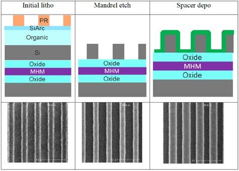
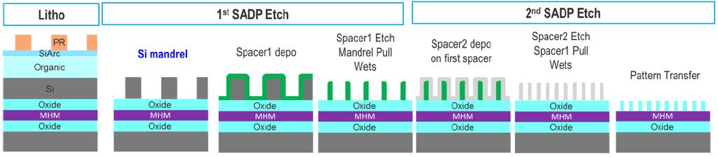
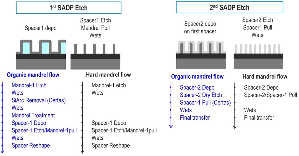
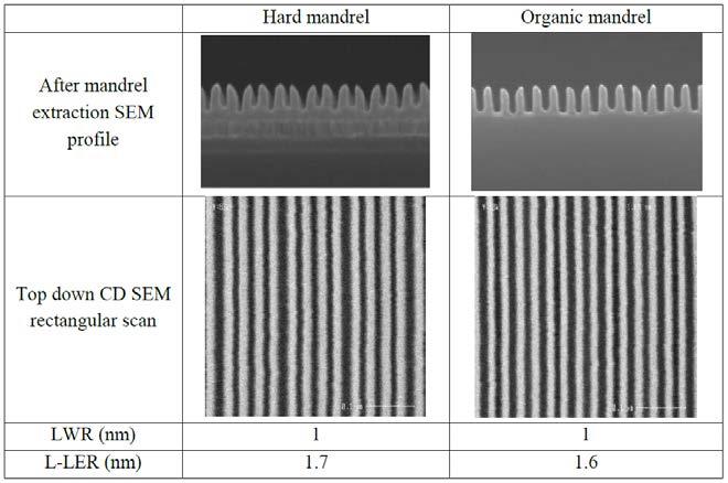
7 Advanced Patterning Examples Alex Oscilowski/TTCA/July 12,


 nm LWR/LER for 4 line and 4 space features LWR LER")

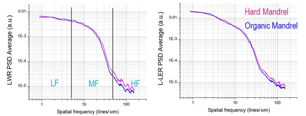
8 SAQP using a photoresist mandrel Photoresist mandrel challenge Standard Treatment 1 Treatment 2 PR PR SiARC ODL PR PR SiARC ODL SiARC ODL SiARC ODL A-Si Oxide SiN A-Si Oxide SiN A-Si Oxide SiN A-Si Oxide SiN Oxide SiN Oxide SiN Oxide SiN Si Si Mandrel hardening Si Si Si Si Si Si Improved verticality CD ~ 16.8nm; L(S) CDU ~ 0.7 (0.9) nm LWR/LER for 4 line and 4 space features LWR LER Ave line 1.5 nm 1.2 nm Ave space 0.6 nm 1.3 nm H. Kang, SMC-2017, Seoul CDU, LER comparable to double hard mandrel SAQP Alex Oscilowski/TTCA/July 12,
9 Demonstrated Spacer-on-Spacer for SAQP cost reduction Fewer Steps for Same Results: Alex Oscilowski/TTCA/July 12, S. Thibaut et al, SPIE 2017


10 Self-Aligned Block for critical sub-40nm pitch Mx patterning A. Raley et al, SPIE 2017 Alex Oscilowski/TTCA/July 12,
11 Advanced Gate Stack Examples Alex Oscilowski/TTCA/July 12,

12 Ferroelectricity in Hafnium Oxide based Thin Films Engineered HfO 2 Anneal, etc. Doped HfO 2 Zr, Al, Gd, La, Si, Sr and Y Ferroelectricity in HfO 2 origin is assumed attributed to the non centrosymmetric phase/orthorhombic phase Currently Ferroelectric films are considered for Ferroelectric RAM (FeRAM) and as gate dielectrics for negative capacitance FETs (NCFETs) Source: J. Muller, SEMICON Europa 2012 T.S. Boscke et al. Appl. Phys. Lett Alex Oscilowski/TTCA/July 12,


13 Negative Capacitance FET (NCFET) Electrical Performance I DS -V GS Characteristics Scaling effect L G = 2 μm L G = 1 μm Steep sub-threshold slope demonstrated with ALD HZO thickness scaling Steep switching only occurs when device swept beyond coercive voltage. Dipole switching is essential for onset of NC effect. Sharma et al, VLSI-2017, Kyoto Alex Oscilowski/TTCA/July 12,
14 Advanced Contact Examples Alex Oscilowski/TTCA/July 12,


15 ALD Ti vs PVD Ti: wrap around contact NMOS Si:P R FIN R C PLOTS 4Fin-TLM resistance (Ω) 4.0k 3.0k 2.0k 1.0k 0.0 ALD Ti PVD Ti + extra HF ALD Ti + extra HF Spacing (µm) ALD Ti PVD Ti + extra HF ALD Ti + extra HF ALD Ti ALD TI + Extra HF ALD Ti wafers have lower Rc as compared to PVD Ti wafers Conformal Processes for Contact Cleans and Metals enable Wrap Around Contacts Alex Oscilowski/TTCA/July 12, IITC


16 Etch Challenges for EUV Based Contact Patterning Etch Innovation required to break these tradeoffs and to help correct incoming variability TEL DC Superposition with Q-ALE Technology enable Concurrent attainment of High Selectivity Symmetric Shrink LER smoothing & and wiggle mitigation Quasi- ALE Concept / Model A. Metz, SPIE 2017 Alex Oscilowski/TTCA/July 12,
17 Advanced Interconnect Examples Alex Oscilowski/TTCA/July 12,

% = 0.")

18 Physical Characterization: ALD barrier testing: In-situ Ramp Anneals Barrier layers investigated using in-situ ramp anneal synchrotron XRD (Advanced Photon Source at Argonne National Lab) T c = 695ºC Integrated area under XRD peaks Al/(Al+Ta)% = 0.33 ALD TaN and TaAlN show better barrier performance than PVD TaN Alex Oscilowski/TTCA/July 12, S. Consiglio et al. ECS Trans Fall (2015)
![Resistance [kohm] [kohm] Electrical Characterization: ALD barrier / CVD-Ru liner (2nm) / Cu-fill 220 200 180 160 PVD-TaN 2nm](/docs-images/76/73626079/images/19-1.jpg "ALD-TaN 2nm ALD-TaN 1nm ALD-TaAlN 2nm ALD-TaAlN 1nm L/S=60nm/60nm 140 3.5 4.0 4.5 5.")
![0 Capacitance [pf] Cumulative probability [%] 99.](/docs-images/76/73626079/images/19-2.jpg "9 99 95 90 80 70 50 30 20 10 5 1 Via size=64nm PVD-TaN 2nm ALD-TaN 2nm ALD-TaN 1nm ALD-TaAlN 2nm ALD-TaAlN 1nm.")
![1 0 10 20 30 Via resistance [ohm] [kohm] Time to 50% failure [sec] 10 3 10 2 10 1 10 0 L/S=60nm/60nm peri.=30mm temp.](/docs-images/76/73626079/images/19-3.jpg "=125degc PVD-TaN 2nm ALD-TaN 2nm ALD-TaN 1nm ALD-TaAlN 2nm ALD-TaAlN 1nm TDDB 4 5 6 Electric field [MV/cm] Lower RC and Via")
19 Resistance [kohm] [kohm] Electrical Characterization: ALD barrier / CVD-Ru liner (2nm) / Cu-fill PVD-TaN 2nm ALD-TaN 2nm ALD-TaN 1nm ALD-TaAlN 2nm ALD-TaAlN 1nm L/S=60nm/60nm Capacitance [pf] Cumulative probability [%] Via size=64nm PVD-TaN 2nm ALD-TaN 2nm ALD-TaN 1nm ALD-TaAlN 2nm ALD-TaAlN 1nm Via resistance [ohm] [kohm] Time to 50% failure [sec] L/S=60nm/60nm peri.=30mm temp.=125degc PVD-TaN 2nm ALD-TaN 2nm ALD-TaN 1nm ALD-TaAlN 2nm ALD-TaAlN 1nm TDDB Electric field [MV/cm] Lower RC and Via Resistance plus Superior TDDB with ALD-Ta(Al)N compared to POR PVD-TaN Alex Oscilowski/TTCA/July 12, Y. Kikuchi et al., IITC/AMC 2016


 / Serial number 20")
20 TTCA unique capabilities Patterning capability Key R&D partnerships Rapid cycles of learning Leading edge litho ASML XT1950 ArFi- 193i ASML NXE3300B EUV DSA Film deposition, etch, and clean expertise Structures for gates, contacts, interconnects, 3DI Novel structures World class team Cross disciplinary/multi BU Breadth and depth Customer, supplier, consortia experience Joint development with all key customers, partners, suppliers on site Extensive data sharing/learning TTCA Full flow tool/process access Leading edge patterning Ge and III-V epi, BDIII, PVD, LSA/RTA Secure, TEL controlled full flow 24/7 process/tool access FEOL/MOL/BEOL/3DI All TEL/competitor tools Metrology/test Competitive Benchmarking Available to all TEL businesses Fast demo and feasibility data Local CIP/manufacturability data Hardware prototype enablement 24/7 operation TEL controlled IP protection Up and down stream integration flexibility Clustered processing, precursor delivery development Electrical/Reliability data CD variation/defectivity Vt, Vfb, Ion/Ioff, Dit, EOT, Jg, Ig, Rc, reliability for FEOL RC, Leakage, Rvia, Rline, SS, DIBL, BTI Via chain yield and reliability for BEOL Presenter / Division / Date (e.g., October 1, 2015) / Serial number 20


21 TEL and CNSE a long history of success! 12+ Years of LEADING-EDGE R&D CAPABILITY The SUNY Polytechnic Institute Colleges of Nanoscale Science and Engineering s Albany NanoTech Campus New Zero Energy Nanotechnology (ZEN) Building E C A B D TTCA* Founded A B C NanoFab South Annex 13 TEL tools in a sq ft cleanroom NanoFab South 6 TEL tools in a sq ft cleanroom First MOSCAP Data NanoFab North 40 TEL tools in a sq ft cleanroom First Full Flow Transistor Data NanoFab Central 18 TEL tools in a sq ft cleanroom D First Full Flow FinFET Data First III-V Data First DSA Data New Fab NFX 50,000 sq ft cleanroom 300/450mm compatible 3 TEL tools installed E DCS Enabled LFLFLE Solid Source Fin Doping 7nm SiN/SiO 2 ALE A WORLD-CLASS TEAM 90+ engineers 60+ service/support INTEGRATED PROCESSING TEL TOOLS Coater/Developer Tools 12 FEOL/BEOL Tools 42 Metrology/Test Tools 26 LITHOGRAPHY ACCESS ASML 1700i 1.2NA/50nm l/s ASML 1950i 1.35NA/35nm l/s ASML NXE3300B 0.33NA/18nm l/s Alex Oscilowski/TTCA/July 12,
22
Key Technologies for Next Generation EUV Lithography
 Key Technologies for Next Generation EUV Lithography September 15, 2017 Toshi Nishigaki Vice President and General Manager Advanced Semiconductor Technology Division / Tokyo Electron Limited Toshi Nishigaki
New Materials as an enabler for Advanced Chip Manufacturing
 New Materials as an enabler for Advanced Chip Manufacturing Drive Innovation, Deliver Excellence ASM International Analyst and Investor Technology Seminar Semicon West July 10 2013 Outline New Materials:
New Materials and Processes for Advanced Chip Manufacturing
 New Materials and Processes for Advanced Chip Manufacturing Bob Hollands Director Technical Marketing EXANE BNP Paribas Tech Expert Access Event London June 27, 2013 Outline New Materials: Moore s Law
Enabling Tool and Process Technologies for Advanced Devices
 Enabling Tool and Process Technologies for Advanced Devices June 26 th, 2012 Tokyo Gert Leusink TEL Technology Center America, LLP 1 Outline Emerging Technologies and SPE needs Process and Integration
CMP COST ISSUES & IMPACT ON CONSUMABLES FOR MEMORY AND LOGIC
 CMP COST ISSUES & IMPACT ON CONSUMABLES FOR MEMORY AND LOGIC CMPUG @CNSE April 16, 2016 Mike Corbett Managing Partner mcorbett@linx-consulting.com Agenda INTRODUCTION TO LINX CONSULTING SEMI INDUSRTY OUTLOOK
Complementary Metal Oxide Semiconductor (CMOS)
") Technische Universität Graz Institute of Solid State Physics Complementary Metal Oxide Semiconductor (CMOS) Franssila: Chapters 26,28 Technische Universität Graz Institute of Solid State Physics Complementary
Technische Universität Graz Institute of Solid State Physics Complementary Metal Oxide Semiconductor (CMOS) Franssila: Chapters 26,28 Technische Universität Graz Institute of Solid State Physics Complementary
THE IMPACT OF 3D DEVICES ON THE FUTURE OF PROCESS MATERIALS TRENDS & OPPORTUNITIES
 THE IMPACT OF 3D DEVICES ON THE FUTURE OF PROCESS MATERIALS TRENDS & OPPORTUNITIES L. Shon Roy K. Holland, PhD. October 2014 Materials Examples Process materials used to make semiconductor devices Gases
Hafnium -based gate dielectrics for high performance logic CMOS applications
 Hafnium -based gate dielectrics for high performance logic CMOS applications T. Kelwing*, M. Trentzsch, A. Naumann, B. Bayha, B. Trui, L. Herrmann, F. Graetsch, R. Carter, R. Stephan, P. Kuecher & W. Hansch
New conductors what are the options? Marleen van der Veen
 New conductors what are the options? Marleen van der Veen Content Trends and roadmaps Dual damascene: multi-patterning and EUV Alternative conductors and examples of implementation Summary Trend 1: scaling
Cleaning Trends for Advanced Nodes. April 9, 2018 Scotten W. Jones President IC Knowledge LLC
 Cleaning Trends for Advanced Nodes April 9, 2018 Scotten W. Jones President IC Knowledge LLC sjones@icknowledge.com Outline DRAM Logic NAND Conclusion 2 DRAM Nodes 2011 2012 2013 2014 2015 2016 2017 2018
Annual Meeting. North Carolina State University Dr. Veena Misra. January 17 19, 2017 December
 Annual Meeting North Carolina State University Dr. Veena Misra January 17 19, 2017 December 8 2015 1 Misra Group at NCSU Over 9 years experience in wide band gap research on SiC, GaN and Ga2O3. World leaders
Extending Etch and Deposition Capabilities for Implementation of 3D Packaging of MEMS in Volume Production
 Extending Etch and Deposition Capabilities for Implementation of 3D Packaging of MEMS in Volume Production David Butler, VP Product Management & Marketing SPTS Technologies Contents Industry Trends TSV
EE 143 CMOS Process Flow
 EE 143 CMOS rocess Flow CT 84 D D G Sub G Sub S S G D S G D S + + + + - MOS Substrate Well - MOS Substrate EE 143 CMOS rocess Flow CT 85 hotoresist Si 3 4 SiO 2 Substrate selection: moderately high resistivity,
450mm Metrology and Inspection: The Current State and the Road Ahead. Rand Cottle (CNSE), Nithin Yathapu (GF), Katherine Sieg (Intel)
, Nithin Yathapu (GF), Katherine Sieg (Intel)") 450mm Metrology and Inspection: The Current State and the Road Ahead Rand Cottle (CNSE), Nithin Yathapu (GF), Katherine Sieg (Intel) Outline Program Update Demonstration Testing Method (DTM) Equipment
450mm Metrology and Inspection: The Current State and the Road Ahead Rand Cottle (CNSE), Nithin Yathapu (GF), Katherine Sieg (Intel) Outline Program Update Demonstration Testing Method (DTM) Equipment
ASML - A strong company on a growth trajectory
 ASML - A strong company on a growth trajectory Franki D Hoore Director European Investor Relations Cheuvreux European IT and Technology Conference Paris, 8 March, 2007 Safe Harbor Safe Harbor Statement
Lecture 2: CMOS Fabrication Mark McDermott Electrical and Computer Engineering The University of Texas at Austin
 Lecture 2: CMOS Fabrication Mark McDermott Electrical and Computer Engineering The University of Texas at Austin Agenda Last module: Introduction to the course How a transistor works CMOS transistors This
LITHOGRAPHY MATERIAL READINESS FOR HVM EUV TECHNOLOGY DANILO DE SIMONE
 LITHOGRAPHY MATERIAL READINESS FOR HVM EUV TECHNOLOGY DANILO DE SIMONE EUV HISTORY AT IMEC OVER 10 YEARS OF EUV EXPOSURE TOOLS AT IMEC 2006-2011 2011-2015 2014 - present ASML Alpha-Demo tool 40nm 27nm
Interface Properties of La-silicate MOS Capacitors with Tungsten Carbide Gate Electrode for Scaled EOT
 ECS-PRiME 2012, Hawaii Interface Properties of MOS Capacitors with Tungsten Carbide Gate Electrode for Scaled EOT K. Tuokedaerhan a, R. Tan c, K. Kakushima b, P. Ahmet a,y. Kataoka b, A. Nishiyama b, N.
A New High-k Transistor Technology Implemented in Accordance with the 55nm Design Rule Process
 A New High-k Transistor Technology Implemented in Accordance with the 55nm Design Rule Process FUKASE Tadashi, NAKAHARA Yasushi, TAKAHASHI Toshifumi, IMAI Kiyotaka Abstract NEC Electronics has developed
Laser Spike Annealing for sub-20nm Logic Devices
 Laser Spike Annealing for sub-20nm Logic Devices Jeff Hebb, Ph.D. July 10, 2014 1 NCCAVS Junction Technology Group Semicon West Meeting July 10, 2014 Outline Introduction Pattern Loading Effects LSA Applications
Memory Innovation Made Possible by Suppliers
 Memory Innovation Made Possible by Suppliers Er-Xuan Ping Managing Director, Applied Materials September 9, 2016 External Use Current e-nvm Status and Challenges Outline STT-MRAM, ReRAM, PCRAM as New e-nvm
EUV patterning improvement toward high-volume manufacturing
 P63 EUV patterning improvement toward high-volume manufacturing 2015 International Workshop on EUV Lithography Tokyo Electron Kyushu Ltd. / SPE process dept. Y. Kuwahara, K. Matsunaga, K. Nafus, S. Kawakami
Collaboration as a Way forward for Semiconductor Technology Albany NanoTech. Albany Innovation Conference
 Albany Innovation Conference April 2013 Collaboration as a Way forward for Semiconductor Technology Albany NanoTech Dr. Gary Patton Vice President, IBM Semiconductor Research & Development Center IEEE
Advanced CMOS Process Technology Part 3 Dr. Lynn Fuller
 MICROELECTRONIC ENGINEERING ROCHESTER INSTITUTE OF TECHNOLOGY Part 3 Dr. Lynn Fuller Webpage: http://people.rit.edu/lffeee Electrical and Microelectronic Engineering Rochester Institute of Technology 82
Low D it High-k/In 0.53 Ga 0.47 As Gate Stack with CET down to 0.73 nm and Thermally Stable Silicide Contact by Suppression of Interfacial Reaction
 IEDM 2013 Dec 9 th, 2013 Low D it High-k/In 0.53 Ga 0.47 As Gate Stack with CET down to 0.73 nm and Thermally Stable Silicide Contact by Suppression of Interfacial Reaction D. Hassan Zadeh, H. Oomine,
SKW Wafer Product List
 SKW Wafer Product List Regularly updated (2.13.2018) SKW Associates, INC. 2920 Scott Blvd, Santa Clara, CA 95054 Tel: 408-919-0094, Fax: 408-919-0097 I. Available Wafers in 200mm and 300mm - Please refer
Overview of Dual Damascene Cu/Low-k Interconnect
 ERC Retreat Stanford: New Chemistries & Tools for scco 2 Processing of Thin Films Overview of Dual Damascene Cu/Low-k Interconnect P. Josh Wolf 1,4 - Program Manager, Interconnect Div. josh.wolf@sematech.org
Outline. Interconnect scaling issues Polycides, silicides and metal gates Aluminum technology Copper technology
 Outline Interconnect scaling issues Polycides, silicides and metal gates Aluminum technology Copper technology Wire Half Pitch vs Technology Node ITRS 2002 Narrow line effects Ref: J. Gambino, IEDM, 2003
Atomic Layer Deposition (ALD)
") Atomic Layer Deposition (ALD) ALD provides Uniform, controlled, conformal deposition of oxide, nitride, and metal thin films on a nanometer scale. ALD is a self limiting thin film deposition technique
Atomic Layer Deposition (ALD) ALD provides Uniform, controlled, conformal deposition of oxide, nitride, and metal thin films on a nanometer scale. ALD is a self limiting thin film deposition technique
RECONFIGURABLE NEUROMORPHIC SYNAPSE INTERCONNECTS WITH TFT
 RECONFIGURABLE NEUROMORPHIC SYNAPSE INTERCONNECTS WITH TFT JAN GENOE PUBLIC Every neuron in a human brain is connected via its synapses to 10-15.000 other neurons. Those connections can be over time reconfigured
EUV Products and Business Opportunity
 EUV Products and Business Opportunity Christophe Fouquet Executive Vice President Business Line EUV ASML EUV Lithography product and business opportunity Key Messages ASML EUV lithography extends our Logic
EUV Products and Business Opportunity
 EUV Products and Business Opportunity Christophe Fouquet Executive Vice President Business Line EUV ASML EUV Lithography product and business opportunity Key Messages ASML EUV lithography extends our Logic
OUTLOOK FOR ADVANCED CLEANS
 OUTLOOK FOR ADVANCED CLEANS Business of Cleans April 9, 2018 Mike Corbett Linx Consulting Inc. Outline Introduction to Linx Consulting Semi Industry Outlook Materials Challenges Impact on Suppliers Conclusions
EECS130 Integrated Circuit Devices
 EECS130 Integrated Circuit Devices Professor Ali Javey 9/13/2007 Fabrication Technology Lecture 1 Silicon Device Fabrication Technology Over 10 15 transistors (or 100,000 for every person in the world)
MOS Front-End. Field effect transistor
 MOS Front-End Back-end Transistor Contact Front-end p-well STI n-well Front-end-of-line includes substrate, isolation, wells, transistor, silicide Field effect transistor MOSFET: Metal-Oxide-Semiconductor
Highly Reliable Low Temperature Ultrathin Oxides Grown Using N 2 O Plasma
 Highly Reliable Low Temperature Ultrathin Oxides Grown Using N 2 O Plasma Jam-Wem Lee 1, Yiming Li 1,2, and S. M. Sze 1,3 1 Department of Nano Device Technology, National Nano Device Laboratories, Hsinchu,
Precursors with Metal-Nitrogen Bonds for ALD of Metals, Nitrides and Oxides
 Precursors with Metal-Nitrogen Bonds for ALD of Metals, Nitrides and Oxides Abstract Roy Gordon Gordon@chemistry.harvard.edu, Cambridge, MA To achieve ALD s unique characteristics, ALD precursors must
Electrical Characteristics of Rare Earth (La, Ce, Pr and Tm) Oxides/Silicates Gate Dielectric
 Oxides/Silicates Gate Dielectric") Electrical Characteristics of Rare Earth (La, Ce, Pr and Tm) Oxides/Silicates Gate Dielectric K. Matano 1, K. Funamizu 1, M. Kouda 1, K. Kakushima 2, P. Ahmet 1, K. Tsutsui 2, A. Nishiyama 2, N. Sugii
Electrical Characteristics of Rare Earth (La, Ce, Pr and Tm) Oxides/Silicates Gate Dielectric K. Matano 1, K. Funamizu 1, M. Kouda 1, K. Kakushima 2, P. Ahmet 1, K. Tsutsui 2, A. Nishiyama 2, N. Sugii
EEC 118 Lecture #5: MOS Fabrication. Rajeevan Amirtharajah University of California, Davis Jeff Parkhurst Intel Corporation
 EEC 118 Lecture #5: MOS Fabrication Rajeevan Amirtharajah University of California, Davis Jeff Parkhurst Intel Corporation Announcements Lab 3 this week, report due next week HW 3 due this Friday at 4
Using Mass Metrology for Process Monitoring and Control During 3D Stacking of IC s
 Metryx Copyright 1 Using Mass Metrology for Process Monitoring and Control During 3D Stacking of IC s SEMATECH 3D Interconnect Workshop 11 th July 2012 Metryx Copyright 2 Mass Metrology Less Mass More
Atomic Layer Deposition. ALD process solutions using FlexAL and OpAL
 Atomic Layer Deposition process solutions using FlexAL and OpAL Introduction to Self limiting digital growth Atomic Layer Deposition () offers precisely controlled ultra-thin films for advanced applications
Half-pitch 15-nm metal wire circuit fabricated using directed self-assembly of PS-b-PMMA
 Half-pitch 15-nm metal wire circuit fabricated using directed self-assembly of PS-b-PMMA Y. Seino, Y. Kasahara, H. Kanai, K. Kobayashi, H. Kubota, H. Sato, S. Minegishi, K. Miyagi, K. Kodera, N. Kihara,
Lam Research Corporation
 Lam Research Corporation 2012 Analyst & Investor Meeting 1 Safe Harbor Statement This presentation contains certain forward looking statements, including, our ability to execute our growth strategies,
Advanced Gate Stack, Source/Drain, and Channel Engineering for Si-Based CMOS 6: New Materials, Processes, and Equipment
 Advanced Gate Stack, Source/Drain, and Channel Engineering for Si-Based CMOS 6: New Materials, Processes, and Equipment Editors: E. P. Gusev Qualcomm MEMS Technologies San Jose, California, USA D-L. Kwong
200mm Next Generation MEMS Technology update. Florent Ducrot
 200mm Next Generation MEMS Technology update Florent Ducrot The Most Exciting Industries on Earth Semiconductor Display Solar 20,000,000x reduction in COST PER TRANSISTOR in 30 years 1 20x reduction in
Medium-term Management Plan Progress and TEL Initiatives
 Medium-term Management Plan Progress and TEL Initiatives May 31, 2017 Toshiki Kawai Representative Director, President & CEO FY2017 Financial Highlights (Billion Yen) 900 600 300 Net Sales and Gross Profit
A Novel Low Temperature Self-Aligned Field Induced Drain Polycrystalline Silicon Thin Film Transistor by Using Selective Side-Etching Process
 Chapter 3 A Novel Low Temperature Self-Aligned Field Induced Drain Polycrystalline Silicon Thin Film Transistor by Using Selective Side-Etching Process 3.1 Introduction Low-temperature poly-si (LTPS) TFTs
Performance Predictions for Scaled Process-induced Strained-Si CMOS
 Performance Predictions for Scaled Process-induced Strained-Si CMOS G Ranganayakulu and C K Maiti Department of Electronics and ECE, IIT Kharagpur, Kharagpur 721302, India Abstract: Device and circuit
ECSE 6300 IC Fabrication Laboratory Lecture 8 Metallization. Die Image
 ECSE 6300 IC Fabrication Laboratory Lecture 8 Metallization Prof. Rensselaer Polytechnic Institute Troy, NY 12180 Office: CII-6229 Tel.: (518) 276-2909 e-mails: luj@rpi.edu http://www.ecse.rpi.edu/courses/s18/ecse
Linx Consulting, Inc.
 STRATEGIC COST MODEL A Collaborative Development between Linx Consulting and IC Knowledge Background Based on real world product process flows and device roadmaps, with modifications for the latest process
ALD/CVD High-k Metal TECHCET. A Critical Materials Report. Prepared by Jonas Sundqvist, Ph.D. Edited by Lita Shon-Roy.
 2017 ALD/CVD High-k Metal TECHCET A Critical Materials Report Prepared by Jonas Sundqvist, Ph.D. Edited by Lita Shon-Roy Techcet CA LLC PO Box 3056 Rancho Santa Fe, CA 92067 www.techcet.com info@techcet.com
Lithography options for the 32nm half pitch node. imec
 Lithography options for the 32nm half pitch node imec 2006 1 Lithography options for the 32nm half pitch node Luc Van den hove and Kurt Ronse ITRS roadmap:32 nm half pitch requirement Product Half-Pitch,
Implementation of high-k gate dielectrics - a status update
 Implementation of high-k gate dielectrics - a status update S. De Gendt 1,#, J.Chen 2, R.Carter, E.Cartier 2, M.Caymax 1, M. Claes 1, T.Conard 1, A.Delabie 1, W.Deweerd 1, V. Kaushik 2, A.Kerber 2, S.Kubicek
Wet Processing Techniques for Achieving Ultra-shallow Junctions in Future CMOS Devices
 Accelerating the next technology revolution Wet Processing Techniques for Achieving Ultra-shallow Junctions in Future CMOS Devices Joel Barnett, Richard Hill, Chris Hobbs and Prashant Majhi 07-October-2010
Microelectronics. Integrated circuits. Introduction to the IC technology M.Rencz 11 September, Expected decrease in line width
 Microelectronics Introduction to the IC technology M.Rencz 11 September, 2002 9/16/02 1/37 Integrated circuits Development is controlled by the roadmaps. Self-fulfilling predictions for the tendencies
Graduate Student Presentations
 Graduate Student Presentations Dang, Huong Chip packaging March 27 Call, Nathan Thin film transistors/ liquid crystal displays April 4 Feldman, Ari Optical computing April 11 Guerassio, Ian Self-assembly
Metal Oxide EUV Photoresists for N7 Relevant Patterns
 Metal Oxide EUV Photoresists for N7 Relevant Patterns Stephen T. Meyers, Andrew Grenville 2016 International Workshop on EUV Lithography Resists Designed for EUV Lithography Integration Stochastic Variability
PERFORMANCE IMPROVEMENT OF FINFET USING SPACER WITH HIGH K DIELECTRIC
 Journal of Electron Devices, Vol. 17, 2013, pp. 1447-1451 JED [ISSN: 1682-3427 ] PERFORMANCE IMPROVEMENT OF FINFET USING SPACER WITH HIGH K DIELECTRIC S. L. Tripathi and R.A. Mishra Department of Electronics
CMP challenges in sub-14nm FinFET and RMG technologies
 CMP challenges in sub-14nm FinFET and RMG technologies Tae Hoon Lee*, Hong Jin Kim, Venugopal Govindarajulu, Gerett Yocum & Jason Mazzotti Advanced Module Engineering NCCAVS CMPUG Spring Meeting 2016 Contents
PlasmaPro TM System100 & System133. Modular tools for wafer processing100
 TM System100 & System133 Modular tools for wafer processing100 System100 & System133 Plasma etch & deposition process modules Oxford Instruments System100 and System133 process modules are built on 200mm
Atomic Layer Deposition of High-k k Dielectric and Metal Gate Stacks for MOS Devices
 International Conference on Characterization and Metrology for ULSI Technology March 15-18, 2005 Atomic Layer Deposition of High-k k Dielectric and Metal Gate Stacks for MOS Devices Yoshi Senzaki, Kisik
Lecture 030 Integrated Circuit Technology - I (5/8/03) Page 030-1
 Page 030-1") Lecture 030 Integrated Circuit Technology - I (5/8/03) Page 030-1 LECTURE 030 INTEGRATED CIRCUIT TECHNOLOGY - I (References [7,8]) Objective The objective of this presentation is: 1.) Illustrate integrated
Lecture 030 Integrated Circuit Technology - I (5/8/03) Page 030-1 LECTURE 030 INTEGRATED CIRCUIT TECHNOLOGY - I (References [7,8]) Objective The objective of this presentation is: 1.) Illustrate integrated
Metallizing High Aspect Ratio TSVs For MEMS Challenges and Capabilities. Vincent Mevellec, PhD
 Metallizing High Aspect Ratio TSVs For MEMS Challenges and Capabilities Vincent Mevellec, PhD Agenda Introduction MEMS and sensors market TSV integration schemes Process flows for TSV Metallization aveni
Emerging Materials for Front End IC Process
 Emerging Materials for Front End IC Process Mark Thirsk Linx Consulting +1 617 273 8837 mthirsk@linx-consulting.com Device Making Unit Operations - 2007 100% 0.065 Total = 12,229,682 80 0.09 60 40 0.13
MOS Gate Dielectrics. Outline
 MOS Gate Dielectrics Outline Scaling issues Technology Reliability of SiO 2 Nitrided SiO 2 High k dielectrics 42 Incorporation of N or F at the Si/SiO 2 Interface Incorporating nitrogen or fluorine instead
Chapter 3 CMOS processing technology
 Chapter 3 CMOS processing technology (How to make a CMOS?) Si + impurity acceptors(p-type) donors (n-type) p-type + n-type => pn junction (I-V) 3.1.1 (Wafer) Wafer = A disk of silicon (0.25 mm - 1 mm thick),
ALD Film Characterization Rachel Brown 5/13/14
 ALD Film Characterization Rachel Brown 5/13/14 Objective The following set of tests was performed to determine the characteristics of films created by the Atomic Layer system and how they varied with the
VLSI INTRODUCTION P.VIDYA SAGAR ( ASSOCIATE PROFESSOR) Department of Electronics and Communication Engineering, VBIT
 Department of Electronics and Communication Engineering, VBIT") VLSI INTRODUCTION P.VIDYA SAGAR ( ASSOCIATE PROFESSOR) contents UNIT I INTRODUCTION: Introduction to IC Technology MOS, PMOS, NMOS, CMOS & BiCMOS technologies. BASIC ELECTRICAL PROPERTIES : Basic Electrical
VLSI INTRODUCTION P.VIDYA SAGAR ( ASSOCIATE PROFESSOR) contents UNIT I INTRODUCTION: Introduction to IC Technology MOS, PMOS, NMOS, CMOS & BiCMOS technologies. BASIC ELECTRICAL PROPERTIES : Basic Electrical
Make sure the exam paper has 9 pages total (including cover page)
") UNIVERSITY OF CALIFORNIA College of Engineering Department of Electrical Engineering and Computer Sciences Fall 2010 EE143 Midterm Exam #2 Family Name First name SID Signature Solution Make sure the exam
UNIVERSITY OF CALIFORNIA College of Engineering Department of Electrical Engineering and Computer Sciences Fall 2010 EE143 Midterm Exam #2 Family Name First name SID Signature Solution Make sure the exam
Czochralski Crystal Growth
 Czochralski Crystal Growth Crystal Pulling Crystal Ingots Shaping and Polishing 300 mm wafer 1 2 Advantage of larger diameter wafers Wafer area larger Chip area larger 3 4 Large-Diameter Wafer Handling
Effective Post-TSV-DRIE Wet Clean Process for Through Silicon Via Applications
 Effective Post-TSV-DRIE Wet Clean Process for Through Silicon Via Applications Laura Mauer, John Taddei, John Clark, Kenji Nulman Veeco Precision Surface Processing Horsham, PA 19044 lmauer@veeco.com Abstract
X-Ray Reflectivity Study of Hafnium Silicate Thin Films Prepared by Thermal Chemical Vapor Deposition
 X-Ray Reflectivity Study of Hafnium Silicate Thin Films Prepared by Thermal Chemical Vapor Deposition Hideyuki YAMAZAKI, Advanced LSI Technology Laboratory, Toshiba Corporation hideyuki.yamazaki@toshiba.co.jp
Mark T. Bohr Intel Senior Fellow, Technology and Manufacturing Group Director, Process Architecture and Integration INTEL CORPORATION
 Mark T. Bohr Intel Senior Fellow, Technology and Manufacturing Group Director, Process Architecture and Integration INTEL CORPORATION Patents» 6762464, N-P butting connections on SOI substrates, 7/13/2004.»
Market Trends & Supply Chain Issues Report: Advanced High K & Metal ALD/CVD Precursors A TECHCET Critical Materials Report
 2018 Market Trends & Supply Chain Issues Report: Advanced High K & Metal ALD/CVD Precursors A TECHCET Critical Materials Report by Jonas Sundqvist, Ph.D. Reviewed and edited by D. Scott, Ph.D. and L. Shon
Creating a New TEL: Key Initiatives. Tetsuro Higashi Representative Director, President & CEO July 10, 2015
 Creating a New TEL: Key Initiatives Tetsuro Higashi Representative Director, President & CEO July 10, 2015 Changing Market Environment: The IoT Era is Coming $B 500 400 300 200 100 World semiconductor
Process Challenges for 1S-1R Crossbar Memory
 Process Challenges for 1S-1R Crossbar Memory W. Kim, M. Frei and M. Pakala OUTLINE Background Crossbar Memory as Storage Class Memory (SCM) Chalcogenide Materials: PCM, OTS Selector Crossbar patterning
2008 Summer School on Spin Transfer Torque
 2008 Summer School on Spin Transfer Torque Nano-scale device fabrication 2-July-2008 Byoung-Chul Min Center for Spintronics Research Korea Institute of Science and Technology Introduction Moore s Law
2006 UPDATE METROLOGY
 INTERNATIONAL TECHNOLOGY ROADMAP FOR SEMICONDUCTORS METROLOGY THE ITRS DEVED AND INTENDED FOR TECHNOLOGY ASSESSMENT ONLY AND WITHOUT REGARD TO ANY COMMERCIAL CONSIDERATIONS PERTAINING TO INDIVIDUAL PRODUCTS
Making III-V contact with silicon substrates
 106Technology focus: III-Vs on silicon Making III-V contact with silicon substrates High-speed logic, high-frequency/high-power transistors and photonics systems could benefit from marrying with silicon
0HE, United Kingdom. United Kingdom , Japan
 Tel. No.: 81-45-924-5357 Fax No.: 81-45-924-5339 e-mail: tkamiya@msl.titech.ac.jp Effects of Oxidation and Annealing Temperature on Grain Boundary Properties in Polycrystalline Silicon Probed Using Nanometre-Scale
About Cambridge NanoTech Atomic Layer Deposition (ALD) Selected Applications Manufacturing Considerations ALD Reactors Summary
 Selected Applications Manufacturing Considerations ALD Reactors Summary") About Cambridge NanoTech Atomic Layer Deposition (ALD) Selected Applications Manufacturing Considerations ALD Reactors Summary Founded in 2003 by Dr. Jill Becker Located in Cambridge, MA Grew directly
About Cambridge NanoTech Atomic Layer Deposition (ALD) Selected Applications Manufacturing Considerations ALD Reactors Summary Founded in 2003 by Dr. Jill Becker Located in Cambridge, MA Grew directly
Lessons Learned from SEMATECH s Nanoimprint Program
 Accelerating the next technology revolution Lessons Learned from SEMATECH s Nanoimprint Program Matt Malloy Lloyd C. Litt Mac Mellish 10/19/11 Copyright 2010 SEMATECH, Inc. SEMATECH, and the SEMATECH logo
INTERNATIONAL TECHNOLOGY ROADMAP
 INTERNATIONAL TECHNOLOGY ROADMAP FOR SEMICONDUCTORS 2011 EDITION FRONT END PROCESSES THE ITRS IS DEVISED AND INTENDED FOR TECHNOLOGY ASSESSMENT ONLY AND IS WITHOUT REGARD TO ANY COMMERCIAL CONSIDERATIONS
Advanced Lithography Updates and Challenges for Metrology and Inspection
 Advanced Lithography Updates and Challenges for Metrology and Inspection Center for Semiconductor Research & Development Advanced Lithography Process Technology Dept. Tatsuhiko Higashiki Contents Device
Post CMP Cleaning SPCC2017 March 27, 2017 Jin-Goo Park
 Post CMP Cleaning Conference @ SPCC2017 March 27, 2017 Jin-Goo Park Challenges in surface preparation Research trend in cleaning technology Lesson learned from current cleaning technology Challenges in
FABRICATION of MOSFETs
 FABRICATION of MOSFETs CMOS fabrication sequence -p-type silicon substrate wafer -creation of n-well regions for pmos transistors, -impurity implantation into the substrate. -thick oxide is grown in the
MATTHEW A. WICKHAM 5th Year Microelectronic Engineering Student Rochester Institute of Technology ABSTRACT
 ION IMPLANTATION TO ADJUST NMOS THRESHOLD VOLTAGES MATTHEW A. WICKHAM 5th Year Microelectronic Engineering Student Rochester Institute of Technology INTRODUCTION ABSTRACT NMOS processes require a variety
Atomic Level Material and Device Analysis for FinFET and Nanowire Design
 Atomic Level Material and Device Analysis for FinFET and Nanowire Design Victor Moroz, Søren Smidstrup, Munkang Choi, and Alexei Svizhenko July 13, Junction Technologies User Group Meeting 2018 Synopsys,
Contact Resistance Reduction using Advanced Implant and Anneal Techniques for 7nm Node and Beyond
 Contact Resistance Reduction using Advanced Implant and Anneal Techniques for 7nm Node and Beyond Fareen Adeni Khaja Global Product Manager, Front End Products Transistor and Interconnect Group NCCAVS
Notable Trends in CMP: Past, Present and Future
 Notable Trends in CMP: Past, Present and Future Semiconductor International February 15 th, 2007 Pete Singer Editor-in-Chief Levitronix CMP Users Conference 2007 April 1988: Etchback, SOG November 1990:
TSV Interposer Process Flow with IME 300mm Facilities
 TSV Interposer Process Flow with IME 300mm Facilities Property of Institute of Microelectronics (IME)-Singapore August 17, 2012 Outline 1. TSV interposer (TSI) cross sectional schematic TSI with BEOL,
CMOS Technology. Flow varies with process types & company. Start with substrate selection. N-Well CMOS Twin-Well CMOS STI
 CMOS Technology Flow varies with process types & company N-Well CMOS Twin-Well CMOS STI Start with substrate selection Type: n or p Doping level, resistivity Orientation, 100, or 101, etc Other parameters
UT Austin, ECE Department VLSI Design 2. CMOS Fabrication, Layout Rules
 2. CMOS Fabrication, Layout, Design Rules Last module: Introduction to the course How a transistor works CMOS transistors This module: CMOS Fabrication Design Rules CMOS Fabrication CMOS transistors are
NANOMANUFACTURING TECHNOLOGY
 NANOMANUFACTURING TECHNOLOGY NAS/SSSC Spring Meeting April 2, 2009 Moore's Law and Transistor Scaling Bits/Chip 1T 45nm 90nm 1G 0.25um 1um 1M 1K 1975 1985 1995 2005 2015 DSP AA Battery Hours 100 50 0 0
More on VLSI Fabrication Technologies. Emanuele Baravelli
 More on VLSI Fabrication Technologies Emanuele Baravelli Some more details on: 1. VLSI meaning 2. p-si epitaxial layer 3. Lithography 4. Metallization 5. Process timings What does VLSI mean, by the way?
CMOS FABRICATION. n WELL PROCESS
 CMOS FABRICATION n WELL PROCESS Step 1: Si Substrate Start with p- type substrate p substrate Step 2: Oxidation Exposing to high-purity oxygen and hydrogen at approx. 1000 o C in oxidation furnace SiO
Nonplanar Metallization. Planar Metallization. Professor N Cheung, U.C. Berkeley
 Nonplanar Metallization Planar Metallization Passivation Metal 5 (copper) Metal 3 (copper) Interlevel dielectric (ILD) Via (tungsten) Metal 1 (copper) Tungsten Plug to Si Silicon Caps and Plugs oxide oxide
COVENTOR PREDICTING ACTUAL FROM VIRTUAL
 COVENTOR PREDICTING ACTUAL FROM VIRTUAL Virtual Fabrication Changing the Trajectory of Chip Manufacturing Sandy Wen Semiconductor Process & Integration July 12, 2017 AT A GLANCE MARKET LEADER in 3D modeling
Portland Technology Development, * CR, # QRE, % PTM Intel Corporation
 A 45nm Logic Technology with High-k + Metal Gate Transistors, Strained Silicon, 9 Cu Interconnect Layers, 193nm Dry Patterning, and 100% Pb-free Packaging K. Mistry, C. Allen, C. Auth, B. Beattie, D. Bergstrom,