Nitrogen doped thin films of cuprous oxide
|
|
|
- Job Washington
- 6 years ago
- Views:
Transcription
1 Nitrogen doped thin films of cuprous oxide Ida Marie Bentsen August 2017
2 Contents 1 Abstract 3 2 Motivation: Why p+ Cu2O? 4 3 Theory Energy bands Semiconductors Crystal structure Defects and doping Solar cells Cuprous oxide Cuprous oxide as solar cell material Doping of cuprous oxide Experimental methods Sputtering Hall Temperature dependent Hall X-Ray Diffractometry Transmission measurement Secondary Ion Mass Spectrometry Experimental equipment and measurement details Hall UV-Vis Sputtering SIMS Laser cutting XRD Scanning electron microscope (SEM) Sample preparation Results and discussion Sputter deposition As-deposited films Hall XRD UV-vis SIMS Heat treated films Hall Temperature dependent Hall XRD UV-vis SIMS i
3 5.3.6 SEM Errors and accuracy considerations Hall measurement Comparison of intensity of XRD peaks FWHM and angle positions of XRD peaks UV-vis measurements of heat treated samples Thickness measurement by SIMS Grain sizes from SEM Conclusion 67 References68 List of Figures 1 Energy band model of dopants in semiconductors: (a) donation of electron from a donor level to the conduction band; (b) acceptance of valence band electrons by an acceptor level, and the resultant creation of holes; Figure adapted from Streetman et al.[1]. 8 2 The charateristic glow discharge from the argon gas during sputter deposition of Cu 2 Othin films. Photo: Martin Nyborg Illustration of X-Ray-diffraction between two planes. The figure is obtained from Callister et al.[2] Geometric arrangement of an X-ray diffractometer. The figure is obtained from Leng[3] Comparison of real diffraction peak (left) and ideal refraction peak (right). Figure adapted from Leng[3] SIMS instrumentation. The figure is adapted from Leng[3] As-deposited films. From left to right the N-flow during deposition was 0, 2, 3, 5, 7, 10, 15 and 20 sccm Heat treated films. Upper row: 0 sccm samples. Middle row: 7 sccm samples. Lower row: 20 sccm samples. Left coloumn consists of as-deposited samples, while the next three contain heat treated films at 800 C, 900 C and 1000 C, respectively Resistivity, carrier density and mobility versus N 2 -flow. The grey symbols represent the 3 sccm film. For most of the values, the error bar have a similar size as the symbol representing them XRD plots of as-deposited samples. Background peaks are indicated with an asterisk (*) θ-value versus N 2 -flow of Cu 2 O(111)-, Cu 2 O(200)- and Cu 2 O(311)- peak FWHM-value versus N 2 -flow of Cu 2 O(111)- and Cu 2 O(200)-peak Transmittance of as-deposited samples. The 3 sccm sample is shown with a gray dashed line ii
4 14 Transmittance of the as-deposited samples as a function of wavelength, zoomed in on the interval where transmittance starts to increase. The 3 sccm sample is shown with a gray dashed line Profile of Cu by SIMS Carrier density versus heat treatment temperature Mobility versus heat treatment temperature Resistivity versus heat treatment temperature Acceptor energy level, E a, for different N 2 -flows of 900 C heated samples Ratio N d /N a for different N 2 -flows of 900 C heated samples XRD plots of heat treated 0 sccm samples. Bottom graph: 800 C, middle: 900 C, upper: 1000 C. Background peaks are indicated with an asterisk (*) XRD plots of heat treated 7 sccm samples. Bottom graph: 800 C, middle: 900 C, upper: 1000 C. Background peaks are indicated with an asterisk (*) XRD plots of heat treated 20 sccm samples. Bottom graph: 800 C, middle: 900 C, upper: 1000 C. Background peaks are indicated with an asterisk (*) Full With Half Maximum of the Cu 2 O (200) peak versus RTP temperature for the 0 sccm, 7 sccm and 20 sccm samples Variation of 2θ position of Cu 2 O (200) peak with temperature for the 0 sccm, 7 sccm and 20 sccm samples Full With Half Maximum of the Cu 2 O (111) peak as a function of temperature for the 0 sccm and 7 sccm films Variation of 2θ position of Cu 2 O (111) peak with temperature for the 0 sccm and 7 sccm samples Intensity variation of the Cu 2 O(200) peak with temperature for the 0 sccm, 7 sccm and 20 sccm heat treated samples Transmittance measurements of heat treated samples N profile for 0 sccm heat treated sample N profile for 7 sccm heat treated sample N profile for 20 sccm heat treated sample SEM images of as-deposited and heat treated films of 0 sccm nitrogen flow SEM images of as-deposited and heat treated films of 7 sccm nitrogen flow SEM images of as-deposited and heat treated films of 20 sccm nitrogen flow Profile of Cu by SIMS List of Tables 1 Thicknesses of the thin films as measured by SIMS
5 2 Ratio of donor to acceptor concentration, N d /N a, and acceptor energy level, E a, for the samples that were heat treated at 900 C. 41 2
6 1 Abstract In this thesis N doping of Cu 2 O has been investigated in thin films deposited by reactive magnetron sputtering. Films with N 2 -flows of 0 sccm, 7 sccm and 20 sccm was heat treated by RTP at 800, 900 and 1000 C for three minutes. The goal has been to produce p+ doped films, with a low resistivity for use in solar cells. The results show that so far, this seems possible to achieve by further investigation. 3
7 2 Motivation: Why p+ Cu2O? Cuprous oxide, or Cu 2 O, is a natural p-type semiconductor with high absorption efficiency and a direct band gap of 2.1eV. Together with the facts that it is non toxic, abundant in nature and cheap and easy to produce this make Cu 2 O a good candidate for use in solar cells. With its bandgap of 2.1 ev and high absorption coefficient, cuprous oxide is a good candidate for the top, absorbing layer of a tandem solar cell. By transmitting light of energy less than 2.1 ev, the bottom layer could then be silicon, which is already established as a solar cell material and has a band gap of 1.1eV. While Cu 2 O and Si solar cells alone have maximum efficiencies of about 20% and 29,8%, respectively, combined as a tandem cell a conversion efficiency of 41% could be approached.[4] Another utilization of Cu 2 O could be in a tandem solar cell with ZnO as a top, so called, window layer. However, this design is challenged by a resistive contact to the Cu2O layer. However, by adding a sheet of p+ Cu 2 O in between the contact and the Cu 2 O layer, this could be solved. This is a direct motivation for this thesis, in which N-doping of Cu 2 O is investigated with the goal of achieving a low resistivity p+ material. 4
8 3 Theory 3.1 Energy bands A solid is a collection of atoms, consisting of a positively charged nucleus surrounded by negatively charged electrons. Because nuclei and electrons are small particles they obey quantum mechanical laws. Their position in space cannot be determined only be determined to a certain probability, which is given by a particle s distribution function. This probability distribution is called a wave function, or the quantum state of the particle. It is determined by the type of particle and its boundary conditions. In a solid the electrons of the atoms are closely spaced. This causes their wavefunctions to overlap. However, by Pauli s exclusion prinsiple two or more electons cannot occupy the same quantum state. This leads to a shift and split of the different energy levels of the electrons.: From discretly separated energy levels in a single atom the electrons in a solid instead turn into states with a range of closely spaced energy levels, called energy bands. Every solid has its own characteristic energy band structure. 3.2 Semiconductors Materials that lead current well are called conductors. Materials that do not are called insulators. However, there also exists materials that are in between. These are the semiconductors, which may be slightly conductive, or they may be conductive under certain conditions, for instance if they are illuminated or heated. 3.3 Crystal structure Material for this section is obtained from Kittel[5] and Streetman et al.[1]. Solids can be classified in three types according to their degree of structure. In a single crystal the atoms are arranged in a symmetric, periodic pattern. The word "single" refers to the fact that one crystal pattern is repeated throughout the whole solid. In other materials there might be different crystal patterns at different locations. Such materials can be seen as a collection of many small single crystals randomly oriented with respect to each other. They are called polycrystalline materials. The least ordered material have no long range structure at all and is said to be amorphous. The periodicity of a single crystal can be represented by a symmetric and regular array of points in space called a lattice. The lattice is defined by three fundamental translation vectors, a, b and c such that the atomic arrangement looks the same when viewed from point r as from point r = r + a + b + c (1) The lattice is a mathematical abstraction. When a basis of one or several atoms is attached to each point, a crystal result. 5
9 The crystal structure could be represented by a volume of the lattice which when repeated produces the whole crystal. A volume like this is called a unit cell. The smallest possible unit cell is called a primitive cell. It contains only one lattice point. One way to define a primitive cell is to draw the smallest parallelepiped possible with one lattice point in each corner. It will then have eight corner points, and each corner point will be shared with eight neighbouring primitive cells. It will thus have 1/8 effective point per corner, which makes one effective point per cell. Although the primitive cell is the smallest unit cell, it might not represent the symmetry of the lattice well. Once the primitive cell is found one can define a set of primitive vectors, a, b and c, so that when the cell is moved in a direction equal to a multiple of these, an identical primitive cell is found. One can define a crystal plane by the use of a coordinate system that has its origin in any lattice point and axes along the edges of a unit cell. First, a set of integer coordinates where the plane intersects the coordinate axes is found. The plane can be moved in and out from the origin in order to find such an integral number of intercepts. Then, the reciprocal value is taken of the integral intercepts. Further these are reduced to the smallest set of integers which have the same ratios as the original values. This set of integers, (hkl), then labels the plane. A direction in a lattice is defined as a set of three integers with the same relationship as a vector in the same direction. The three components are expressed as multiples of the basis vectors of the crystal, and they are reduced to their smallest values which retain the relationship among them. 3.4 Defects and doping Material for this subsection is obtained from Campbell [6] and Streetman et al.[1]. In an ideal crystal all of the atoms are positioned in well-defined, regular lattice sites, and there are no impurities or defects. However, this is never the case in a real crystal at temperature above 0 K. It will then have enough energy present for irregularities, or defects, to occur. Structural defects in a crystal could either be zero, one, two or three dimensional. A zero dimensional defect is limited to one structural lattice site and its immediate vicinity and is termed a point defect. One type of point defect is an empty lattice site, which is called a vacancy. Another type is an interstitial, which is an atom that, instead of occupying a lattice site, occupies the interstitial space in between. Vacancies and interstitials of a lattice atoms are intrinsic defects. The second kind of point defect is extrinsic defects, consisting of foreign atoms at interstitial or lattice sites. When a foreign atom occupies a latice site, it is referred to as a substitutional impurity. The term defect is not necessarily negatively connotated. An important way of improving the electrical properties of a semiconductor is by the process of doping, in which substitution impurities are introduced into a semiconductor. 6
10 Doping provides extra charge carriers in the solid, because substitutional impurities often have an energy state within the band gap that can either serve as a donor level or acceptor level as illustrated in Figure 1. An extra energy state that is filled with an electron and located near the conduction band edge will easily donate the electron to the conduction band, where it becomes a free carrier. This is termed n-type doping. Another type of doping is the p-type doping, in which the impurity atom has an empty energy state located near the valence band edge that can capture a valence band electron so that a hole is created. One usually wants to control the carrier concentration by the doping levels. This is done by having much higher concentrations of dopants than the intrinsic carrier concentration. In this way the intrinsic carrier concentration can be looked away from, and the concentration is essentially equal to the doping concentration. That is, n 0 N d for an n-type material and p 0 N a for a p-type material. 3.5 Solar cells 3.6 Cuprous oxide This and the following sections are based on Meyer et al.[7] and Bergum et al.[4]. Cuprous oxide, or Cu 2 O, is one of the stable phases of the three well established copper-oxide compounds, the others being Cu 4 O 3 and CuO (cupric oxide). Cu 2 O is an intrinsically p-type semiconductor with a direct band gap of 2.1 ev. Cuprous oxide is abundant in nature, is non toxic and has low production costs. Together with the fact that it has a high absorption coefficient and a direct band gap of 2.1 ev this make cuprous oxide a good candidate for use in solar cells. The structure of Cu 2 O is cubic, where the copper atoms form a face centered cubic(fcc) lattice, while the oxygen atoms constitute a body centered cubic (bcc) sub lattice. 3.7 Cuprous oxide as solar cell material The efficiency of Cu 2 O as predicted by Shockley Queisser limit (SQL) is about 20%. However, current experimental data only give efficiencies of about 3%. This means that there is a lot of room of improvement. According to the SQL, materials with a band gap around 1.4 ev will give the maximum efficiencies for single junction solar cells. Cu 2 O with its 2.1 ev band gap will therefore not give maximum efficiencies for single junction solar cells. However, there has not been reported on successful n-type doping of Cu 2 O[7], hence homojunction diodes are out of reach. Because of this, the focus has rather been on heterojunction solar cell devices of Cu 2 O. Cu 2 O, with its high absorption coefficient and relatively large band gap of 2.1 ev, is a good candidate for being the top, absorbing layer of a heterojunc- 7
11 Figure 1: Energy band model of dopants in semiconductors: (a) donation of electron from a donor level to the conduction band; (b) acceptance of valence band electrons by an acceptor level, and the resultant creation of holes; Figure adapted from Streetman et al.[1]. 8
12 tion solar cell. In combination with ZnO as the n-type transparent conducting window layer. Because of its bandgap of 2.1 ev cuprous oxide is a good candidate for the top layer of a tandem solar cell with silicon, which has a band gap of 1.1 ev. This tandem cell could theoretically obtain conversion efficiency of 41 %[4]. There has also been attempt to make tandem solar cells with ZnO as top layer and Cu2O as bottom layer, but this design has challenge whith a resistive contact to the Cu2O layer. However, by adding a sheet of p+ Cu 2 O in between the contact and the Cu 2 O layer this could be solved, which is one motivation for this thesis Doping of cuprous oxide In order to understand doping of cuprous oxide, one must look at its constituents. Cuprous oxide, or Cu 2 O, consists of oxygen and copper having ionic bonds. The copper atoms are ionized to Cu +, while the oxygen atoms are ionized as O 2. When Cu 2 O is doped with nitrogen, the nitrogen atoms are expected to replace oxygen atoms of the lattice. Nitrogen is a group five element, and is expected to have oxidation number +3 in cuprous oxide, thus acting as an acceptor in the place of oxygen. Thus cuprous oxide is expected to be more p-type with nitrogen doping. When doping the Cu 2 O films with nitrogen the mobility is expected to decrease due to increased lattice scattering by the impurities. But because the carrier concentration will increase, the conductivity is expected to increase, which is equivalent to a decrease in the resistivity of the material. 9
13 4 Experimental methods 4.1 Sputtering Material for this section is obtained from Campbell [? ]. Sputtering is a technique, first discovered in 1852 by Langmuir, where energetic particles bombard a solid so that secondary particles are ejected. The material which is bombarded is called a target. The energetic particles are usually ions from a plasma. Common applications of sputtering is etching, secondary ion mass spectrometry and film deposition. The ejected particles are usually not in thermodynamic equilibrium with their surroundings. This causes them to easily deposit if they hit a surface. In thin film deposition a substrate is placed in the vicinity of the target so that particles will deposit and eventually build up. Thus, a thin film can be made of any material that can form a solid target. When sputtering is used for deposition it has the advantage of making good step coverage. It also induces less radiation damage than electron beam evaporation. Sputtering is also well suited for deposition of compound materials and alloys. A typical setup consists of a target and a substrate holder in a vacuum chamber. The target is connected to a negatively charged cathode. It is partly covered by a cylindrical shielding, which acts as the positively charged anode. The distance between the shielding and target used for this thesis is 3 mm. The substrate is placed on a substrate holder, which is electrically isolated from the rest of the chamber, which is grounded. The substrate and target are closely spaced, often less than 10 cm, in order to collect as many sputtered atoms as possible. Also, in order to improve the uniformity of the sputtered film, it is common to let the wafer be scanned past or, as in this thesis, rotated below the target. Figure 2 shows an image of two substrates during sputter deposition of Cu 2 Othin films. The characteristic purple color comes from the glowing argon plasma. The plasma is formed once a voltage of a certain strength is applied between the cathode and anode. It starts when electrons are ejected from the cathode and accelerated away due to the negative potential. Some of the electrons will collide with neutral atoms in the feed gas. Valence electrons may be repelled so that positive ions are formed. The positive ions will then be accelerated towards the negatively charged cathode. If the energy is high enough bonds of the target material will loosen and atoms and diatomic molecules from the target are ejected. The sputtered atoms and molecules may hit the substrate and form a thin film. Often the sputtered atoms have enough energy when hitting the surface too diffuse, leaving an evenly distributed film. Sputtering is done using either RF or DC voltage. DC sputtering gives larger sputter rates if the target is conductive. However, for non conductive targets the voltage must be RF in order to avoid that charge build up. An RF voltage can also be used for conductive materials. 10

14 Figure 2: The charateristic glow discharge from the argon gas during sputter deposition of Cu 2 Othin films. Photo: Martin Nyborg A gaseous plasma is a dynamic condition, where neutral gas atoms, ions, electrons and photons exist in a near balanced state simultaneously.(n) Together with neutral atoms and molecules, secondary electrons may be ejected from the target when ions hit. As these are accelerated away they will maintain the plasma by hitting neutral gas atoms so that they become ionized. New ions are accelerated towards the target, and the sputtering process and the plasma is maintained. The plasma has a characteristic glow, which is a result of non ionizing collisions between electrons and plasma atoms. In collisions with little energy an electron may be captured by an atom giving off it s excess energy as a photon. An important quantity in sputter deposition is the sputter yield, S, which is the average number of target atoms that are ejected for each plasma ion incident. The sputter yield is influenced by the mass of the plasma ions, their energy and of characteristics of the target material, such as it s atomic mass and it s crystallinity. Sputter yield also depends on the angle at which the ions hit the surface. For crystalline targets the yield will be higher if the ions hit in directions along the low Miller indices. The higher the energy of the plasma ions, the higher the sputter yield. This holds until a certain value, at which the process changes from sputtering to implantation. If the energy gets below a certain threshold value, no sputtering will occur. For most target materials this lies between 10 and 30 ev. Although the sputter yield generally increase with the mass of the plasma 11
15 ions, it is higher for ions with full or close to full valence shells. Therefore, nobel gases are widely used for the plasma. The higher the sputter yield, the faster the deposition rate, R d. This has the dimensions of thickness per time, usually nanometres per minute. A simple model for the deposition rate is R d = J ion S E T ρ/m (2), S: Sputter yield, J ion : Ion flux to the target, E T : Transport efficiency, i.e. proportion of sputtered particles reaching the wafer, ρ: Mass density, m: Mass The numerator is equal to the flux of sputtered atoms reaching the wafer. When divided by the number density this produce the deposition rate. For closely spaced systems the transport efficiency,e T, is typically assumed to be fairly close to one. A plasma is a gas that in substantial part is ionized. Plasma can be used in the place of high temperatures to crack molecules, and thus drive some chemical reaction. It can also be used to create ions and accelerate these. A plasma is initiated when a large voltage is applied across a gap containing a low pressure gas. When depositing insulating materials, an RF plasma must be used. DC sputtering is usually favoured when elemental metals are to be deposited due to its large sputter rates. 12
16 4.2 Hall Temperature dependent Hall When doping a material, it is desireable to know if the dopants have been successfully incorporated into the sample. In a regular Hall measurement, which is done at one temperature only, the carrier concentration is recorded. However, it is not known where the carriers come from. In general, a semiconductor can contain several types of impurities at once, both acceptors and donors. Whether it is an n or p type conductor is determined by which kind of dopant is the most present. In many situations it is useful to not only know the carrier consentration, but also how many electrically active impurities there are in the sample. In this way one can see if the number of carriers only have contribution from the intentional dopants or if maybe there are some compensating impurities available. In temperature dependent Hall measurement the Hall coefficient, R H, which is directly related to the carrier density, is measured as a function of temperature. If one assumes a non-degenerate semicoductor, in which E F E v 3kT, the hole density, p, obeys the equation: p 2 + p(n d + N v) (N a N d )N v = 0 (3), N v = βn v e (Ea Ev)/kT When plotting the natural logarithm of carrier concentration, ln(p), versus the inverse temperature, 1/T, the graph will be linear with a negative slope proportional to the acceptor energy level, E a. At a certain temperature, however the graph will reach a platau value, which happens when all the dopant atoms are ionized and the carrier concentration from the dopants do not longer increase with T. (See Figure 3-18, Streetman.) When TdH data are fitted to this plot of the natural logarithm of p versus 1/T, one can determine the ionization energy of the acceptors, which equals their energy level above the valence band edge, given by E a, the ratio of the donor concentration to acceptor concentration, N d /N a, and the difference between acceptor concentration and donor concentration, N a N d. Together the last two expressions give the donor and acceptor concentrations, N d and N a. The acceptor level relative to the valence band edge, E a, is proportional to the slope of the linear part of the curve. The ratio of donor to acceptor concentration, N d /N a, is given by the point where the curve intersects the 1/T -axis. The difference between acceptor concentration and donor concentration, N a N d, is determined by where the curve intersects the y-axis after sloping off. 13
17 4.3 X-Ray Diffractometry Material for this section is obtained from Chapter 2 in Leng[3] and Chapter 3 in Callister et al.[2]. X-Ray Diffractometry (XRD) is the most widely used X-ray diffraction technique. It is used for determining the structure of a crystalline material, which also reveals its chemical compounds. The technique builds on the phenomenon of wave interference as X-ray radiation is refracted from crystal planes of a specimen. Two electromagnetic waves travelling in the same direction with the same wavelength, can either reinforce or cancel each other, depending on their phase difference. If the phase difference equals an integer number of wavelengths, constructive interference occur. However, if it equals an integer number of half the wavelength, destructive interference will occur. Figure 3 illustrates diffraction of X-ray waves by two equal and parallel crystal planes. The incoming waves, 1 and 2, are monochromatic and in phase. If also the outgoing waves, 1 and 2, are in phase, constructive interference will occur. The phase difference of the beams depends on their difference in path length of travel. For constructive interference to occur, it must equal an integer number of wavelengths. As seen from the figure, the path difference between the waves is given by SQ + QT. By observing that SQ = QT = d sinθ, the condition for constructive interference can be formulated as Bragg s law: 2 d hkl sinθ = nλ (4), where n N and d hkl is the spacing of the planes. Bragg s law expresses that constructive interference between diffracted waves, depends on the distance of the crystal planes, d hkl, and the incoming angle, θ, of the beam relative to the planes. In an XRD measurement diffracted intensity is recorded for a range of incoming angles, resulting in a number of intensity peaks located at different angles. Each peak represent diffraction from a certain crystallographic plane. Because different crystalline materials have different types of crystal planes, with different lattice parameters, a diffraction spectrum provides a fingerprint of the sample. Figure 4 shows the geometric arrangement of an X-ray diffractometer. X-ray radiation is generated in an X-ray tube, and passed through slits which assures a slightly divergent beam at the sample. The radiation is diffracted by the sample and form a convergent beam at the receiving slits before entering the detector. A monochromatic filter must be used before detection. This is commonly placed in the diffracted beam path rather than in the incoming beam path. In this way background radiation from the sample is suppressed as differing wavelengths are filtered. During measurement the detector, X-ray tube and sample are moved relative to each other in order to obtain refraction intensities at a range of 2θ values. The original use of XRD was for examination of crystalline samples in powder form. From this, a data base containing diffraction spectra of more than 14
18 Figure 3: Illustration of X-Ray-diffraction between two planes. The figure is obtained from Callister et al.[2] 15
19 Figure 4: Geometric arrangement of an X-ray diffractometer. obtained from Leng[3]. The figure is 16
20 substances in powder form exists. By matching an obtained peak spectrum with that of a standard, the crystalline substances of a sample can be identified. However, powder substances have a perfectly random orientation of their crystal planes, which is rarely the case in solid samples. Because of this, one should be aware that the relative intensities among peaks can differ from those of a standard spectrum. A preferential orientation could even make certain peaks disappear. Ideally, the samples of an XRD measurement should be polycrystalline, with a large number of randomly oriented grains. When conducting an XRD measurement the choice of 2θ range, X-Ray radiation and step width for scanning is important in order to obtain data of sufficient quality. The 2θ range should be large enough to make detection of all relevant planes possible. The X-Ray radiation should have a wavelength that is able to detect all the planes, and the step width for the 2θ scan should be chosen right. If the step width is very small, shifts of the peaks may occur. If it is too big, however, the peak intensity can be suppressed. A rule of thumb is to use a step width that allows ten to twenty individual data points over a peak s Full Width at Half the Maximum (FWHM), which is marked as B to the left in Figure 5. Recorded diffraction peaks always have a certain width, although for a single crystal it should ideally have the peak of a delta function, as illustrated in Figure 5. The widening of a peak is typically caused by the phenomenon of incomplete destructive interference. According to Bragg s law constructive interference only occur when the deflected beams of neighbouring planes have a path difference equal to an integer number of wavelengths. For a given plane spacing, d, this happens at a certain angle, the Bragg angle. Conversely, if the path difference between neighbouring planes equals an integer number of half wavelengths, destructive interference occur, which will also only happen at a certain incoming angle. For beams at other angles than these two, diffracted waves of adjacent planes will both reinforce and destruct each other. However, the distance between two planes of further separation than neighbouring planes might give just the right path difference for destructive interfrence to occur, as the difference in length travelled increase with the distance between planes. This means that for incoming angles close to the the Bragg angle, destructive interference will occur between waves that are diffracted from two crystal planes far apart. For each shallow lying plane of the crystal, there exist a deeper plane for which a deflected wave will have travelled a path difference that gives destructive interference. However, the thickness of a sample might be too thin for this deeper laying plane to exist, or the sample might have crystallites that are too small to contain enough planes. Instead the beam will not be cancelled, giving rise to a broadening of the intensity peak. Another case where incomplete destructive interference leads to a broadening of intensity peaks, is when the incoming X-ray beam is not perfectly paralell, which is always the case in an XRD measurement. As a result, a variation in the angle with a certain crystal plane occur, which means that constructive interference will occur for an intervall around the Bragg angle. The same ef- 17
21 fect causes incomplete destructive interference to happen for randomly oriented grains in a polycrystalline material. The different orientations of the grains result in different incoming angles for the same type of plane, and so a broadening of the intensity peak occur. This effect gets bigger, the smaller the size of the crystallites. Even though the Bragg condition is satisfied for a certain plane and incoming angle, the diffraction intensity may not be the same for different planes. In order to understand this, it is useful to look closer at what happens in the process. X- ray diffraction in a crystal arises from X-ray scattering by individual electrons in the atoms of the crystal. The electrons scatter the incident beam to all directions in space. The intensity of a scattered X-ray from an electron depends on the intensity of the incoming X-ray, the distance the scattered beam has travelled from the material, the properties of the crystal atoms and the angle between the incoming beam and the scattering direction. The angle dependency of the intensity, even if the Bragg condition is assumed to be fulfilled, is because the reflected beam is polarized during the scattering process. However, even if the intensity of the scattered radiation from each electron is known, the intensity of the total scattered beam is not simply the sum of contributions from each electron. This is because electrons have different positions in an atom, which gives rise to destructive interference for any nonzero scattering angle. The most important factor that affects the scattered intensity is so called structure extinction, in which constructive interference between certain planes is cancelled due to destructive interference with other planes. If a crystal contain multiple chemical elements, the diffraction intensity is usually not extincted by this process, but reduced. In addition to peak widening, shift in the 2θ position peaks might occur. This happens when there is residual stress in the sample, which causes a change of the lattice parameters. For example, a tensile stress that increases the spacings will shift a peak to lower 2θ value. On the other hand, compression stress causing the spacings tp decrase will shift the position to a higher 2θ value. If nonuniform strain is present, both contraction and expantion of the spacings might occur, causing widening of the peak. X-rays are used because they have wavelengths smaller than the interatomic spacings in a crystal, which is necessary for the detection of different planes. X-rays are produced in an X-ray tube, where electrons are accelerated and collide with a metal target. The rapid deceleration of electrons that hit the target results in conversion of their kinetic energy into X-ray radiation of a range of wavelenths. Radiation is also produced by a second mechanism, when incident electrons have enough energy to excite target electrons from their inner shell. The empty state left behind will then be filled by an electron from a higher energy shell, emitting an X-ray with corresponding wavelength in the process. This kind of characteristic X-ray is specific for the target material used. In XRD measurements the X-ray beam must only consist of waves with one wavelength and one of the characteristic X-rays is chosen. Other wavelengths are filtered out. 18
22 Figure 5: Comparison of real diffraction peak (left) and ideal refraction peak (right). Figure adapted from Leng[3]. 19
23 4.4 Transmission measurement As the cuprous oxide thin films are intended for solar cells, it is interesting to look at their transmission properties. Any semiconductor is expected to have a high absorption of electromagnetic waves with a frequency corresponding to the energy of the band gap or higher. The optical band gap can be obtained by fitting a Tauc plot model based on Equation 5. αhω = B(hω E g ) m (5), α: Absorption coefficient, E g : Optical band gap, ω: Angular frequency, h: Planck s constant, B: Constant, m: Constant equal to 1/2 if the band gap is direct, and equal to two if it is indirect 20
24 4.5 Secondary Ion Mass Spectrometry Material for this section is obtained from Leng[3] and Campbell[6]. Secondary ion mass spectrometry (SIMS) is a technique for compositional analysis of a material s surface region. A beam of energized primary ions bombard a small area of the examined material. As a result secondary ions are sputtered, which can be detected and analyzed by a mass spectrometer revealing their elemental identities. An advantage of SIMS is the ability to detect all elements, including differentiation between isotopes. Several species can be measured during the same run if their secondary ions have the same type of electric charge. Concentrations as low as sub parts per million (ppm) can be detected, under ideal circumstances even sub parts per billion (ppb = 10 9 ) or smaller. This makes SIMS a great technique for impurity detection. Finally, little or no sample preparation is required. Figure 6 shows a typical setup for SIMS. A primary ion system, consisting of an ion source, a purifying filter and a deflector make sure that the surface to be analyzed is hit at a certain position and angle by a focused primary ion beam having a specific kinetic energy. The ion beam produce sputtering of secondary particles. The ions of interest typically comprise about 1%. These are extracted and then separated according to their ratio of mass to electric charge. This ratio is counted by a detector, producing an intensity for each element that may be plotted in a mass spectrum. Figure 6: SIMS instrumentation. The figure is adapted from Leng[3]. Although the recorded intensity for an element is proportional to it s concentration, conversion between those two is not straight forward. The intensity depends on the sputter yield, the ionization efficiency, collection efficiency and 21
25 detector sensitivity. These quantities can vary from day to day and run to run. Further, ionization efficiency and sputter yield vary with element and type of chemical bond. In order to solve this it is common to make a calibration sample for each impurity with known concentration profiles. By measurement of these immediately before or after the data collection, conversion from intensity to concentration is possible. In this thesis the samples were measured by dynamic SIMS. The flux of primary particles is then high, typically greater than 1 µacm 2, which makes removal of many atomic layers possible. As a result, one can obtain a depth profile for each element. The intensity is recorded versus time, but the time can be converted into depth by assuming a constant corrosion rate and measuring the crater afterwards. Even though initially the various elements show different sputter rates, a uniform rate is achieved after some time. Dynamic SIMS destroys the sample. However, the measurement is only done in a small area. Usually this is between 10 10µm 2 and µm 2. 22
26 4.6 Experimental equipment and measurement details Hall Room temperature Hall measurements and temperature dependent Hall measurements were done by a LakeShore 7604 instrument using Van der Pauw configuration. The carrier mobility, µ, carrier density, N, and resistivity, ρ, was determined. Contacts were made by soldering Ag wires onto the corners of the samples by In contacts. The temperature dependent Hall measurements were conducted by Heine Nygard Riise UV-Vis A Shimadzu SolidSpe-3700 DUV UV-VIS spectrophotometer was employed in the spectral range of 290 nm to 1500 nm in an integrating sphere setup to determine transmittance Sputtering The Cu 2 O thin films were deposited by a Semicore TriAxis Magnetron sputtering system. The target was a circular copper plate, 3 inches in diameter and 0.25 inches thick. The distance between target and substrate was 10 cm SIMS SIMS measurements were done by Alexander Azarov at University of Oslo by a Cameca IMS-7f microanalyzer. The primary ions beam consisted of 15 kev Ce + ions. Intensity was converted to concentration by comparison with implanted Cu 2 O Laser cutting A Rofin laser cutter were used for cutting the quartz samples. It was run with a frequency of 15 khz, current of 25 A, a speed of 200 mm/s and an execution count of 20 scribes. The line with was mm and the pulse width was 1.0 µm XRD X-Ray Diffraction characterization was performed by a Bruker AXS D8 Discover using a Cu Kα radiation source with two slightly different wavelengths: λ Kα1 = Å and λ Kα2 = Å. The scan was done with 2θ ranging from 30 to 80 with step length of Scanning electron microscope (SEM) SEM images were taken by Raj Kumar at FERMiO, University of Oslo. A FEI Quanta 200 FEG-ESEM system was used. 23
27 4.6.8 Sample preparation Double-sided polished 500 µm thick quartz wafers and silicon wafers have been used as substrates for the deposited Cu 2 O films. Si was only intended for thickness measurements by elipsometry. However, the optical conditions in the N doped Cu 2 O films turned out to not be comparable with those for undoped Cu 2 O, which was the reference. Therefor SIMS measurements were considered more accurate for thickness measurements, and the films deposited on silicon were not used. The 3 inch wafers were cut by laser ablation into 1 1cm 2 and 1 2cm 2 squares. The quartz substrates were cleaned in two steps. First, the substrates were cleaned with isopropanol in order to remove organic contaminants and particles. Then the samples were cleaned in a piranha solution, which removes organic residues. The silicon samples were rinsed by RCA1 and RCA3 by Per Lindberg. Right before sputter deposition they were put in a dilute solution of HF acid, also referred to as RCA2, for at least ten seconds in order to remove the native oxide on the surface. After each cleaning step the substrates were rinsed in deionized water and dried with an N 2 gas flow. 24
28 5 Results and discussion 5.1 Sputter deposition A series of N doped cuprous oxide thin films were sputtered by reactive magnetron sputtering, using argon as a feed gas and a copper target. Oxygen and nitrogen gas were led into the chamber during deposition. In all, eight depositions were performed, with a nitrogen gas flow of 0 sccm, 2 sccm, 3 sccm,5 sccm, 7 sccm,10 sccm, 15 sccm and 20 sccm, respectively. For each deposition the oxygen flow was 4.40 sccm, as this value was found to give Cu 2 O structure of good quality through calibration depositions in advance. The amount of argon was changed for each N-flow so that the total amount of gas was held at 50 sccm. Deposition time was 30 minutes. The deposited films can be seen in Figure 7. The order of the depositions was not strictly done with ascending amount of N 2 -flow, as this was not considered important at the time. The first deposition had an N 2 -flow of 3 sccm. Then the reference with zero N 2 -flow was deposited subsequently, after which the films were deposited with ascending amount of N 2 -flow. However, the SIMS results reveal a substantial amount of nitrogen in the reference sample, especially at the bottom of the film. As there was no nitrogen flow during this deposition, the nitrogen content probably comes from remaining nitrogen in the chamber after the deposition with N 2 -flow of 3 sccm. After the films had been deposited, the samples were characterized by different techniques in order to investigate their structural, electrical and optical properties. These methods were X-Ray Diffraction (XRD), Hall measurement, Transmittance measurement and Secondary Ion Mass Spectrometry (SIMS) measurement. Some of the deposited samples were also heat treated, in order to see how this would affect their properties. This was done with the samples of N 2 -flows 0, 7 and 20 sccm. The heat treatment was conducted by Rapid Thermal Processing (RTP) at three different temperatures: 800, 900 and 1000 C, lasting for three minutes. Afterwards the films were characterized by the same methods as before, in addition to temperature dependent Hall (TdH) and Scanning Electron Microscopy (SEM) measurements. The heat treated films can be seen, together with their as-deposited counterparts, in Figure 8. In the following sections the characterization results are presented for the asdeposited and heat treated samples respectively. The results of the 3 sccm film has been removed or marked differently than the rest. This is because characterization revealed that this was not comparable to the rest of the thin films, as it was much thinner than the other films. The reason for this is not completely clear, but change in the sputtering parameters might be an explanation. 25

29 Figure 7: As-deposited films. From left to right the N-flow during deposition was 0, 2, 3, 5, 7, 10, 15 and 20 sccm. Figure 8: Heat treated films. Upper row: 0 sccm samples. Middle row: 7 sccm samples. Lower row: 20 sccm samples. Left coloumn consists of as-deposited samples, while the next three contain heat treated films at 800 C, 900 C and 1000 C, respectively. 26
30 5.2 As-deposited films Hall R e s is tiv ity (Ω c m ) C a rrie r d e n s ity (c m -3 ) H a ll m o b ility (c m 2 /(V s )) E E E E N 2 flo w (s c c m ) 1 E Figure 9: Resistivity, carrier density and mobility versus N 2 -flow. The grey symbols represent the 3 sccm film. For most of the values, the error bar have a similar size as the symbol representing them. Hall measurements were done in order to determine the the resistivity, carrier density and mobility of the films. The thicknesses of the films as measured by SIMS were used to calculate these values. In Figure 9 the resistivity, carrier density and mobility versus N 2 -flow can be seen. The 3 sccm film is represented with gray symbols, not connected with the rest. It is seen that the resistivity decrease with N 2 -flow, while the carrier density increase. The mobility has a value of about 11 for the reference film, while for the rest it is around 1cm 2 /(Vs). It does not have a clear trend with N 2 -flow for the films with non zero N 2 -flow, but this could be due to the fact that the Hall measurement is not very accurate at measuring mobilities as low as 1cm 2 /(Vs). This is as expected when doping with nitrogen. The highest value of resistivity is Ωcm, for the 0 sccm film, while the 20 sccm sample has the lowest value of 2.59 Ωcm. The carrier density is cm 3 in the reference sample, while the rest of the films have values ranging from cm 3, in the 5 sccm film up to cm 3. In other words, the carrier density increase by a factor between 100 and almost when deposited with an N 2 -flow compared to when not. 27
31 The only place where the carrier concentration decrease with N 2 -flow, is from the 2 sccm to the 5 sccm sample. The 2 sccm film has a carrier concentration of cm 3, while the 5 sccm sample has a density of cm 3. This a decrease even within the error bars, however a relatively small one. The 7 sccm sample has an even small variation in carrier density compared to the 5 sccm film, with the value of cm 3, compared to cm 3. 28
32 5.2.2 XRD XRD was employed in order to ensure phase purity in the deposited films. The following XRD data were measured with 2θ-angle ranging from 30 to 80. The XRD patterns were compared with those of reference spectra of cuprous oxide (Cu 2 O) cupric oxide (CuO) and metallic copper, as well as substances containing both copper and nitrogen. However, neither pure metallic copper or combinations of copper and nitrogen were seen in any of the films. Before the spectras were plotted, the background signal has been removed. However, some peaks which do not belong to the samples remain. These are background peaks. Normalization of the intensities have been performed, as the base signal was varying a lot from sample to sample. Before normalization, the background peak from the sample holder located at 2θ = 65.4 varied between 2122 and 2987 counts. However, even though the plots have been normalized, comparison of intensity values among different N-flows is not possible, due to the different thicknesses of the samples, which affect the signal. Intensity spectra were normalized after the spectrum of the 5 sccm sample, which have the highest reference peak at 2θ = After the background was removed this intensity was of 2987 counts. Thus, by normalizing the XRD spectras, a maximum intensity base signal is obtained for all samples. The XRD measusurement was conducted by both Cu κα 1 and Cu κα 2 radiation, having slightly different wavelengths. Because of this, a splitting of the intensity peaks occur, especially for higher 2θ values. When the intensity values have been read, the left peak has consequently been chosen. Figure 10 shows the XRD plots of the as-deposited samples. The gray graph belongs to the 3 sccm sample and will not be emphasized. As seen from Figure 10, the main intensity peaks of the XRD spectra correspond to Cu 2 O (111) and (200) orientation for all N 2 -flows. The relative intensity of these two peaks varies between the samples, indicating a variety in preferential crystal orientation. However, this does not seem to depend on the N 2 -flow. Figure 11 shows the variation in 2θ-position for the Cu 2 O(111)-, Cu 2 O(200)- and Cu 2 O(311)-peaks with N 2 -flow. The 3 sccm sample is not included. It is seen that the 2θ-position of the peaks tend to decrease with N 2 -flow. This is the case for the Cu 2 O(200)-peak for all the samples, and for the Cu 2 O(311)-peak for most of the films, the increase from 7 to 10 sccm and from 15 to 20 sccm being exceptions. The Cu 2 O(111)-peak has not an equally clear trend. It increases when the N 2 -flow increases from 0 to 2 sccm, from 5 to 7 sccm and from 15 to 20 sccm, and decreases for the rest. However, the decreases in 2θ-position are generally larger than the increases. A decrease in the 2θ-position of the peaks with N 2 -flow is equivalent to an increase in the distances of the crystal planes. This is expected when nitrogen substitute oxygen in the lattice, as a nitrogen atom has bigger radius than an 29
33 R e la tiv e in te n s ity C u 2 O ( ) C u 2 O ( ) C u 2 O ( ) * 2 0 s c c m 1 5 s c c m 1 0 s c c m 7 s c c m 5 s c c m 3 s c c m 2 s c c m * * 0 s c c m th e ta ( ) Figure 10: XRD plots of as-deposited samples. Background peaks are indicated with an asterisk (*). 30
34 oxygen atom. The lattice parameters may also change due to stress and strain of the crystal planes, which is expected to occur in deposited films. This can explain why the 2θ-position for some samples and crystal orientations increase with N 2 -flow. In Figure 12, the FWHM-values of the Cu 2 O(111)- and Cu 2 O(200)-peak is plotted versus N 2 -flow. The figure shows that the FWHM-value of the Cu 2 O(111)-peak either is constant or increasing with N 2 -flow. The FWHM of the Cu 2 O(200)-peak on the other hand, mostly decrease with N 2 -flow. The values for the Cu 2 O(311)-peak are not plotted, as the values are uncertain due to its low intensity. 31
35 2 θ-p o s itio n o f p e a k N 2 flo w (s c c m ) * th e ta (º) 2 θ-p o s itio n o f p e a k N 2 flo w (s c c m ) * th e ta (º) 2 θ-p o s itio n o f p e a k N 2 flo w (s c c m ) * th e ta (º) Figure 11: 2θ-value versus N 2 -flow of Cu 2 O(111)-, Cu 2 O(200)- and Cu 2 O(311)- peak. 32
36 F W H M o f p e a k N 2 flo w (s c c m ) F W H M (º) F W H M o f p e a k N 2 flo w (s c c m ) F W H M (º) Figure 12: FWHM-value versus N 2 -flow of Cu 2 O(111)- and Cu 2 O(200)-peak. 33
37 5.2.3 UV-vis A s -d e p o s ite d 8 0 T ra n s m itta n c e (% ) W a v e le n g th (n m ) 0 s c c m 2 s c c m 5 s c c m 7 s c c m 1 0 s c c m 1 5 s c c m 2 0 s c c m 3 s c c m Figure 13: Transmittance of as-deposited samples. The 3 sccm sample is shown with a gray dashed line. Figure 13 shows transmittance measurements of the as-deposited samples. One can see that there is almost zero transmittance in the wavelength range of 290 nm to about 470 nm, which corresponds to energies below the band gap of the films, indicating a high absorption in this area. For wavelengths above 470nm, the transmittance increases substantially, reaching values that roughly varies around 60%. It does not seem to be any dependence of the transmittance with N 2 -flow. In Figure 14 the transmittance plot of Figure 13 has been zoomed in on the area where the transmittance starts to increase. It looks as if the transmittance starts to increase at lower wavelengths the higher the N 2 -flow. if this is true, it is an indication of increase in the optical band gap with N 2 -flow. However, this is only an indication of how the optical bandgap behave with increasing N 2 -flow, as it is hard to look from the transmittance plot exactly at which wavelength transmittance starts to occur. 34
38 A s -d e p o s ite d 1 6 T ra n s m itta n c e (% ) W a v e le n g th (n m ) 0 s c c m 2 s c c m 5 s c c m 7 s c c m 1 0 s c c m 1 5 s c c m 2 0 s c c m 3 s c c m Figure 14: Transmittance of the as-deposited samples as a function of wavelength, zoomed in on the interval where transmittance starts to increase. The 3 sccm sample is shown with a gray dashed line. 35
39 5.2.4 SIMS Figure 15: Profile of Cu by SIMS Table 1: Thicknesses of the thin films as measured by SIMS N 2 -flow Thickness (nm) SIMS measurements were conducted in order to estimate the nitrogen concentration and thickness of the films. The thicknesses obtained are seen in table 1. When looking away from the 3 sccm sample, the thicknesses decrease with N 2 -flow, varying from 225 nm in the 20 sccm film, to 675 nm for the reference film. This is as expected, as the sputter rate decreases when sputtering with nitrogen. Figure 36 shows the concentrations of nitrogen in the films. Looking away from the 3 sccm film, the concentration increases with N 2 -flow, as expected. 36
40 Although the concentration generally increases with nitrogen flow for the rest of the samples this is not the case for the bottom part of the 2 sccm and 5 sccm films. For the 2 sccm film the concentration is cm 3 at the surface. Then it decrease to cm 3 at the depth of nm before it start to increase with depth until the concentration of cm 3 is reached at the interface between the film and substrate. Because of this the concentration extends that of the 5 sccm sample in it s bottom 150 nm and also in a thin part of it s top region. Similarly the nitrogen concentration at the bottom 225 nm of the 5 sccm sample extends that of the 7 sccm film. The reference sample has a nitrogen concentration of about cm 3, although it was created with zero nitrogen flow. After a depth of about 400 nm the concentration increase steadily with depth eventually reaching cm 3 at the bottom of the film. This is a concentration in the same range as that for the film with highest nitrogen flow during deposition. The 3 sccm sample stands out from the trend with a nitrogen concentration above that of the 10 sccm sample. At the bottom of the film the nitrogen content reaches the same value as that for the 20 sccm sample. 37
41 5.3 Heat treated films Hall Figure 16, and 18 show the carrier concentration, mobility and resistivity as measured by Hall for the heat treated films. C a rrie r d e n s ity v s. R T P te m p e ra tu re a n d N 2 -flo w 1 E s c c m 7 s c c m 2 0 s c c m C a rrie r d e n s ity (c m -3 ) 1 E E T e m p e ra tu re ( C ) Figure 16: Carrier density versus heat treatment temperature. In Figure 16, showing the carrier density of the heat treated films, it can be seen that the density generally increase with temperature, although for the 20 sccm film the concentration has a slight decrease from 900 C to 1000 C. For this film the variation is also much smaller than for the other samples. When comparing the carrier densities with those for the as-deposited fims in Figure 9, however, it is clear that carrier density has substantially decreased after heat treatment. For the 0 sccm film the carrier concentration is in the order of 10 14, as opposed to for the as-deposited film. The 7 sccm sample has a carrier density in the order of and after heat treatment, while the as-deposited sample has a density of about In the 20 sccm sample, the carrier density is in the order of 10 15, as opposed to about for the as-deposited sample. The decrease in carrier concentration after heat treatment is probably a result of nitrogen leaving the samples at the temperatures used, which can be explained by an increase in its diffusivity. Although the carrier density is lower for all samples compared to the as-deposited ones, an increase with RTP 38
42 M o b ility (c m 2 M o b ility v s. R T P te m p e ra tu re a n d N 2 -flo w 0 s c c m 7 s c c m 2 0 s c c m /(V s )) T e m p e ra tu re ( C ) Figure 17: Mobility versus heat treatment temperature. temperature is seen. This is probably due to intrinsic effects, for instance an increase in copper vacancies with RTP temperature. 0 sccm: The increase in carrier density is about from the 800 C to the 900 C film and from the 900 C to the 1000 C film. 7 sccm: The increase is higher with temperature than for the other N 2 -flows, being in the order of sccm: The increase is about from the 800 C to the 900 C film, and the decrease from the 900 C to the 1000 C film is about In Figure 17 the mobility versus RTP temperature is shown. Compared to the as-deposited values, the mobility has increased substantially for all heat treated samples, which is another indication that nitrogen is gone. For the 0 sccm films the mobility increases with RTP temperature. This is probably due to increased grain sizes with temperature, resulting in less grain boundaries. However, the increase from the 900 C film to the 1000 C film is only 1cm 2 /(Vs). For the 7 sccm and 20 sccm samples the mobility decrease with temperature. In other words the heat treatment has had a different effect on these films than on the reference film. As seen from the SEM measurement more pinholes are created when the RTP temperature increase, and the number and sizes of these are larger the higher the N 2 -flow. Maybe these are causing the mobility to decrease. In Figure 18 the resistivity for the heat treated films is shown versus temperature. For the 0 sccm and 7 sccm films a decrease with temperature occur. 39
43 R e s is tiv ity v s. R T P te m p e ra tu re a n d N 2 -flo w R e s is tiv ity (Ω c m ) s c c m 7 s c c m 2 0 s c c m T e m p e ra tu re ( C ) Figure 18: Resistivity versus heat treatment temperature. On the other hand, for the 20 sccm sample the resistivity increase with temperature. Resistivity is inversely proportional to both carrier density and mobility. In the 0 sccm film both of these quantities increase with RTP temperature, and so the decrease in resistivity is as expected. In the 7 sccm and 20 sccm sample, however, the carrier concentration increase with temperature, while the mobility decrease. For the 7 sccm film this causes the resistivity to decrease with temperature, while for the 20 sccm film, it increases with temperature. The increase in resistivity with temperature for the 20 sccm sample is as expected, since the variation in carrier concentration with temperature is small, and the mobility decrease with temperature. 40
44 5.3.2 Temperature dependent Hall For the Cu 2 O films which were heat treated at 900 C, temperature dependent Hall (TdH) was measured at temperatures ranging from 120 K to 2129 K. In this measurement the temperature was not high enough to determine N a N d, which mean that N d and N a could not be determined separately, only the N d /N a ratio. Also, the acceptor energy level relative to the valence band edge, E a, was determined. The results can be seen in Table 2 and Figure 19 and 20 N-flow (sccm) N d /N a Std. error N d /N a E a (ev) Std. error E a (ev) E Table 2: Ratio of donor to acceptor concentration, N d /N a, and acceptor energy level, E a, for the samples that were heat treated at 900 C. E a (e V ) N 2 flo w (s c c m ) Figure 19: Acceptor energy level, E a, for different N 2 -flows of 900 C heated samples. The ratio of donor to acceptor concentration, N d /N a, has a value ranging from about 0.61 to This indicates that donors are present in the Cu 2 O films at concentrations between about 60 and 80 % of the acceptor concentration. As one would expect, the ratio of donors are lower, the higher the N-flow. 41
45 N d / N a N 2 flo w (s c c m ) Figure 20: Ratio N d /N a for different N 2 -flows of 900 C heated samples. The acceptor energy level is different for all three samples. The 7 sccm value is most clearly different from the other samples. For the 0 sccm and 20 sccm film the acceptor levels are equal within 0.01 ev, while for the 7 sccm film it is about 0.4 ev below these values. This indicates that holes are provided by a different impurity in the 7 sccm film from the 0 sccm and 20 sccm films. The impurities might also be different for the 0 sccm and 20 sccm samples, but the difference is small enough to be accounted for by the standard error of the 20 sccm sample. 42
46 5.3.3 XRD C u 2 O [1 1 1 ] C u 2 O [2 0 0 ] C u 2 O [2 2 0 ] C u 2 O [3 1 1 ] C u O [0 0 2 ] C u O [1 1-3 ] R e la tiv e in te n s ity C u O [1 1-1 ] * * * C C C * th e ta ( ) Figure 21: XRD plots of heat treated 0 sccm samples. Bottom graph: 800 C, middle: 900 C, upper: 1000 C. Background peaks are indicated with an asterisk (*). As for the as-deposited films, XRD measurements of the heat treated samples were done with 2θ angle ranging from 30 to 80, and the patterns were 43
47 C u 2 O [1 1 1 ] C u 2 O [2 0 0 ] C u 2 O [2 2 0 ] C u 2 O [3 1 1 ] R e la tiv e in te n s ity C u O [0 0 2 ] C u O [1 1-1 ] * * C u O [1 1-3 ] * C C C * th e ta ( ) Figure 22: XRD plots of heat treated 7 sccm samples. Bottom graph: 800 C, middle: 900 C, upper: 1000 C. Background peaks are indicated with an asterisk (*). compared with reference spectra of cuprous oxide, cupric oxide and metallic copper, as well as substances containing both copper and nitrogen. As for the as-deposited films, neither pure copper or combinations of copper and nitrogen were seen in any of the films. In order to allow comparison of intensities among 44
48 C u 2 O [1 1 1 ] C u 2 O [2 0 0 ] C u 2 O [2 2 0 ] C u 2 O [3 1 1 ] R e la tiv e in te n s ity C u O [0 0 2 ] C u O [1 1-1 ] * * C u O [1 1-3 ] * C C C * th e ta ( ) Figure 23: XRD plots of heat treated 20 sccm samples. Bottom graph: 800 C, middle: 900 C, upper: 1000 C. Background peaks are indicated with an asterisk (*). samples having the same N-flow, intensity spectra for each N-flow were normalized. This was performed after the background peak from the sample holder at 2θ = 65.4, so that intensities of the spectras are given in units of this peak s intensity. 45
49 Figure 21, 22 and 23 shows the XRD plots of the heat treated films with 0 sccm, 7 sccm and 20 sccm nitrogen flow, respectively. Positions of known Cu 2 O and CuO peaks from powder samples are marked with vertical black and blue lines, respectively. Sample holder peaks are marked with an asterisk(*). For all the samples, the peaks are somewhat to the right of the reference lines, which could be a sign of smaller lattice distances in the films deposited. This is common for thin films compared to powder samples. However, it could also be due to instrumental factors, and care should be taken in interpreting their absolute values. It is more informative to look at how the 2θ positions change for different temperatures and N-flows. For the 0 sccm films, at all temperatures, four intensity peaks of Cu 2 O structure can be seen in Figure 21. These correspond to (111), (200), (220) and (311) orientation. The Cu 2 O (200) peak is by far the most prominent. The others Cu 2 O peaks are quite small, where the Cu 2 O(311) peak is the smallest. In addition to Cu 2 O peaks, a barely visible intensity peak, corresponding to CuO structure can be seen for all temperatures, although for the one at 800 C it is almost invisible. This peak fits with two orientations: CuO (002), at 2θ = 35.4, and CuO (11 1) at 2θ = Also, it could be speculated if the Cu 2 O (220) peak have some contribution from (11 3) oriented CuO. Thus, at most three CuO peaks are represented, however with very low intensities. For the 7 sccm samples the XRD spectra are showed in Figure 22. The Cu 2 O visible peaks are the same as for the 0 sccm samples with one exception: The peak corresponding to both Cu 2 O(220) and CuO (11 3)), at 2θ = 61.3 is invisible for the 800 and 1000 C samples, while being almost invisible for the 900 C sample. For the 1000 C sample, the Cu 2 O(311) peak at 2θ = 73.5 is also gone. For the 7 sccm sample at 1000 C, the pure CuO peak at about 2θ = 35.4 is also gone. Figure 23 show sthe XRD plots for the 20 sccm samples. Now even more Cu 2 O peaks are gone or reduced compared to the spectras of the 0 sccm samples compared to the 7 sccm spectra. The peak corresponding to both Cu 2 O(220) peak and CuO (11 3), at 2θ = 61.3, is gone for all samples. In addition, the Cu 2 O(111) peak at 2θ = 36.4 is only visible for the 800 C sample. The Cu 2 O(311) peak at about 2θ = 73.5, is almost invisible for all temperatures, being only a suggestion in the plott of the 1000 C sample. The only clear Cu 2 O peak for the 20 sccm samples is the Cu 2 O(200) peak, however, this has only about half the intensity in the 20 sccm spectras than in those for the 0 sccm and 7 sccm samples, suggesting less Cu 2 O structure in the 20 sccm films than in the 0 sccm and 7 sccm heat treated films. Figure 28 shows the how the intensity of the Cu 2 O (200) peak varies with temperature for the 0 sccm, 7 sccm and 20 sccm films. However, the intensity does not seem to have any dependence on the RTP temperature. It decrease with N-flow if one looks away from the value of the 7 sccm 1000 C peak. However, this can be explained by the decrease in film thickness with temperature. 46
50 The Cu 2 O [200] and [311] peaks seem to have same intensity value for all temperatures, while this is not the case for the Cu 2 O [111] and [220] peaks. The Cu 2 O [111] peak have the highest intensity for the 900 C sample and the lowest for the one at 1000 C. The peak at about 2θ = 61.3, corresponding to Cu 2 O[220], and maybe CuO [11 3], orientation, has about the same intensity for the films heated at 800 C and 900 C, but decreases for the sample at 1000 C. This could mean that the overall Cu 2 O intensity decrease for the sample heated at 1000 C, compared to the other two, as long as none of the peaks get wider instead. Some small changes in the FWHM value and position of the peaks occur with temperature, all in the order 0.01 : Figure 24 shows the variation in FWHM value of the Cu 2 O (200) peak for all samples. It increase with temperature for both the 7 sccm and 20 sccm sample, which might correspond to a decrease in grain size. For the 0 sccm sample, it also increases from 800 to 900 C, but then remains the same as for the 900 C sample in the sample at 1000 C. The position of the Cu 2 O(200) peak, as shown in Figure 25, decrease with temperature for the 0 sccm and 7 sccm sample, which according to Bragg s law corresponds to a larger distance between these planes with temperature. For the 20 sccm sample the position decrease from 800 C to 900 C, but then increases for the 1000 C sample, having the highest value. In other words the lattice distance of the Cu 2 O (200) direction is smaller for the 20 sccm sample when heated at 1000 C compared to the lower temperatures. Figure 26 shows the FWHM value of the peak that represents the Cu 2 O (111)-direction for the 0 sccm and 7 sccm sample respectively. The FWHM of the Cu 2 O (111) peak increase with temperature for the 0 sccm and 7 sccm sample. The 20 sccm sample was not measured, because the peak was not visible for all temperatures. The position of the Cu 2 O (111) peak, as shown in Figure 27, does not have a trend. For the 0 sccm sample it first decreases from 800 C to 900 C. Then it increases to a value in between the first two for the 1000 C sample. The 7 sccm sample, on the other hand, has an increase in the position from 800 C to 900 C, and then a decrease to the lowest value for the 1000 C sample. The FWHM value and position of the Cu 2 O (311) peak was only measured for the 0 sccm sample. As for the other peaks, the FWHM increase with temperature. The position, however has no clear trend, first decreasing from 800 to 900 C, and then increasing from 900 to 1000 C. 47
51 F W H M o f [2 0 0 ]-p e a k, 0 s c c m s a m p le T e m p e ra tu re (ºC ) F W H M (º) F W H M o f [2 0 0 ]-p e a k, 7 s c c m s a m p le T e m p e ra tu re (ºC ) F W H M (º) F W H M o f [2 0 0 ]-p e a k, 2 0 s c c m s a m p le T e m p e ra tu re (ºC ) Figure 24: Full With Half Maximum of the Cu 2 O (200) peak versus RTP temperature for the 0 sccm, 7 sccm and 20 sccm samples. 48
52 2 * th e ta -p o s itio n o f [2 0 0 ] p e a k, 0 s c c m s a m p le T e m p e ra tu re (ºC ) * th e ta (º) 2 * th e ta -p o s itio n o f [2 0 0 ] p e a k, 7 s c c m s a m p le T e m p e ra tu re (ºC ) * th e ta (º) 2 * th e ta -p o s itio n o f [2 0 0 ] p e a k, 2 0 s c c m s a m p le T e m p e ra tu re (ºC ) * th e ta (º) Figure 25: Variation of 2θ position of Cu 2 O (200) peak with temperature for the 0 sccm, 7 sccm and 20 sccm samples. 49
53 F W H M o f [1 1 1 ]-p e a k, 0 s c c m s a m p le T e m p e ra tu re (ºC ) F W H M (º) F W H M o f [1 1 1 ]-p e a k, 7 s c c m s a m p le T e m p e ra tu re (ºC ) F W H M (º) Figure 26: Full With Half Maximum of the Cu 2 O (111) peak as a function of temperature for the 0 sccm and 7 sccm films. 50
54 2 * th e ta -p o s itio n o f [1 1 1 ] p e a k, 0 s c c m s a m p le T e m p e ra tu re (ºC ) * th e ta (º) 2 * th e ta -p o s itio n o f [1 1 1 ] p e a k, 7 s c c m s a m p le T e m p e ra tu re (ºC ) * th e ta (º) Figure 27: Variation of 2θ position of Cu 2 O (111) peak with temperature for the 0 sccm and 7 sccm samples. 51
55 C u 2 O [2 0 0 ], 0 s c c m C C C R e la tiv e in te n s ity th e ta ( ) C u 2 O [2 0 0 ], 7 s c c m C C C R e la tiv e in te n s ity th e ta ( ) C u 2 O [2 0 0 ], 2 0 s c c m C C C R e la tiv e in te n s ity th e ta ( ) Figure 28: Intensity variation of the Cu 2 O(200) peak with temperature for the 0 sccm, 7 sccm and 20 sccm heat treated samples. 52
56 5.3.4 UV-vis Figure 29 shows transmittance measurements of the heat treated samples. Just H e a t tre a te d 8 0 T ra n s m itta n c e W a v e le n g th (n m ) 0 s c c m, s c c m, s c c m, s c c m, s c c m, s c c m, s c c m, s c c m, s c c m, Figure 29: Transmittance measurements of heat treated samples. as for the non heated samples in Figure 13 there is almost zero transmittance in the wavelength range of 290 nm to about 470 nm. These wavelengths corresponds to the ultraviolet and blue part of the spectrum. Then the transmittance increases substantially for higher wavelengths. The transmittance of the reference sample seems to slightly increase for the 900 C sample compared to the 800 C sample. For the 1000 C reference sample, however, the transmittance is clearly lower than for both the 800 C and 900 C sample. All three samples have the same amount of Kiessig fringes, about five or six. However, unlike the 800 C and 900 C samples, which have the same distance between the fringes, the 1000 C film has a slightly shorter distance, indicating a thicker film. Also for the 7 sccm sample, the transmittance is higher for the 900 C sample than the 800 C sample, while the 1000 C sample has a clearly lower transmittance than the two other films for all wavelengths. Also, the Kiessig fringes are quite correlated between the 800 C and the 900 C sample, while they are slightly moved to the right for the 1000 C film, indicating that this is thinner than the two others. For the 20 sccm samples the trend is different than for the 0 sccm and 7 sccm samples. Both the 900 and 1000 sample has a significantly lower transmittance 53
57 than the both the 800 C film and the other heat treated films in the wavelength interval of about 500 nm to 1000nm, where they increase almost linearly with wavelength, reaching a value of 60 70% at the end. On the other hand, the transmittance of the rest of the heat treated films first increases almost linearly in the beginning of this interval, while then gradually reaching a platau value, of which the transmittance varies. This platau value is around 60% or 70%. Also, the 20 sccm films heated at 900 C and 1000 C have no Kiessig fringes, like the rest of the films, which could indicate a difference in the surface structure. This is as observed in the picture of the films, as shown in Figure 8, where it can be seen that the 20 sccm films at 900 C and 1000 C has a slightly greyish or whitish colour. This is also seen in the 7 sccm sample at 1000 C, which also has a lower transmittance than the rest of the films. However, this film has Kiessig fringes. From the figure it is also seen that the 20 sccm sample that was heated at 1000 C is the only sample with a transmittance above zero in the visible wavelength interval between 290 nm and about 460 nm. This is probably due to a hole in the film, which could not be avoided in the opening of the light beam. Because of this the transmission value might be somewhat higher than it should have been for all wavelengths measured, although as seen from the first interval, it is at most higher by a couple of percent SIMS 1 E 1 9 N p ro file, 0 s c c m N c o n c e n tra tio n (1 /c m ^ 3 ) 1 E E E E C C C 1 E E D e p th (n m ) Figure 30: N profile for 0 sccm heat treated sample. 54
58 1 E 2 1 N p ro file, 7 s c c m N c o n c e n tra tio n (1 /c m ^ 3 ) 1 E E E E E E C C C 1 E E D e p th (n m ) Figure 31: N profile for 7 sccm heat treated sample. In order to estimate the nitrogen concentration in the heat treated films, SIMS measurement was conducted. Figure 30, 31 and 32 shows the nitrogen depth profile for the 0 sccm, 7 scm and 20 sccm samples, respectively. One can see that the concentration decreases with RTP temperature for all samples. This conferms that nitrogen leaves the samples during RTP. 55
59 1 E 2 1 N p ro file, 2 0 s c c m N c o n c e n tra tio n (1 /c m ^ 3 ) 1 E E E E E E C C C 1 E E D e p th (n m ) Figure 32: N profile for 20 sccm heat treated sample. 56
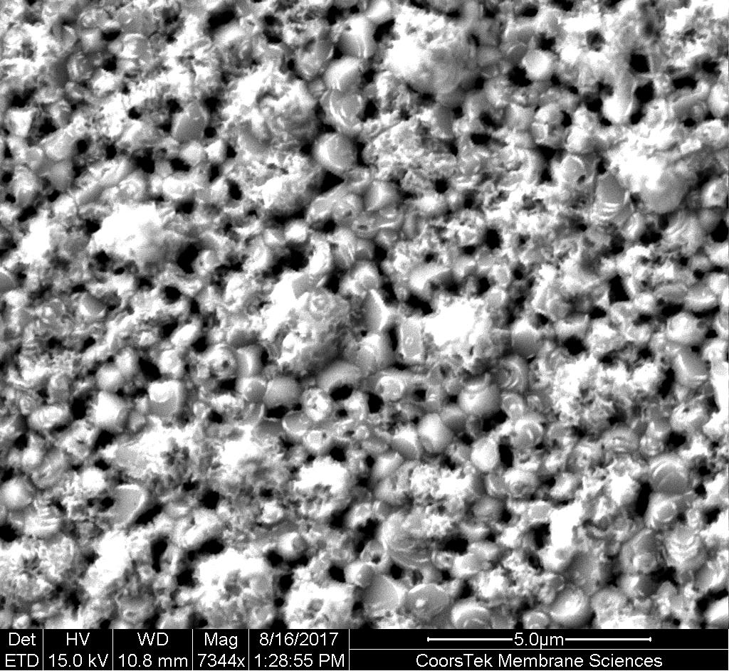
60 5.3.6 SEM Images of the 0, 7 and 20 sccm heat treated samples can be seen in Figure 33, 34 and 35, respectively. Some white looking spots, or lumps, can be seen on the SEM images. These indicate particles lying on top of the surface, i. e. above the rest of the film. The white color result from a charging effect during measurement, which result for low conductivity films. For the 20 sccm films, white looking spots were covering the whole film. However, for the 20 sccm film heated at 1000 C, they were not as white compared to the rest of the surface, which indicate that are merged into the film. For the 0 sccm and 7 sccm samples at all temperatures the white looking particles on top of the surface were only a few, not covering the whole film. This was also the case for the as-deposited films. The images shows that the grain size increase with temperature for all samples, as expected. Also, a large amount of holes, so called pin holes, occur in the films after heat treatment, especially for the films with nonzero N 2 -flow at 900 C and 1000 C. Maybe this is a result of vacancies in the films that diffuses to make bigger holes during heat treatment. If so, the number of vacancies might be larger in the films with a high N 2 -flow due to the escape of nitrogen from the sample. In the following are some detailed observations of each film: 0 sccm, as-deposited: Typical grain length: 0.08µm to 0.25µm. However, as seen from the picture zoomed in, two grains right beside each other is larger, having lengths in the order of the largest grains and widths twice or three times as large. This couple of grains seem to be at a higher level than the surface level, as it has a lighter color. There also is one similarly sized grain, which seems to immersed into the surface. On the first picture of the 0 sccm as-deposited sample white spots can be seen. The biggest is about µm 2, while the smallest are about µm 2. The grains have rounded cylindrical shapes, a bit like rice grains or pills. But maybe they would look more irregular if the resolution was better. There seem to be some holes or cracks between grains, but maybe they are just pit-holes. They are small compared to the grains, and not as clear and circular as the pinholes seen in samples heated at higher temperatures, probably due to their small sizes. 0 sccm, 800 C: The grains are irregularly shaped, not like rounded cylindars, as for the asdeposited sample. Grain size vary a lot: From less than 0.5µm to about 2.7µm. Many of the grains are covered with small dark spots. When zooming in, these spots seem to be clearly defined with roughly shaped edges. There appear three brighter spots on the picture. The whitest and clearest is comparable in size with the smallest grains, being 0.33µm at its widest. The other two appear less bright and more smeared out than the first. They are about 0.5 and 0.75µm at 57

 900 C (e)")


61 (a) as-deposited (b) as-deposited (c) 800 C (d) 900 C (e) 1000 C Figure 33: SEM images of as-deposited and heat treated films of 0 sccm nitrogen flow. 58

 900 C")


62 (a) as-deposited (b) as-deposited (c) 800 C (d) 900 C (e) 900 C (f) 1000 C Figure 34: SEM images of as-deposited and heat treated films of 7 sccm nitrogen flow. 59

 900")


63 (a) as-deposited (b) as-deposited (c) as-deposited (d) 800 C (e) 900 C (f) 1000 C Figure 35: SEM images of as-deposited and heat treated films of 20 sccm nitrogen flow. 60
Fundamentals of X-ray diffraction and scattering
 Fundamentals of X-ray diffraction and scattering Don Savage dsavage@wisc.edu 1231 Engineering Research Building (608) 263-0831 X-ray diffraction and X-ray scattering Involves the elastic scattering of
INGE Engineering Materials. Chapter 3 (cont.)
") Some techniques used: Chapter 3 (cont.) This section will address the question how do we determine the crystal structure of a solid sample? Electron microscopy (by direct and indirect observations) Scanning
Some techniques used: Chapter 3 (cont.) This section will address the question how do we determine the crystal structure of a solid sample? Electron microscopy (by direct and indirect observations) Scanning
Identification of Crystal Structure and Lattice Parameter. for Metal Powders Using X-ray Diffraction. Eman Mousa Alhajji
 Identification of Crystal Structure and Lattice Parameter for Metal Powders Using X-ray Diffraction Eman Mousa Alhajji North Carolina State University Department of Materials Science and Engineering MSE
Growth Of TiO 2 Films By RF Magnetron Sputtering Studies On The Structural And Optical Properties
 Journal of Multidisciplinary Engineering Science and Technology (JMEST) Growth Of TiO 2 Films By RF Magnetron Sputtering Studies On The Structural And Optical Properties Ahmed K. Abbas 1, Mohammed K. Khalaf
ECE440 Nanoelectronics. Lecture 08 Review of Solid State Physics
 ECE440 Nanoelectronics Lecture 08 Review of Solid State Physics A Brief review of Solid State Physics Crystal lattice, reciprocal lattice, symmetry Crystal directions and planes Energy bands, bandgap Direct
Lab IV: Electrical Properties
 Lab IV: Electrical Properties Study Questions 1. How would the electrical conductivity of the following vary with temperature: (a) ionic solids; (b) semiconductors; (c) metals? Briefly explain your answer.
Diffraction Basics. The qualitative basics:
 The qualitative basics: Diffraction Basics Coherent scattering around atomic scattering centers occurs when x-rays interact with material In materials with a crystalline structure, x-rays scattered in
X-ray diffraction
 2.2.3.- X-ray diffraction 2.2.3.1.- Origins and fundamentals of the technique The first experimental evidence concerning x-ray diffraction was given by Max von Laue who in 1912 demonstrated that x-rays
Synthesis and Characterization of DC Magnetron Sputtered ZnO Thin Films Under High Working Pressures
 Accepted Manuscript Synthesis and Characterization of DC Magnetron Sputtered ZnO Thin Films Under High Working Pressures M. Hezam, N. Tabet, A. Mekki PII: S0040-6090(10)00417-7 DOI: doi: 10.1016/j.tsf.2010.03.091
9/28/2013 9:26 PM. Chapter 3. The structure of crystalline solids. Dr. Mohammad Abuhaiba, PE
 Chapter 3 The structure of crystalline solids 1 2 Why study the structure of crystalline solids? Properties of some materials are directly related to their crystal structure. Significant property differences
Lesson 1 X-rays & Diffraction
 Lesson 1 X-rays & Diffraction Nicola Döbelin RMS Foundation, Bettlach, Switzerland February 11 14, 2013, Riga, Latvia Electromagnetic Spectrum X rays: Wavelength λ: 0.01 10 nm Energy: 100 ev 100 kev Interatomic
9/29/2014 8:52 PM. Chapter 3. The structure of crystalline solids. Dr. Mohammad Abuhaiba, PE
 1 Chapter 3 The structure of crystalline solids 2 Home Work Assignments HW 1 2, 7, 12, 17, 22, 29, 34, 39, 44, 48, 53, 58, 63 Due Sunday 12/10/2014 Quiz # 1 will be held on Monday 13/10/2014 at 11:00 am
Atomic Densities. Linear Density Number of atoms per length whose centers lie on the direction vector for a specific crystallographic direction.
 Atomic Densities Linear Density Number of atoms per length whose centers lie on the direction vector for a specific crystallographic direction. Planar Density Number of atoms per unit area that are centered
9/16/ :30 PM. Chapter 3. The structure of crystalline solids. Mohammad Suliman Abuhaiba, Ph.D., PE
 Chapter 3 The structure of crystalline solids 1 Mohammad Suliman Abuhaiba, Ph.D., PE 2 Home Work Assignments HW 1 2, 7, 12, 17, 22, 29, 34, 39, 44, 48, 53, 58, 63 Due Sunday 17/9/2015 3 Why study the structure
X-Ray Diffraction Analysis
 162402 Instrumental Methods of Analysis Unit III X-Ray Diffraction Analysis Dr. M. Subramanian Associate Professor Department of Chemical Engineering Sri Sivasubramaniya Nadar College of Engineering Kalavakkam
LECTURE 7. Dr. Teresa D. Golden University of North Texas Department of Chemistry
 LECTURE 7 Dr. Teresa D. Golden University of North Texas Department of Chemistry Diffraction Methods Powder Method For powders, the crystal is reduced to a very fine powder or microscopic grains. The sample,
An advantage of thin-film silicon solar cells is that they can be deposited on glass substrates and flexible substrates.
 ET3034TUx - 5.2.1 - Thin film silicon PV technology 1 Last week we have discussed the dominant PV technology in the current market, the PV technology based on c-si wafers. Now we will discuss a different
Experiment 2b X-Ray Diffraction* Optical Diffraction Experiments
 * Experiment 2b X-Ray Diffraction* Adapted from Teaching General Chemistry: A Materials Science Companion by A. B. Ellis et al.: ACS, Washington, DC (1993). Introduction Inorganic chemists, physicists,
Lecture C4b Microscopic to Macroscopic, Part 4: X-Ray Diffraction and Crystal Packing
 Lecture C4b Microscopic to Macroscopic, Part 4: X-Ray Diffraction and Crystal Packing X-ray Diffraction Max von Laue won the 1914 Nobel Prize for his discovery of the diffraction of x-rays by crystals.
ECE 440 Lecture 27 : Equilibrium P-N Junctions I Class Outline:
 ECE 440 Lecture 27 : Equilibrium P-N Junctions I Class Outline: Fabrication of p-n junctions Contact Potential Things you should know when you leave Key Questions What are the necessary steps to fabricate
Single crystal X-ray diffraction. Zsolt Kovács
 Single crystal X-ray diffraction Zsolt Kovács based on the Hungarian version of the Laue lab description which was written by Levente Balogh, Jenő Gubicza and Lehel Zsoldos INTRODUCTION X-ray diffraction
This lecture is part of the Basic XRD Course.
 This lecture is part of the Basic XRD Course. Basic XRD Course 1 A perfect polycrystalline sample should contain a large number of crystallites. Ideally, we should always be able to find a set of crystallites
Atomic Densities. Linear Density. Planar Density. Linear Density. Outline: Planar Density
 Atomic Densities Outline: Atomic Densities - Linear Density - Planar Density Single- vs poly- crystalline materials X-ray Diffraction Example Polymorphism and Allotropy Linear Density Number of atoms per
Strain. Two types of stresses: Usually:
 Stress and Texture Strain Two types of stresses: microstresses vary from one grain to another on a microscopic scale. macrostresses stress is uniform over large distances. Usually: macrostrain is uniform
RightCopyright 2006 American Vacuum Soci
 Title Gallium nitride thin films deposite magnetron sputtering Author(s) Maruyama, T; Miyake, H Citation JOURNAL OF VACUUM SCIENCE & (2006), 24(4): 1096-1099 TECHNOL Issue Date 2006 URL http://hdl.handle.net/2433/43541
Metallization deposition and etching. Material mainly taken from Campbell, UCCS
 Metallization deposition and etching Material mainly taken from Campbell, UCCS Application Metallization is back-end processing Metals used are aluminum and copper Mainly involves deposition and etching,
Lecture 12. Physical Vapor Deposition: Evaporation and Sputtering Reading: Chapter 12. ECE Dr. Alan Doolittle
 Lecture 12 Physical Vapor Deposition: Evaporation and Sputtering Reading: Chapter 12 Evaporation and Sputtering (Metalization) Evaporation For all devices, there is a need to go from semiconductor to metal.
Preprint 29th EUPVSEC, September 22-26, 2014, Amsterdam
 EFFECT OF OXYGEN DURING THERMAL ANNEALING ON THE ELECTRICAL AND OPTICAL PROPERTIES OF SPUTTER DEPOSITED AL-DOPED ZNO FILMS FOR HETEROJUNCTION SOLAR CELL APPLICATION Angelika Gorgulla, Nils Brinkmann, Daniel
Silver Diffusion Bonding and Layer Transfer of Lithium Niobate to Silicon
 Chapter 5 Silver Diffusion Bonding and Layer Transfer of Lithium Niobate to Silicon 5.1 Introduction In this chapter, we discuss a method of metallic bonding between two deposited silver layers. A diffusion
CHAPTER 3. Experimental Results of Magnesium oxide (MgO) Thin Films
 Thin Films") CHAPTER 3 Experimental Results of Magnesium oxide (MgO) Thin Films Chapter: III ---------------------------------------------------------------- Experimental Results of Magnesium oxide (MgO) Thin Films
CHAPTER 3 Experimental Results of Magnesium oxide (MgO) Thin Films Chapter: III ---------------------------------------------------------------- Experimental Results of Magnesium oxide (MgO) Thin Films
Characterisation of Zinc Tin Oxide Thin Films Prepared
 Chapter 4 Characterisation of Zinc Tin Oxide Thin Films Prepared by Co-sputtering 4.1 Introduction This chapter describes the preparation of amorphous zinc tin oxide thin films by co-sputtering technique
Influence of Annealing Temperature on the Properties of ITO Films Prepared by Electron Beam Evaporation and Ion-Assisted Deposition
 Kasetsart J. (Nat. Sci.) 42 : 362-366 (2008) Influence of Annealing Temperature on the Properties of ITO Films Prepared by Electron Beam Evaporation and Ion-Assisted Deposition Artorn Pokaipisit 1 *, Mati
High Transmittance Ti doped ITO Transparent Conducting Layer Applying to UV-LED. Y. H. Lin and C. Y. Liu
 High Transmittance Ti doped ITO Transparent Conducting Layer Applying to UV-LED Y. H. Lin and C. Y. Liu Department of Chemical Engineering and Materials Engineering, National Central University, Jhongli,
CHAPTER 4. SYNTHESIS OF ALUMINIUM SELENIDE (Al 2 Se 3 ) NANO PARTICLES, DEPOSITION AND CHARACTERIZATION
 NANO PARTICLES, DEPOSITION AND CHARACTERIZATION") 40 CHAPTER 4 SYNTHESIS OF ALUMINIUM SELENIDE (Al 2 Se 3 ) NANO PARTICLES, DEPOSITION AND CHARACTERIZATION 4.1 INTRODUCTION Aluminium selenide is the chemical compound Al 2 Se 3 and has been used as a precursor
40 CHAPTER 4 SYNTHESIS OF ALUMINIUM SELENIDE (Al 2 Se 3 ) NANO PARTICLES, DEPOSITION AND CHARACTERIZATION 4.1 INTRODUCTION Aluminium selenide is the chemical compound Al 2 Se 3 and has been used as a precursor
Chapter-IV OPTICAL PROPERTIES
 Chapter-IV OPTICAL PROPERTIES 4.1 Ultraviolet/ Visible Spectroscopy UV- visible spectroscopy of wavelength is shorter than visible light, but longer than X- rays. UV-Violet color is the shortest wavelength
Polycrystalline and microcrystalline silicon
 6 Polycrystalline and microcrystalline silicon In this chapter, the material properties of hot-wire deposited microcrystalline silicon are presented. Compared to polycrystalline silicon, microcrystalline
Transmission Electron Microscopy (TEM) Prof.Dr.Figen KAYA
 Prof.Dr.Figen KAYA") Transmission Electron Microscopy (TEM) Prof.Dr.Figen KAYA Transmission Electron Microscope A transmission electron microscope, similar to a transmission light microscope, has the following components along
Transmission Electron Microscopy (TEM) Prof.Dr.Figen KAYA Transmission Electron Microscope A transmission electron microscope, similar to a transmission light microscope, has the following components along
UNIT V -CRYSTAL STRUCTURE
 UNIT V -CRYSTAL STRUCTURE Solids are of two types: Amorphous and crystalline. In amorphous solids, there is no order in the arrangement of their constituent atoms (molecules). Hence no definite structure
CHAPTER 5 Co-DOPED TiO 2 THIN FILMS: RESULTS AND DISCUSSION. 5.1 Introduction. 5.2 Effect of laser energy density (I)
") Chapter 5 Co-doped TiO 2 thin films results and discussion 81 CHAPTER 5 Co-DOPED TiO 2 THIN FILMS: RESULTS AND DISCUSSION 5.1 Introduction Thin films of Co-doped TiO 2 are used in a variety of optoelectronic
Chapter 5 Co-doped TiO 2 thin films results and discussion 81 CHAPTER 5 Co-DOPED TiO 2 THIN FILMS: RESULTS AND DISCUSSION 5.1 Introduction Thin films of Co-doped TiO 2 are used in a variety of optoelectronic
Slide 1. Slide 2. Slide 3. Chapter 19: Electronic Materials. Learning Objectives. Introduction
 Slide 1 Chapter 19: Electronic Materials 19-1 Slide 2 Learning Objectives 1. Ohm s law and electrical conductivity 2. Band structure of solids 3. Conductivity of metals and alloys 4. Semiconductors 5.
Semiconductor Very Basics
 Semiconductor Very Basics Material (mostly) from Semiconductor Devices, Physics & Technology, S.M. Sze, John Wiley & Sons Semiconductor Detectors, H. Spieler (notes) July 3, 2003 Conductors, Semi-Conductors,
Thin Film Characterizations Using XRD The Cases of VO2 and NbTiN
 Thin Film Characterizations Using XRD The Cases of VO2 and NbTiN A thesis submitted in partial fulfillment of the requirement for the degree of Bachelor of Arts / Science in Physics from The College of
The object of this experiment is to test the de Broglie relationship for matter waves,
 Experiment #58 Electron Diffraction References Most first year texts discuss optical diffraction from gratings, Bragg s law for x-rays and electrons and the de Broglie relation. There are many appropriate
Carbon nanostructures. (http://www.mf.mpg.de/de/abteilungen/schuetz/index.php?lang=en&content=researchtopics&type=specific&name=h2storage)
") Carbon nanostructures (http://www.mf.mpg.de/de/abteilungen/schuetz/index.php?lang=en&content=researchtopics&type=specific&name=h2storage) 1 Crystal Structures Crystalline Material: atoms arrange into a
Carbon nanostructures (http://www.mf.mpg.de/de/abteilungen/schuetz/index.php?lang=en&content=researchtopics&type=specific&name=h2storage) 1 Crystal Structures Crystalline Material: atoms arrange into a
Study of The Structural and Optical Properties of Titanium dioxide Thin Films Prepared by RF Magnetron sputtering
 Study of The Structural and Optical Properties of Titanium dioxide Thin Films Prepared by RF Magnetron sputtering Aqeel K. Hadi 1, Muneer H.Jaduaa 1, Abdul- Hussain K. Elttayef 2 1 Wasit University - College
The growth of patterned ceramic thin films from polymer precursor solutions Göbel, Ole
 University of Groningen The growth of patterned ceramic thin films from polymer precursor solutions Göbel, Ole IMPORTANT NOTE: You are advised to consult the publisher's version (publisher's PDF) if you
Engineering 45: Properties of Materials Final Exam May 9, 2012 Name: Student ID number:
 Engineering 45: Properties of Materials Final Exam May 9, 2012 Name: Student ID number: Instructions: Answer all questions and show your work. You will not receive partial credit unless you show your work.
Materials Lab 1(MT344) X-ray Diffractometer Operation and Data Analysis. Instructor: Dr. Xueyan Wu ( 吴雪艳 )
 X-ray Diffractometer Operation and Data Analysis. Instructor: Dr. Xueyan Wu ( 吴雪艳 )") Materials Lab 1(MT344) X-ray Diffractometer Operation and Data Analysis Instructor: Dr. Xueyan Wu ( 吴雪艳 ) Goals To give students a practical introduction into the use of X-ray diffractometer and data collection.
Materials Lab 1(MT344) X-ray Diffractometer Operation and Data Analysis Instructor: Dr. Xueyan Wu ( 吴雪艳 ) Goals To give students a practical introduction into the use of X-ray diffractometer and data collection.
CHAPTER 4: Oxidation. Chapter 4 1. Oxidation of silicon is an important process in VLSI. The typical roles of SiO 2 are:
 Chapter 4 1 CHAPTER 4: Oxidation Oxidation of silicon is an important process in VLSI. The typical roles of SiO 2 are: 1. mask against implant or diffusion of dopant into silicon 2. surface passivation
Hot-wire deposited intrinsic amorphous silicon
 3 Hot-wire deposited intrinsic amorphous silicon With the use of tantalum as filament material, it is possible to decrease the substrate temperature of hot-wire deposited intrinsic amorphous silicon, while
Background Statement for SEMI Draft Document 5945 New Standard: Test Method for Determining Orientation of A Sapphire Single Crystal
 Background Statement for SEMI Draft Document 5945 New Standard: Test Method for Determining Orientation of A Sapphire Single Crystal Notice: This background statement is not part of the balloted item.
Characterization of Materials Using X-Ray Diffraction Powder Diffraction
 Praktikum III, Fall Term 09 Experiment P1/P2; 23.10.2009 Characterization of Materials Using X-Ray Diffraction Powder Diffraction Authors: Michael Schwarzenberger (michschw@student.ethz.ch) Philippe Knüsel
Student Name: ID Number:
 Student Name: ID Number: DEPARTMENT OF MECHANICAL ENGINEERING CONCORDIA UNIVERSITY MATERIALS SCIENCE - MECH 1/ - Sections T & X MIDTERM 003 Instructors: Dr. M.Pugh & Dr. M.Medraj Time Allowed: one (1)
Lecture C4a Microscopic to Macroscopic, Part 4: X-Ray Diffraction and Crystal Packing
 Lecture C4a Microscopic to Macroscopic, Part 4: X-Ray Diffraction and Crystal Packing X-ray Diffraction Max von Laue won the 1914 Nobel Prize for his discovery of the diffraction of x-rays by crystals.
SOLID STATE
 SOLID STATE Short Answer Questions: 1. Derive Bragg s equation? Ans. Bragg s equation: W.H. Bragg has proposed an equation to explain the relation between inter planar distance (d) and wave length ( λ
PHYSICAL ELECTRONICS(ECE3540) Brook Abegaz, Tennessee Technological University, Fall 2013
 Brook Abegaz, Tennessee Technological University, Fall 2013") PHYSICAL ELECTRONICS(ECE3540) Brook Abegaz, Tennessee Technological University, Fall 2013 1 Chapter 1 The Crystal Structure of Solids Physical Electronics: Includes aspects of the physics of electron movement
PHYSICAL ELECTRONICS(ECE3540) Brook Abegaz, Tennessee Technological University, Fall 2013 1 Chapter 1 The Crystal Structure of Solids Physical Electronics: Includes aspects of the physics of electron movement
E45 Midterm 01 Fall 2007! By the 0.2% offset method (shown on plot), YS = 500 MPa
, YS = 500 MPa") 1.!Mechanical Properties (20 points) Refer to the following stress-strain plot derived from a standard uniaxial tensile test of a high performance titanium alloy to answer the following questions. Show
1.!Mechanical Properties (20 points) Refer to the following stress-strain plot derived from a standard uniaxial tensile test of a high performance titanium alloy to answer the following questions. Show
High Resolution X-ray Diffraction
 High Resolution X-ray Diffraction Nina Heinig with data from Dr. Zhihao Donovan Chen, Panalytical and slides from Colorado State University Outline Watlab s new tool: Panalytical MRD system Techniques:
GEOLOGY 333 LAB 14. Lab Final Exam See information sheet for details
 GEOLOGY 333 LAB 14 X-RAY DIFFRACTION OF EVERYDAY MATERIALS Lab Final Exam See information sheet for details! Next week during Lab (10 am - noon, May 2, 69 CAB).! 25% of Lab grade, out of 65 points plus
Fabrication Technology
 Fabrication Technology By B.G.Balagangadhar Department of Electronics and Communication Ghousia College of Engineering, Ramanagaram 1 OUTLINE Introduction Why Silicon The purity of Silicon Czochralski
much research (in physics, chemistry, material science, etc.) have been done to understand the difference in materials properties.
 have been done to understand the difference in materials properties.") 1.1: Introduction Material science and engineering Classify common features of structure and properties of different materials in a well-known manner (chemical or biological): * bonding in solids are classified
1.1: Introduction Material science and engineering Classify common features of structure and properties of different materials in a well-known manner (chemical or biological): * bonding in solids are classified
Chapter 3 Basic Crystallography and Electron Diffraction from Crystals. Lecture 9. Chapter 3 CHEM Fall, L. Ma
 Chapter 3 Basic Crystallography and Electron Diffraction from Crystals Lecture 9 Outline The geometry of electron diffraction Crystallography Kinetic Theory of Electron diffraction Diffraction from crystals
Crystalline Silicon Solar Cells
 12 Crystalline Silicon Solar Cells As we already discussed in Chapter 6, most semiconductor materials have a crystalline lattice structure. As a starting point for our discussion on crystalline silicon
Physics 6180: Graduate Physics Laboratory. Experiment CM5: X-ray diffraction and crystal structures
 Physics 6180: Graduate Physics Laboratory Experiment CM5: X-ray diffraction and crystal structures References: Preston and Dietz, Expt. 10 pp. 180-197 Eisberg and Resnick, Quantum Physics, Sec. 9 Kittel,
Halbleiter Prof. Yong Lei Prof. Thomas Hannappel
 Halbleiter Prof. Yong Lei Prof. Thomas Hannappel yong.lei@tu-ilmenau.de thomas.hannappel@tu-ilmenau.de http://www.tu-ilmenau.de/nanostruk/ Solid State Structure of Semiconductor Semiconductor manufacturing
ECE 541/ME 541 Microelectronic Fabrication Techniques
 ECE 541/ME 541 Microelectronic Fabrication Techniques MW 4:00-5:15 pm Metrology and Characterization Zheng Yang ERF 3017, email: yangzhen@uic.edu ECE541/ME541 Microelectronic Fabrication Techniques Page
Materials Synthesis Via Directed Vapor Deposition
 Chapter 6 Materials Synthesis Via Directed Vapor Deposition 6.1 Overview Experimental work was undertaken to explore the ability of Directed Vapor Deposition to synthesize a variety of films in a low vacuum
It is instructive however for you to do a simple structure by hand. Rocksalt Structure. Quite common in nature. KCl, NaCl, MgO
 Today the structure determinations etc are all computer -assisted It is instructive however for you to do a simple structure by hand Rocksalt Structure Quite common in nature KCl, NaCl, MgO 9-1 Typical
CHAPTER 5. DEPOSITION AND CHARACTERIZATION OF ZINC STANNATE (Zn 2 SnO 4 ) THIN FILMS
 THIN FILMS") 106 CHAPTER 5 DEPOSITION AND CHARACTERIZATION OF ZINC STANNATE (Zn 2 SnO 4 ) THIN FILMS 5.1 INTRODUCTION Post-transition-metal oxides and their alloys have unique physical properties. Despite their large
106 CHAPTER 5 DEPOSITION AND CHARACTERIZATION OF ZINC STANNATE (Zn 2 SnO 4 ) THIN FILMS 5.1 INTRODUCTION Post-transition-metal oxides and their alloys have unique physical properties. Despite their large
CHAPTER 8: Diffusion. Chapter 8
 1 CHAPTER 8: Diffusion Diffusion and ion implantation are the two key processes to introduce a controlled amount of dopants into semiconductors and to alter the conductivity type. Figure 8.1 compares these
The Science and Engineering of Materials, 4 th ed Donald R. Askeland Pradeep P. Phulé. Chapter 3 Atomic and Ionic Arrangements
 The Science and Engineering of Materials, 4 th ed Donald R. Askeland Pradeep P. Phulé Chapter 3 Atomic and Ionic Arrangements 1 Objectives of Chapter 3 To learn classification of materials based on atomic/ionic
Optical parameter determination of ZrO 2 thin films prepared by sol gel dip coating
 International Journal of ChemTech Research CODEN (USA): IJCRGG ISSN : 0974-490 Vol.6, No.13, pp 534-5346, November 014 MESCon 014 [4th -5 th September 014] National Conference on Material for Energy Storage
416 Solid State Physics ; Introduction & Overview
 416 Solid State Physics 8-29-2016; Introduction & Overview Assignment: Read chapter 1 of Kittel for next time on crystal symmetries. This course covers concepts in solid state physics. Note that physics-related
THE INFLUENCE OF NITROGEN CONTENT ON THE MECHANICAL PROPERTIES OF TiN x THIN FILMS PREPARED BY REACTIVE MAGNETRON SPUTTERING
 Bulletin of the Transilvania University of Braşov Series I: Engineering Sciences Vol. 5 (54) No. 2-2012 THE INFLUENCE OF NITROGEN CONTENT ON THE MECHANICAL PROPERTIES OF TiN x THIN FILMS PREPARED BY REACTIVE
Instrument Configuration for Powder Diffraction
 Instrument Configuration for Powder Diffraction Advanced X-ray Workshop S.N. Bose National Centre for Basic Sciences, 14-15/12/2011 Innovation with Integrity Overview What is the application? What are
Microstructural Characterization of Materials
 Microstructural Characterization of Materials 2nd Edition DAVID BRANDON AND WAYNE D. KAPLAN Technion, Israel Institute of Technology, Israel John Wiley & Sons, Ltd Contents Preface to the Second Edition
Previous Lecture. Vacuum & Plasma systems for. Dry etching
 Previous Lecture Vacuum & Plasma systems for Dry etching Lecture 9: Evaporation & sputtering Objectives From this evaporation lecture you will learn: Evaporator system layout & parts Vapor pressure Crucible
Supporting Information. Solution-Processed 2D PbS Nanoplates with Residual Cu 2 S. Exhibiting Low Resistivity and High Infrared Responsivity
 Supporting Information Solution-Processed 2D PbS Nanoplates with Residual Cu 2 S Exhibiting Low Resistivity and High Infrared Responsivity Wen-Ya Wu, Sabyasachi Chakrabortty, Asim Guchhait, Gloria Yan
Influence of In/Sn ratio on nanocrystalline indium tin oxide thin films by spray pyrolysis method
 Available online at www.scholarsresearchlibrary.com Scholars Research Library Archives of Physics Research, 2011, 2 (1): 19-25 (http://scholarsresearchlibrary.com/archive.html) ISSN 0976-0970 CODEN (USA):
PHYSICSOF SOLARCELLS. Jenny Nelson. Imperial College, UK. Imperial College Press ICP
 im- PHYSICSOF SOLARCELLS Jenny Nelson Imperial College, UK ICP Imperial College Press Contents Preface v Chapter 1 Introduction 1 1.1. Photons In, Electrons Out: The Photovoltaic Effect 1 1.2. Brief History
X-RAY DIFFRACTION. X- Ray Sources Diffraction: Bragg s Law Crystal Structure Determination
 X-RAY DIFFRACTION X- Ray Sources Diffraction: Bragg s Law Crystal Structure Determination Part of MATERIALS SCIENCE & ENGINEERING A Learner s Guide AN INTRODUCTORY E-BOOK Anandh Subramaniam & Kantesh Balani
ATTACHMENTES FOR APD 2000 PRO POWDER X-RAY DIFFRACTOMETER. Monochromators
 Monochromators Secondary graphite monochromator Johansson Ka 1 monochromator Parabolic monochromator Secondary flat and curved graphite monochromators suitable for Ag, Cr, Fe, Cu, Co and Mo radiations
The next thin-film PV technology we will discuss today is based on CIGS.
 ET3034TUx - 5.3 - CIGS PV Technology The next thin-film PV technology we will discuss today is based on CIGS. CIGS stands for copper indium gallium selenide sulfide. The typical CIGS alloys are heterogeneous
X-RAY DIFFRACTION IN SEMICONDUCTOR INDUSTRY AND RESEARCH
 X-RAY DIFFRACTION IN SEMICONDUCTOR INDUSTRY AND RESEARCH M. Leszczyński High Pressure Research Center UNIPRESS, Sokolowska 29/37, 01 142 Warsaw, Poland, e-mail: mike@unipress.waw.pl ABSTRACT The paper
Microstructure of Electronic Materials. Amorphous materials. Single-Crystal Material. Professor N Cheung, U.C. Berkeley
 Microstructure of Electronic Materials Amorphous materials Single-Crystal Material 1 The Si Atom The Si Crystal diamond structure High-performance semiconductor devices require defect-free crystals 2 Crystallographic
Influence of Heat Treating for ZnS:Mn Sputtering Targets on Inorganic Electroluminescent Device Active Layer Films
 Mem. Fac. Eng., Osaka City Univ., Yol. 49, pp. ]-5 (2008) Influence of Heat Treating for ZnS:Mn Sputtering Targets on Inorganic Electroluminescent Device Active Layer Films Ryuta TANAKA*,Ikuko SAKAI**,Kenji
Properties of Inclined Silicon Carbide Thin Films Deposited by Vacuum Thermal Evaporation
 182 Properties of Inclined Silicon Carbide Thin Films Deposited by Vacuum Thermal Evaporation Oday A. Hamadi, Khaled Z. Yahia, and Oday N. S. Jassim Abstract In this work, thermal evaporation system was
1. Introduction. What is implantation? Advantages
 Ion implantation Contents 1. Introduction 2. Ion range 3. implantation profiles 4. ion channeling 5. ion implantation-induced damage 6. annealing behavior of the damage 7. process consideration 8. comparison
Travaux Pratiques de Matériaux de Construction
 Travaux Pratiques de Matériaux de Construction Section Matériaux 6 ème semestre 2009 Etude de Matériaux Cimentaire Par Diffraction des Rayons X Responsable: Silke Ruffing E-Mail: silke.ruffing@epfl.ch
LECTURE 8. Dr. Teresa D. Golden University of North Texas Department of Chemistry
 LECTURE 8 Dr. Teresa D. Golden University of North Texas Department of Chemistry Practical applications for lattice parameter measurements: -determine composition (stoichiometry) of the sample -determine
Thin Film Scattering: Epitaxial Layers
 Thin Film Scattering: Epitaxial Layers 6th Annual SSRL Workshop on Synchrotron X-ray Scattering Techniques in Materials and Environmental Sciences: Theory and Application May 29-31, 2012 Thin films. Epitaxial
Advanced Methods for Materials Research. Materials Structure Investigations Materials Properties Investigations
 Advanced Methods for Materials Research Materials Structure Investigations Materials Properties Investigations Advanced Methods for Materials Research 1. The structure and property of sample and methods
Physical Vapor Deposition (PVD) Zheng Yang
 Zheng Yang") Physical Vapor Deposition (PVD) Zheng Yang ERF 3017, email: yangzhen@uic.edu Page 1 Major Fabrication Steps in MOS Process Flow UV light Mask oxygen Silicon dioxide photoresist exposed photoresist oxide
Physical Vapor Deposition (PVD) Zheng Yang ERF 3017, email: yangzhen@uic.edu Page 1 Major Fabrication Steps in MOS Process Flow UV light Mask oxygen Silicon dioxide photoresist exposed photoresist oxide
Microelettronica. Planar Technology for Silicon Integrated Circuits Fabrication. 26/02/2017 A. Neviani - Microelettronica
 Microelettronica Planar Technology for Silicon Integrated Circuits Fabrication 26/02/2017 A. Neviani - Microelettronica Introduction Simplified crosssection of an nmosfet and a pmosfet Simplified crosssection
FABRICATION ENGINEERING MICRO- NANOSCALE ATTHE AND. Fourth Edition STEPHEN A. CAMPBELL. of Minnesota. University OXFORD UNIVERSITY PRESS
 AND FABRICATION ENGINEERING ATTHE MICRO- NANOSCALE Fourth Edition STEPHEN A. CAMPBELL University of Minnesota New York Oxford OXFORD UNIVERSITY PRESS CONTENTS Preface xiii prrt i OVERVIEW AND MATERIALS
Structural and Optical Properties of MnO 2 : Pb Nanocrystalline Thin Films Deposited By Chemical Spray Pyrolysis
 IOSR Journal of Engineering (IOSRJEN) e-issn: 2250-3021, p-issn: 2278-8719 Vol. 3, Issue 4 (April. 2013), V4 PP 52-57 Structural and Optical Properties of MnO 2 : Pb Nanocrystalline Thin Films Deposited
Most semiconductor devices contain at least one junction between p-type and n-type material. These p-n junctions are fundamental to the performance
 Ch. 5: p-n Junction Most semiconductor devices contain at least one junction between p-type and n-type material. These p-n junctions are fundamental to the performance of functions such as rectification,