A newsletter from the Facilitation Centre for Industrial Plasma Technologies Institute for Plasma Research. Issue 64 September December 2011.
|
|
|
- Hilary Barber
- 6 years ago
- Views:
Transcription

1 A newsletter from the Facilitation Centre for Industrial Plasma Technologies Institute for Plasma Research Issue 64 September December 2011 Editor's Note About FCIPT Contents Path towards the Development of Multi-Layer Thin Films for Photovoltaic Applications Deposition and Characterization of Dielectric Films by PECVD Method Development of Tube Based RF Power Supply with Matching Network Other News
2 Editor s Note Solar energy is an affordable, in-exhaustible, and clean source of energy. This energy can be harnessed as long the Sun shines upon us. Solar energy can be converted into electrical energy through photovoltaic technology. Many types of absorber layers/materials, to form the solar cells, have been developed over a period of time. However, most of these materials are either cost intensive, scarce, or hazardous. Hence, efforts are on, all over the world, to develop new absorber materials which are affordable, abundant and non-hazardous; even if the efficiencies are low to start with. CZTS is one of such absorber materials and an efficiency of 19% (max. on lab scale samples) was already achieved. A program to develop CZTS based solar cells is being initiated at FCIPT and Mr. Sagar Agrawal has explained in detail. Editor : Dr. S. Mukherjee Co-Editor : A. Satyaprasad Conference Presentations from FCIPT 2 PLASMA PROCESSING UPDATE

3 About FCIPT Facilitation Centre for Industrial Plasma Technologies The Institute for Plasma Research (IPR) is exclusively devoted to research in plasma science, technology and applications. It has a broad charter to carry out experimental and theoretical research in plasma sciences with emphasis on the physics of magnetically confined plasmas and certain aspects of nonlinear phenomena. The institute also has a mandate to stimulate plasma research activities in the universities and to develop plasma-based technologies for the industries. It also contributes to the training of plasma physicists and technologists in the country. IPR has been declared as the domestic agency responsible in INDIA to design, build and deliver advanced systems to ITER (International Thermonuclear Experimental Reactor), to develop nuclear fusion as a viable long-term energy option. The Facilitation Centre for Industrial Plasma Technologies (FCIPT) links IPR with the Indian industries and commercially exploits its knowledgebase. FCIPT interacts closely with entrepreneurs through the phases of feasibility study, incubation, development, demonstration and delivery of technologies. Complete package of a broad spectrum of plasma-based industrial technologies and facilitation services is offered. Some of the important areas in which FCIPT has worked or has been working on, include Plasma Surface Engineering, Plasma Pyrolysis/ Gasification/ Energy recovery, Plasma Diagnostics, Plasma based Nano Patterning and Nano Synthesis, Plasma based Thin film Deposition, Plasma Material Interaction, Plasma based High Heat-flux Source Development, Space Plasma and Stealth technologies, Textile Engineering, Solar Cell Development etc. The Centre has process development laboratories, jobshops and advanced material characterisation facilities like Scanning Electron Microscope, X-ray Diffractometer, Microhardness testing facilities, which are open to users from industry, research establishments and universities. For further information, please visit our website. This newsletter is designed to update the readers with the latest developments in the important field of plasma processing and plasma based technology development, and to look for new industrial opportunities. We would be very happy to have you write to us on ways of improving this service. Please visit our website: or Path towards the Development of M u ltilayer T h in Fi lms f o r Photovoltaic Application Sagar Agrawal Photovoltaic (Solar Cell) is the technology that converts solar power in to electrical power. As long as sun light is shining on the solar cell, it generates electrical power and when the light stops, the electricity stops. Solar cells are made of materials called semiconductors, which have weakly bonded electrons occupying a band of energy called the valence band. When energy exceeding a certain threshold, called the band gap energy, is applied to a valence electron, the bond is broken and the electron is somewhat free to move around in a new energy band called the conduction band where it can conduct electricity through the material. Thus, the free electrons in the conduction band are separated from the valence band by the band gap (measured in units of electron volts or ev). This energy needed to free the electrons can be supplied by photons (or in simple language - light). There, a specially made selective contact that collects conduction band electrons, drive such electrons to the external circuit. Silicon (Si), one of the most abundant materials in the Earth's crust, is the semiconductor used in crystalline form (c-si) for 90% of the photo voltaic (PV) applications today. Although c-si is well established for PV applications, there is an intense need to develop a totally different semiconductor technology to achieve lower cost and improved manufacturability at larger scales than that could be envisioned for Si wafer-based modules. The main problem with the c-si based PVs is that c-si wafers are expensive and slow to grow and c-si requires the greatest thickness (~300µm) to absorb sunlight, among all the other absorbing semiconductors due to its unique optical properties. Overall goal of the PV research is to reduce the manufacturing cost (use less semiconductor material by making thinner solar cells, use less expensive PLASMA PROCESSING UPDATE 3

 receive most of the 4 2 attention.")
, Copper Indium Gallium Diselenide (CuInGaSe, also known as 2 CIGS), and Copper Indium Disulphide")
 and high optical absorption coefficient 4-1 (typically of the order of 5x10 cm ). Typical structure and thickness of this kind of solar cell is shown in the fig.")

4 semiconductor materials and increase the material utilization by reducing the wastage of material in semiconductor and cell fabrication) and improve the performance. Thus, it is recognized that other semiconductors are better suited to absorb the solar energy spectrum. These other materials are in development or initial commercialization today. Some are called thin film semiconductors, of which amorphous silicon (a-si), copper Indian gallium diselenide or disulfide (Cu (In Ga )(Se,S) 2 x 1-x 2 or CIGS), cadmium telluride (CdTe) and recently copper zinc tin sulfide (Cu ZnSnS or CZTS) receive most of the 4 2 attention. When they are fabricated into useful devices, they are so thin that they must be deposited on a foreign material called a substrate like glass, thin metallic foil for mechanical support. Of late, study on the development of low cost thin film solar cells based on Cadmium Telluride (CdTe), Copper Indium Gallium Diselenide (CuInGaSe, also known as 2 CIGS), and Copper Indium Disulphide (CuInS, also known 2 as CIS) have attracted much attention and a lot of work has been carried out. These solar cells have shown higher conversion efficiencies (16.7%, 19.5%, and 11.4% respectively) and high optical absorption coefficient 4-1 (typically of the order of 5x10 cm ). Typical structure and thickness of this kind of solar cell is shown in the fig.1, which is a multilayer thin film device. All the layers are deposited on glass. Bottom-most layer is a back contact layer which is a conductive metallic layer, which acts as one electrode of the device. Above this layer there is an absorbing layer, which is made of semiconductor material to absorbs the sunlight and produce the charge particles. Above this layer there is a buffer layer, which forms a pn-junction with the previous layer and helps to reduce the recombination of the opposite charge particles and thus enhances the separation of charge particles, hence the efficiency. Top-most layer is the transparent conducting oxide (TCO) layer, which is highly transparent for the visible spectrum in sun light to allow the sunlight to reach the absorbing layer and is conducting in nature to work as the other electrode of the device. There are various choices of materials as shown in figure 1 for different layers. Fig.1: Typical Structure of Multilayer Thin Film Compound Solar Cell. However, these absorber coatings have certain limitations too. In the case of CIGS coatings, the scarcity of the rare element Indium (In) is the major shortcoming. On the basis of abundance of Indium in the earth crust (0.049 ppm only) and current consumption rates, it is estimated that Indium reserves will get exhausted in a short time period of only thirteen years. In the case of Cadmium based absorber coatings such as CdTe, the important drawbacks are concerned with the toxic nature of Cadmium, and the extremely short abundance of the Tellurium. Therefore, the disposal and long term safety of CdTe is a known issue in the large-scale commercialization of CdTe solar panels. Hence, there is a great necessity for the development of thin film absorber coatings, free from Indium and Cadmium. Copper Zinc Tin Sulfide (CZTS) is one of the promising materials as an absorber layer in thin film solar cells because of its excellent material properties. It has a direct band gap of ~1.45eV, which is very close to the optimum band gap of the semiconductors used for PV solar energy conversion and 4-1 has a high absorption coefficient (10 cm ). Various research groups all over the world are working on this new material and demonstrated up to 9.7% efficiency, which proves the great potential of this material to develop a commercial technology for the solar energy in future. FCIPT has also started an activity with the ultimate aim to develop a multilayer thin film solar cell device using Physical Vapour Deposition (PVD) technique. In the initial 4 PLASMA PROCESSING UPDATE
 has been studied and further experiments are going on.")


5 phase of the activity, bottom most layer of Molybdenum (Mo) back contact and the top most layer of TCO (ZnO:Al) has been studied and further experiments are going on. We have deposited the Mo thin film on soda lime glass using DC magnetron sputtering technique and achieved a low -5 resistive (ρ~3x10? -cm) and adherent to glass ~500nm thin film of Mo, which is suitable to use as a back contact electrode for the thin film solar cell. Figure 2 shows the SEM images of cross section and surface of the film. Figure 3 shows XRD results, which indicate that film is polycrystalline and Mo is formed in bcc phase. Cross Section Surface ~300nm Mo Glass ~300nm M = 25K M = 50K Fig. 2: SEM Images of the Mo Thin Film deposited on glass We have also deposited Aluminum doped Zinc oxide (ZnO:Al) thin film on glass using DC magnetron sputtering with pure Zinc and Aluminum targets in a gas environment of Argon and Oxygen. We have achieved ~1µm thin film with more than 80% transparency in visible range and 1? - cm resistivity with 4% Al doping. Further experiments are going on to achieve the lower resistivity. Figure 4 shows the SEM cross section and surface images of the film. Figure 5 shows the film deposited on glass (red circle), which is transparent as the letters beneath the glass are clearly visible. Fig.3: XRD results of Mo on glass thin Film PLASMA PROCESSING UPDATE 5


6 Surface Cross Section ~ 1µm ZnO:Al ~ 1µm M = 25K Glass M = 25K Fig. 4: SEM Images of the ZnO:Al thin film deposited on glass Fig.5: Transparent ZnO:Al thin film However, all the layers have to be studied individually and then the complete multilayer thin film solar cell has to be developed. However, these are the preliminary results and a detailed study is underway. Deposition & Characterization of Dielectric Films by PECVD Method Purvi Kikani Polymer films deposited by PECVD method are widely used in dielectric and photonic applications such as high/low k films for dielectric devices, high performance capacitors, AR coatings, band gap filters, wave guides etc. The k of a material is defined as the ratio of material's permittivity to the permittivity of vacuum. It is a measure of the relative amount of polarization induced by an electric field applied. A low k dielectric is a dielectric that has low ability to polarize and hold charge. Low k dielectrics are good insulators for isolating signal carrying conductors from each other. Thus low k dielectrics are a necessity in very dense multilayered ICs wherein coupling between very close metal lines need to be suppressed to prevent degradation in dielectric performance. A high k dielectric on the other hand has high permittivity. Because high k dielectrics are good at holding charges, they are preferred dielectrics for capacitors. They are also used in memory cells that store digital data in the form of charge [1]. Polymer materials such as fluorocarbon, polyamide, Siloxane, Silazane, hydrocarbons, silicon dioxide, silicon nitride, silicon oxy nitride etc. are promising candidates for their use in microelectronic applications as a dielectric material [1, 2, 3, 4, 5, 6]. Dielectric films can be deposited by various methods such as Physical Vapour Deposition (PVD), Chemical Vapour Deposition (CVD) and by Plasma Enhanced Chemical Vapour Deposition (PECVD). In CVD, the deposition of the film and its properties are controlled by the temperature of the substrate and the deposition process takes place under thermodynamic equilibrium and the film has a well-defined structure and is usually crystalline (single crystal or polycrystalline). In contrast to CVD, the PECVD method is a nonequilibrium technique, where the process is controlled mainly by the energy of the electrons in the plasma. As a result, the plasma dissociates the molecules in the gas phase into a variety of radicals, which recombine on the substrate to form a solid film comprising a variety of different bonds. The films deposited by PECVD are usually amorphous materials. The substrate temperature may affect the properties of the deposited film, but it is typically lower than the temperature that is required for depositing a film from the gas phase by thermal CVD. Recently, considerable work has been undertaken to fabricate polymeric dielectric and photonic thin films using PECVD techniques due to its room temperature, solvent free and versatile operation. Many organic precursors can be 6 PLASMA PROCESSING UPDATE
 films, exhibiting highly cross linked structures have been targeted for optical and dielectric applications such as waveguides, anti-reflection coatings, and band gap filters")
![for integrated optics, high performance capacitors and dielectric devices [1].](/docs-images/76/74075911/images/7-10.jpg "Siloxane based films prepared by Plasma Enhanced Chemical Vapor Deposition (PECVD) consist of Si-O-Si and Si-CH 3 bonds that are chemically stable, resist thermal decomposition and feature low")
![moisture absorption. These films have been widely used in variety of industries [7].](/docs-images/76/74075911/images/7-11.jpg "In the present work we have deposited plasma polymer dielectric film using Hexamethyldisiloxane (HMDSO) and Oxygen gas mixture at different ratios by PECVD method on metal substrate.")
 power source at a frequency of 13.56 MHz.")

7 selected to prepare thin polymer films with a wide range of compositions and chemical functionalities. Plasma polymerized (PP-) films, exhibiting highly cross linked structures have been targeted for optical and dielectric applications such as waveguides, anti-reflection coatings, and band gap filters for integrated optics, high performance capacitors and dielectric devices [1]. Siloxane based films prepared by Plasma Enhanced Chemical Vapor Deposition (PECVD) consist of Si-O-Si and Si-CH 3 bonds that are chemically stable, resist thermal decomposition and feature low moisture absorption. These films have been widely used in variety of industries [7]. In the present work we have deposited plasma polymer dielectric film using Hexamethyldisiloxane (HMDSO) and Oxygen gas mixture at different ratios by PECVD method on metal substrate. In this study, a-sioxcyh z films were deposited in a cylindrical stainless steel process chamber having dimensions of 60 cm diameter and 30 cm height. Plasma was generated by Radio Frequency (RF) power source at a frequency of MHz. Silicon wafers, polished Aluminum round samples, and polyethylene sheets were used as substrates for deposition in a parallel plate configuration. Gas mixture was introduced via shower-head cum top electrode for uniform gas distribution. Schematic of the system used is shown in figure 1. Fig. 2: Oxygen % vs. Contact Angle FTIR results also confirmed the presence of hydrocarbon species at 0% Oxygen, their gradual reduction with increasing oxygen concentration in the gas mixture, and very minimal at 90 % Oxygen as shown in figure 3 (a) and figure 3 (b) respectively. Fig. 1: Schematic of PECVD Deposition System Film was deposited at a constant operating pressure of 0.1 mbar with variable oxygen concentration from % in the gas mixture. Deposited films were tested for wettability and surface chemistry by means of Contact Angle Goniometer and Fourier Transform Infra-Red (FTIR) Spectroscopy respectively. It was found that the wettability increases with increased oxygen content in the gas mixture as shown in the figure 2 below. Fig. 3(a): FTIR Spectra at 0 % Oxygen PLASMA PROCESSING UPDATE 7
: MIM Structure Fig.")
: C-V Plot at 10 KHz Fig.")
8 Fig. 3(b): FTIR Spectra at 90 % Oxygen Fig. 4(a): MIM Structure Fig. 4(b): MIS Structure Fig. 5(a): C-V Plot at 10 KHz Fig. 5(b): C-V Plot at 1 MHz 8 PLASMA PROCESSING UPDATE

9 In order to measure the dielectric constant of the deposited films, Metal-Insulator-Metal (MIM) and Metal-Insulator- Semiconductor (MIS) sandwich structures were fabricated as shown in figure 4a and 4b respectively. Top metal contacts for MIM and MIS structures were deposited using thermal evaporation method. Capacitance- Voltage (C-V) characteristics were measured for MIS structure at 10 KHz and 1 MHz frequency as shown in figure 5 (a) and 5 (b) respectively. We can see that the capacitance of dielectric film reduces with increasing frequency. This describes poor dielectric properties of deposited material at high operating frequencies. This generally happens due to high concentration of free radicals in the film. These radicals react with oxygen and form polar groups. Dielectric constant calculated for low and high frequency is 1.5 and 0.21 respectively for deposited film. References [1] Thin Solid Films 515 (2007) [2] Thin Solid Films 515 (2007) [3] Surface & Coating Technologies (2003) [4] Micro Electronics Journal 35 (2004) [5] Materials Science in Semiconductor Processing 7 (2004) [6] Thin Solid Films 83 (1981) [7] Materials Science in Semiconductor Processing 5 (2003) Development of Tube based RF Power Supply with Matching Network Vishal Jain Institute for Plasma Research (IPR) has vast knowledge and expertise in developing radio frequency (RF) power supplies of high power rating. At Facilitation Centre for Plasma Technologies (FCIPT), with the technical inputs from IPR, a tube based RF power supply was developed for operating on plasma loads for various industrial applications. The power supply comprises of a high voltage full bridge converter system for supplying 5 kv DC to anode of the tube, a Hartley oscillator based tank circuit to provide a high frequency signal input to the grid of the tube, a heating system for cathode heating at 20A and 6V, filter system for filtering low frequency and high frequency signals using low pass and high pass filters respectively at appropriate place in the circuit, measuring and controlling system etc. The mode of operation was chosen to be as class AB amplification for which the grid was kept at slightly negative voltage. RF supply up to 1kW power is very much suitable for applications like plasma enhanced chemical vapour deposition (PECVD), plasma based physical vapour deposition (PVD) etc. Hence, the RF supply of 600W, MHz was developed at FCIPT, to test its suitability for plasma applications, along with the suitable matching network. Figure 1 shows the basic topology of the RF power supply including DC supply, tank circuit, tube etc. and also shows the Hartley oscillator circuit which is essentially a configuration that uses two series-connected coils and a single capacitor to comprise a tank. In the Hartley oscillator the tuned LC circuit is connected between the plate and grid of the triode. The advantages of the Hartley Oscillator are: (1) The frequency may be varied using a variable capacitor (2) The output amplitude remains constant over a frequency range (3) Either a tapped coil or two fixed inductors are needed PLASMA PROCESSING UPDATE 9


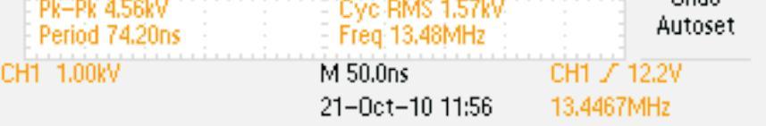
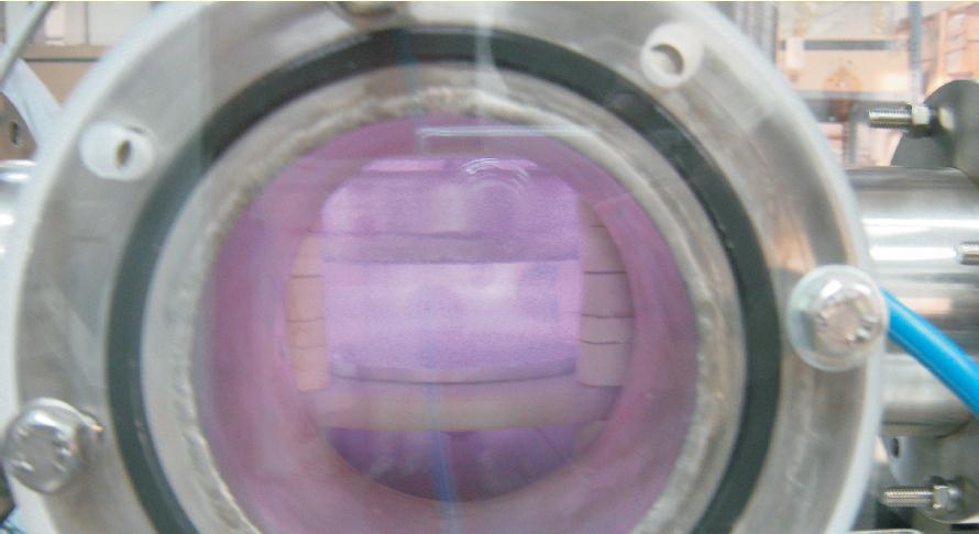
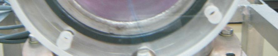
10 Fig. 4: Magnetron RF plasma Fig. 1: Basic topology of the RF source Fig. 2: RF output Wave-form Fig. 3: Capacitively coupled RF PECVD Plasma 10 PLASMA PROCESSING UPDATE

11 Figure 2 shows the RF output voltage waveform across 50 Ohm resistive load and the power supply has been successfully tested with plasma load as well. Figure 3 shows the photograph of the capacitively coupled plasma load and figure 4 shows the photograph of a magnetron plasma load operating with a RF power source. Development of Matching Network The plasma load is a complex load and hence, in order to draw maximum power from the source for better efficiency, the load and source should be coupled through a network which compensates the reactive part of the load. This ensures that the voltage and current are in phase with each other depicting a resistive load. Such networks are known as matching networks. To design a matching network, knowledge of complex load parameters is essential. A lot of literature is available suggesting on how to find the complex impedance of the plasma load under certain operating conditions. We designed the matching network for a magnetron which has 100 gauss permanent magnetic field. For this kind of plasma, the load parameters were selected from the literature and then we identified the suitable network, which is L type network, and we also ensured that the Thevnin's impedance across the load is a complex conjugate of the plasma load impedance. We also validated the network parameters by using an equivalent component across the plasma load and observed that the net power transferred to the plasma is increased. We observed an L type network with an inductor of 0.7 to 0.9 micro Henry and a capacitor of 500 to 3000 Pico Farad, can suitably increase the net power transferred to the plasma load. The advantage of a tube based power supply is its ability to withstand high power, which is the sole limitation of solid state techniques for RF power generation. Plasma Torch Activities Dr. G. Ravi Since thermal plasmas are of great technological interest, industrial thermal plasma systems are in use in variety of applications ranging from plasma spraying & waste treatment, to metal melting, smelting, & spacecraft re-entry simulation. Facilitation Center for Industrial Plasma Technologies (FCIPT) has been involved in developing many thermal plasma technologies for over a decade. Graphite electrode based torches have been used successfully for pyrolysis of medical and plastic waste, involving thermal disintegration of carbonaceous material in the absence of oxygen. Non-expendable electrode based torches have also been developed and used in variety of applications e.g. spherodization of irregular alumina, dissociation of Zircon sand etc. A new program for development of high power (100 - several 100's of kw) nontransferred plasma torches for use as high heat flux sources has now been initiated, keeping in mind several high-end applications such as fusion, metallurgical, space and defense applications. The program comprises of two main activities: (i) Development of higher power torches (ii) Fundamental studies on the thermal plasma inside the torch To start with, a low power torch (~ 25 kw) with all three stabilization mechanisms i.e. wall, gas & magnetic field has been designed, and subsystems such as cooling & gas supply, voltage probes, magnetic coil power source & high pressure system for calorimetric diagnostics, have been put into place. A new data acquisition system for simultaneous sampling of data has also been set up; it can be controlled remotely by a computer via fiber optic link. Control system for torch operation, high speed imaging and calorimeter are being incorporated and will soon be put into use. Exhaustive experimentation was carried out on the low power torch to understand its electrical and thermal characteristics and influence of the experimental parameters on its operational stability and efficiency. Arc voltage and plasma torch electro-thermal efficiency were measured and calculated, respectively, as a function of different controllable experimental parameters. Many more experiments are underway to generate an exhaustive experimental database. Activities related to the design and development of higher power torches (~ 100 kw) are in full swing. PLASMA PROCESSING UPDATE 11


12 Schematic of plasma torch system For the investigation of fundamental processes inside the torch, new torch designs have been worked out to incorporate and accommodate simple diagnostics inside the torch body itself. Interesting results have emerged pertaining to the role of external applied magnetic field on the torch characteristics and its efficiency. More experiments are underway to unravel the physical processes occurring inside the torch. This will help in identifying the key experimental parameters for process stability & repeatability. Also, it will help the plasma torch designer for scale-up to higher powers. In order to complement the experimental efforts, computational studies based on finite element & fluid dynamic approaches have also been initiated. It is envisaged that all the above three activities will go hand-in-hand and result in a vibrant plasma torch program. Photograph of plasma torch in operation OTHER NEWS Ph. D. Thesis Submission A Ph. D. thesis was submitted to Homi Bhabha National Institute, Mumbai, on Plasma Response to Transient High Voltage Pulses, by Satyanand Kar under the guidance of Dr. S. Mukherjee; in the month of December Facilitation Centre for Industrial Plasma Technologies Institute for Plasma Research, A-10/B, Sector-25, GIDC Electronics Estate, Gandhinagar, Gujarat INDIA Phone Fax Website (079) / (079) / fcipt@ipr.res.in PLASMA PROCESSING UPDATE
Metallization deposition and etching. Material mainly taken from Campbell, UCCS
 Metallization deposition and etching Material mainly taken from Campbell, UCCS Application Metallization is back-end processing Metals used are aluminum and copper Mainly involves deposition and etching,
Thin Films: Sputtering Systems (Jaeger Ch 6 & Ruska Ch 7,) Sputtering: gas plasma transfers atoms from target to substrate Can deposit any material
 Sputtering: gas plasma transfers atoms from target to substrate Can deposit any material") Thin Films: Sputtering Systems (Jaeger Ch 6 & Ruska Ch 7,) Sputtering: gas plasma transfers atoms from target to substrate Can deposit any material on any substrate (in principal) Start with pumping down
Thin Films: Sputtering Systems (Jaeger Ch 6 & Ruska Ch 7,) Sputtering: gas plasma transfers atoms from target to substrate Can deposit any material on any substrate (in principal) Start with pumping down
Amorphous Silicon Solar Cells
 The Birnie Group solar class and website were created with much-appreciated support from the NSF CRCD Program under grants 0203504 and 0509886. Continuing Support from the McLaren Endowment is also greatly
Thermal Evaporation. Theory
 Thermal Evaporation Theory 1. Introduction Procedures for depositing films are a very important set of processes since all of the layers above the surface of the wafer must be deposited. We can classify
SolarWindow. Innovating Alternative and Renewable Energy Solutions. Corporate» Technology» Media» Investors» Contact
 Innovating Alternative and Renewable Energy Solutions A A A Corporate» Technology» Media» Investors» Contact SolarWindow New Energy Technologies is developing the first-of-its kind SolarWindow technology,
R&D ACTIVITIES AT ASSCP-BHEL,GURGAON IN SOLAR PV. DST-EPSRC Workshop on Solar Energy Research
 R&D ACTIVITIES AT -BHEL,GURGAON IN SOLAR PV at the DST-EPSRC Workshop on Solar Energy Research (22 nd 23 rd April, 2009) by Dr.R.K. Bhogra, Addl. General Manager & Head Email: cpdrkb@bhel.co.in Dr.A.K.
Linear Plasma Sources for Surface Modification and Deposition for Large Area Coating
 Linear Plasma Sources for Surface Modification and Deposition for Large Area Coating Dr Tony Williams Gencoa Ltd, UK Victor Bellido-Gonzalez, Dr Dermot Monaghan, Dr Joseph Brindley, Robert Brown SVC 2016,
Lecture Day 2 Deposition
 Deposition Lecture Day 2 Deposition PVD - Physical Vapor Deposition E-beam Evaporation Thermal Evaporation (wire feed vs boat) Sputtering CVD - Chemical Vapor Deposition PECVD LPCVD MVD ALD MBE Plating
Fabrication Technology
 Fabrication Technology By B.G.Balagangadhar Department of Electronics and Communication Ghousia College of Engineering, Ramanagaram 1 OUTLINE Introduction Why Silicon The purity of Silicon Czochralski
Plasma Activated EB-PVD of Titanium and its Compounds by Means of Large Area SAD
 AIMCAL 2005 Myrtle Beach, SC, USA, October 19th, 2005 Plasma Activated EB-PVD of Titanium and its Compounds by Means of Large Area SAD E. Reinhold, C. Steuer VON ARDENNE Anlagentechnik GmbH, Dresden, Germany
TUTORIAL ON SPUTTER DEPOSITION
 MATERION ADVANCED CHEMICALS COATING MATERIALS NEWS September 2011 Volume 22 Issue 1 TUTORIAL ON SPUTTER DEPOSITION NEW ON THE WEB Non-Silicon Thin-Film PV Materials Progress and Challenges by - David A.
HiPIMS Deposition of Metal and Oxide Coatings
 HiPIMS Deposition of Metal and Oxide Coatings 1 GT West, 1 PJ Kelly, 1 P Barker, 2 JW Bradley and 2 A Mishra 1. Surface Engineering Group, Manchester Metropolitan University, UK 2. Electrical Engineering
New generation of solar cell technologies
 New generation of solar cell technologies Emerging technologies and their impact on the society 9th March 2017 Dhayalan Velauthapillai Professor, Faculty of Engineering and Business Administration Campus
AC Reactive Sputtering with Inverted Cylindrical Magnetrons
 AC Reactive Sputtering with Inverted Cylindrical Magnetrons D.A. Glocker, Isoflux Incorporated, Rush, NY; and V.W. Lindberg and A.R. Woodard, Rochester Institute of Technology, Rochester, NY Key Words:
"Plasma CVD passivation; Key to high efficiency silicon solar cells",
 "Plasma CVD passivation; Key to high efficiency silicon solar cells", David Tanner Date: May 7, 2015 2012 GTAT Corporation. All rights reserved. Summary: Remarkable efficiency improvements of silicon solar
Solar and Wind Energy
 Jerry Hudgins Solar and Wind Energy Department of Electrical Engineering 1 Average Irradiation Data (Annual) from Solarex. The units on the map are in kwh/m 2 /day and represent the minimum case values
Introduction to Solar Cell Materials-I
 Introduction to Solar Cell Materials-I 23 July 2012 P.Ravindran, Elective course on Solar Rnergy and its Applications Auguest 2012 Introduction to Solar Cell Materials-I Photovoltaic cell: short history
Visualization and Control of Particulate Contamination Phenomena in a Plasma Enhanced CVD Reactor
 Visualization and Control of Particulate Contamination Phenomena in a Plasma Enhanced CVD Reactor Manabu Shimada, 1 Kikuo Okuyama, 1 Yutaka Hayashi, 1 Heru Setyawan, 2 and Nobuki Kashihara 2 1 Department
Thin film silicon technology. Cosimo Gerardi 3SUN R&D Tech. Coordinator
 Thin film silicon technology Cosimo Gerardi 3SUN R&D Tech. Coordinator 1 Outline Why thin film Si? Advantages of Si thin film Si thin film vs. other thin film Hydrogenated amorphous silicon Energy gap
Spotlight on Photovoltaics & Fuel Cells: A Web-based Study & Comparison (Teacher Notes)
") General Lesson Notes Electrochemistry is defined as the branch of chemistry that deals with oxidationreduction reactions that transfer electrons to form electrical energy rather than heat energy. An electrode
General Lesson Notes Electrochemistry is defined as the branch of chemistry that deals with oxidationreduction reactions that transfer electrons to form electrical energy rather than heat energy. An electrode
Solar Cells and Photosensors.
 Designing Photonic Crystals in Strongly Absorbing Material for Applications in Solar Cells and Photosensors. Minda Wagenmaker 1, Ebuka S. Arinze 2, Botong Qiu 2, Susanna M. Thon 2 1 Mechanical Engineering
EQUIPMENT AND SYSTEM FOR VACUUM COATING METALLIZING, SPUTTERING, PLASMA and PECVD. Hybrid system KOLZER DGK 36
 email : carlo.gennari@fastwebnet.it web site : http://carlogennariforni.beepworld.it/kolzer.htm EQUIPMENT AND SYSTEM FOR VACUUM COATING METALLIZING, SPUTTERING, PLASMA and PECVD Hybrid system KOLZER DGK
Growth Of TiO 2 Films By RF Magnetron Sputtering Studies On The Structural And Optical Properties
 Journal of Multidisciplinary Engineering Science and Technology (JMEST) Growth Of TiO 2 Films By RF Magnetron Sputtering Studies On The Structural And Optical Properties Ahmed K. Abbas 1, Mohammed K. Khalaf
Semiconductor Manufacturing Technology. IC Fabrication Process Overview
 Semiconductor Manufacturing Technology Michael Quirk & Julian Serda October 00 by Prentice Hall Chapter 9 IC Fabrication Process Overview /4 Objectives After studying the material in this chapter, you
Cu(In,Ga)Se 2 FILM FORMATION FROM SELENIZATION OF MIXED METAL/METAL-SELENIDE PRECURSORS
Se 2 FILM FORMATION FROM SELENIZATION OF MIXED METAL/METAL-SELENIDE PRECURSORS") Cu(In,Ga)Se 2 FILM FORMATION FROM SELENIZATION OF MIX METAL/METAL-SELENIDE PRECURSORS Rui Kamada, William N. Shafarman, and Robert W. Birkmire Institute of Energy Conversion University of Delaware, Newark,
Cu(In,Ga)Se 2 FILM FORMATION FROM SELENIZATION OF MIX METAL/METAL-SELENIDE PRECURSORS Rui Kamada, William N. Shafarman, and Robert W. Birkmire Institute of Energy Conversion University of Delaware, Newark,
Optical Coatings. Photonics 4 Luxury Coatings , Genève. Dr. Andreas Bächli Head of Optical Coatings at RhySearch, Buchs (SG)
") Optical Coatings Photonics 4 Luxury Coatings 21.06.2017, Genève Dr. Andreas Bächli Head of Optical Coatings at RhySearch, Buchs (SG) RhySearch The Research- and Innovation Center in the Rhine Valley RhySearch
Optical Coatings Photonics 4 Luxury Coatings 21.06.2017, Genève Dr. Andreas Bächli Head of Optical Coatings at RhySearch, Buchs (SG) RhySearch The Research- and Innovation Center in the Rhine Valley RhySearch
DEVELOPMENT OF HIGH EFFICIENCY FLEXIBLE CdTe SOLAR CELLS
 DEVELOPMENT OF HIGH EFFICIENCY FLEXIBLE CdTe SOLAR CELLS A.Romeo, M. Arnold, D.L. Bätzner, H. Zogg and A.N. Tiwari* Thin Films Physics Group, Laboratory for Solid State Physics, Swiss Federal Institute
Fabrication of CdTe thin films by close space sublimation
 Loughborough University Institutional Repository Fabrication of CdTe thin films by close space sublimation This item was submitted to Loughborough University's Institutional Repository by the/an author.
MARORA A Plasma Selective-oxidation Apparatus for Metal-gate Devices
 Hitachi Review Vol. 57 (2008), No. 3 127 MARORA A Plasma Selective-oxidation Apparatus for Metal-gate Devices Tadashi Terasaki Masayuki Tomita Katsuhiko Yamamoto Unryu Ogawa, Dr. Eng. Yoshiki Yonamoto,
Visit
 Practical Applications for Nano- Electronics by Vimal Gopee E-mail: Vimal.gopee@npl.co.uk 10/10/12 Your Delegate Webinar Control Panel Open and close your panel Full screen view Raise hand for Q&A at the
High strain point glass substrate for photovoltaic solar cell
 Empowering solar efficiency Module material PV200 High strain point glass substrate for photovoltaic solar cell Much less deformation in the heating process than soda-lime glass. Small variations in thermal
Roll-to-roll Technology for Transparent High Barrier Films
 Roll-to-roll Technology for Transparent High Barrier Films Presented at the AIMCAL Fall Technical Conference, October 19-22, 2008, Myrtle Beach, SC, USA Nicolas Schiller, John Fahlteich, Matthias Fahland,
The growth of patterned ceramic thin films from polymer precursor solutions Göbel, Ole
 University of Groningen The growth of patterned ceramic thin films from polymer precursor solutions Göbel, Ole IMPORTANT NOTE: You are advised to consult the publisher's version (publisher's PDF) if you
Solar 101 for the Duke Energy Academy
 Solar 101 for the Duke Energy Academy June 23, 2014 Peter Bermel School of Electrical and Computer Engineering Outline The solar resource Approaches to harvesting solar power Solar photovoltaics technologies
Polycrystalline CdS/CdTe solar cells
 Polycrystalline CdS/CdTe solar cells Al Compaan Distinguished University Professor of Physics, Emeritus (Lecture for Heben/Ellingson solar cells class) March 3, 2011 1 Absorption spectra of various semiconductors
Specimen Preparation Technique for a Microstructure Analysis Using the Focused Ion Beam Process
 Specimen Preparation Technique for a Microstructure Analysis Using the Focused Ion Beam Process by Kozue Yabusaki * and Hirokazu Sasaki * In recent years the FIB technique has been widely used for specimen
Fabrication of Cu 2 ZnSnSe 4 Thin-film Solar Cells by a Two-stage Process
 University of South Florida Scholar Commons Graduate Theses and Dissertations Graduate School 4-6-2016 Fabrication of Cu 2 ZnSnSe 4 Thin-film Solar Cells by a Two-stage Process Yejiao Wang Follow this
Excimer Laser Annealing of Hydrogen Modulation Doped a-si Film
 Materials Transactions, Vol. 48, No. 5 (27) pp. 975 to 979 #27 The Japan Institute of Metals Excimer Laser Annealing of Hydrogen Modulation Doped a-si Film Akira Heya 1, Naoto Matsuo 1, Tadashi Serikawa
Applications of Successive Ionic Layer Adsorption and Reaction (SILAR) Technique for CZTS Thin Film Solar Cells
 Technique for CZTS Thin Film Solar Cells") NANO VISION An International Open Free Access, Peer Reviewed Research Journal www.nano-journal.org ISSN 2231-2579 (Print) ISSN 2319-7633 (Online) Abbr: Nano Vision. 2013, Vol.3(3): Pg.235-239 Applications
NANO VISION An International Open Free Access, Peer Reviewed Research Journal www.nano-journal.org ISSN 2231-2579 (Print) ISSN 2319-7633 (Online) Abbr: Nano Vision. 2013, Vol.3(3): Pg.235-239 Applications
Transactions on Engineering Sciences vol 2, 1993 WIT Press, ISSN
 A study of thin-film continuous coating process by vapour deposition P. Gimondo," F. Arezzo,* B. Grifoni,* G. Jasch& "Centra Sviluppo Materiali SpA, Via di Castel & Von Ardenne Anlagentchnik GmbH, Plattleite
Preparation and Characterization of Micro-Crystalline Hydrogenated Silicon Carbide p-layers
 Preparation and Characterization of Micro-Crystalline Hydrogenated Silicon Carbide p-layers Erten Eser, Steven S. Hegedus and Wayne A. Buchanan Institute of Energy Conversion University of Delaware, Newark,
Cadmium Oxide Nano Particles by Sol-Gel and Vapour- Liquid-Solid Methods
 Nano Vision, Vol.1 (1), 47-53 (2011) Cadmium Oxide Nano Particles by Sol-Gel and Vapour- Liquid-Solid Methods S. SAKTHIVEL* and D. MANGALARAJ 1 *PG and Research Department of Physics, Rajah Serfoji Govt.
Efficiency improvement in solar cells. MSc_TI Winter Term 2015 Klaus Naumann
 Efficiency improvement in solar cells MSc_TI Winter Term 2015 Klaus Naumann Agenda Introduction Physical Basics Function of Solar Cells Cell Technologies Efficiency Improvement Outlook 2 Agenda Introduction
Alternative Methods of Yttria Deposition For Semiconductor Applications. Rajan Bamola Paul Robinson
 Alternative Methods of Yttria Deposition For Semiconductor Applications Rajan Bamola Paul Robinson Origin of Productivity Losses in Etch Process Aggressive corrosive/erosive plasma used for etch Corrosion/erosion
Microstructures using RF sputtered PSG film as a sacrificial layer in surface micromachining
 Sādhanā Vol. 34, Part 4, August 2009, pp. 557 562. Printed in India Microstructures using RF sputtered PSG film as a sacrificial layer in surface micromachining VIVEKANAND BHATT 1,, SUDHIR CHANDRA 1 and
Amorphous Oxide Transistor Electrokinetic Reflective Display on Flexible Glass
 Amorphous Oxide Transistor Electrokinetic Reflective Display on Flexible Glass Devin A. Mourey, Randy L. Hoffman, Sean M. Garner *, Arliena Holm, Brad Benson, Gregg Combs, James E. Abbott, Xinghua Li*,
AC : MICROWAVE PLASMA CLEANER DESIGN FOR SEMI- CONDUCTOR FABRICATION AND MATERIALS PROCESSING LABO- RATORY USE
 AC 2011-2416: MICROWAVE PLASMA CLEANER DESIGN FOR SEMI- CONDUCTOR FABRICATION AND MATERIALS PROCESSING LABO- RATORY USE Mustafa G. Guvench, University of Southern Maine Mustafa G. Guvench received M.S.
Process steps for Field Emitter devices built on Silicon wafers And 3D Photovoltaics on Silicon wafers
 Process steps for Field Emitter devices built on Silicon wafers And 3D Photovoltaics on Silicon wafers David W. Stollberg, Ph.D., P.E. Research Engineer and Adjunct Faculty GTRI_B-1 Field Emitters GTRI_B-2
Combinatorial RF Magnetron Sputtering for Rapid Materials Discovery: Methodology and Applications
 Combinatorial RF Magnetron Sputtering for Rapid Materials Discovery: Methodology and Applications Philip D. Rack,, Jason D. Fowlkes, and Yuepeng Deng Department of Materials Science and Engineering University
Plasma-Enhanced Chemical Vapor Deposition
 Plasma-Enhanced Chemical Vapor Deposition Steven Glenn July 8, 2009 Thin Films Lab 4 ABSTRACT The objective of this lab was to explore lab and the Applied Materials P5000 from a different point of view.
High Rate low pressure PECVD for barrier and optical coatings
 High Rate low pressure PECVD for barrier and optical coatings, Matthias Fahland, John Fahlteich, Björn Meyer, Steffen Straach, Nicolas Schiller Outline Introduction PECVD New developments magpecvd arcpecv
Application Note. Capacitor Selection for Switch Mode Power Supply Applications
 Application Note AN37-0013 Capacitor Selection for Switch Mode Power Supply Applications 1. Introduction Faced with the availability of multiple capacitor options for use in high reliability SMPS applications,
MICROFABRICATION OF OPTICALLY ACTIVE InO X MICROSTRUCTURES BY ULTRASHORT LASER PULSES
 Journal of Optoelectronics and Advanced Materials Vol. 4, No. 3, September 2002, p. 809-812 MICROFABRICATION OF OPTICALLY ACTIVE InO X MICROSTRUCTURES BY ULTRASHORT LASER PULSES Foundation for Research
Low temperature deposition of thin passivation layers by plasma ALD
 1 Low temperature deposition of thin passivation layers by plasma ALD Bernd Gruska, SENTECH Instruments GmbH, Germany 1. SENTECH in brief 2. Low temperature deposition processes 3. SENTECH SI ALD LL System
Galvanic corrosion evaluation of 6061 aluminum coupled to CVD coated stainless steel Elizabeth Sikora and Barbara Shaw 6/9/2016
 SHAW AND ASSOCIATES CONSULTING Galvanic corrosion evaluation of 6061 aluminum coupled to CVD coated stainless steel Elizabeth Sikora and Barbara Shaw 6/9/2016 Evaluation of galvanic corrosion of aluminum
Oxide Growth. 1. Introduction
 Oxide Growth 1. Introduction Development of high-quality silicon dioxide (SiO2) has helped to establish the dominance of silicon in the production of commercial integrated circuits. Among all the various
Method to obtain TEOS PECVD Silicon Oxide Thick Layers for Optoelectronics devices Application
 Method to obtain TEOS PECVD Silicon Oxide Thick Layers for Optoelectronics devices Application ABSTRACT D. A. P. Bulla and N. I. Morimoto Laboratório de Sistemas Integráveis da EPUSP São Paulo - S.P. -
SunMaxxTM Information Guide: Evacuated Tube Solar Collectors
 SunMaxxTM Information Guide: Evacuated Tube Solar Collectors P: 877.SUNMAXX / 888.SOLAR.11 www.siliconsolar.com / www.sunmaxxsolar.com Silicon Solar Inc Innovative Solar Solutions SunMaxxTM Information
16.2 Scanning Infrared Spectrometers
 16.2 Scanning Infrared Spectrometers it's difficult to find materials transparent in the infrared water vapor and atmospheric CO 2 can cause problems there are three common sources high diffraction orders
KGC SCIENTIFIC Making of a Chip
 KGC SCIENTIFIC www.kgcscientific.com Making of a Chip FROM THE SAND TO THE PACKAGE, A DIAGRAM TO UNDERSTAND HOW CPU IS MADE? Sand CPU CHAIN ANALYSIS OF SEMICONDUCTOR Material for manufacturing process
CYRANNUS. Welcome at iplas. See the latest developments! CYRANNUS.
 Welcome at iplas. See the latest developments! High performance plasma CYlindrical Resonator with ANNUlar Slots EH-tuner from vacuum to atmosphere uniform plasma large plasma extension high power density
Project III. 4: THIN FILM DEVICES FOR LARGE AREA ELECTRONICS
 Project III. 4: THIN FILM DEVICES FOR LARGE AREA ELECTRONICS Project leader: Dr D.N. Kouvatsos Collaborating researchers from other projects: Dr D. Davazoglou Ph.D. candidates: M. Exarchos, L. Michalas
An Evaluation of Solar Photovoltaic Technologies
 An Evaluation of Solar Photovoltaic Technologies 15.965 Technology Strategy Paper 1, February 23, 2009 Introduction: Green thinking is the in topic these days. Companies are all claiming to be going green.
Energy Efficient Glazing Design. John Ridealgh Off-Line Coatings Technology Group Pilkington European Technology Centre
 Energy Efficient Glazing Design John Ridealgh Off-Line Coatings Technology Group Pilkington European Technology Centre 2 John Ridealgh 30th November 2009 Talk Outline Pilkington Group Limited & NSG Group
Experiences of PLD Technology for LIB Separators. PICODEON Oy. Neal White
 Experiences of PLD Technology for LIB Separators PICODEON Oy Neal White 1 Outline Introduction to Picodeon Ceramic coating rationale Separator overview Why PLD for LIB separators Current status of Picodeon
Lecture 19 Microfabrication 4/1/03 Prof. Andy Neureuther
 EECS 40 Spring 2003 Lecture 19 Microfabrication 4/1/03 Prof. ndy Neureuther How are Integrated Circuits made? Silicon wafers Oxide formation by growth or deposition Other films Pattern transfer by lithography
Journal of Chemical and Pharmaceutical Research, 2017, 9(1): Research Article
: Research Article") Available online www.jocpr.com Journal of Chemical and Pharmaceutical Research, 2017, 9(1):163-167 Research Article ISSN : 0975-7384 CODEN(USA) : JCPRC5 Synthesis and Characterization of Carbon Nano Spheres
Available online www.jocpr.com Journal of Chemical and Pharmaceutical Research, 2017, 9(1):163-167 Research Article ISSN : 0975-7384 CODEN(USA) : JCPRC5 Synthesis and Characterization of Carbon Nano Spheres
Thin film CdS/CdTe solar cells: Research perspectives
 Solar Energy 80 (2006) 675 681 www.elsevier.com/locate/solener Thin film CdS/CdTe solar cells: Research perspectives Arturo Morales-Acevedo * CINVESTAV del IPN, Department of Electrical Engineering, Avenida
High Efficiency UV LEDs Enabled by Next Generation Substrates. Whitepaper
 High Efficiency UV LEDs Enabled by Next Generation Substrates Whitepaper Introduction A primary industrial market for high power ultra-violet (UV) LED modules is curing equipment used for drying paints,
Recap of a-si and a-si cell technology Types of a-si manufacturing systems a-si cell and module manufacturing at Xunlight. Xunlight Corporation
 Thin-Film Silicon Technology and Manufacturing Recap of a-si and a-si cell technology Types of a-si manufacturing systems a-si cell and module manufacturing at Xunlight Xunlight products and installations
High performance radio frequency generator technology for the Thermo Scientific icap 7000 Plus Series ICP-OES
 TECHNICAL NOTE 43334 High performance radio frequency generator technology for the Thermo Scientific icap 7000 Plus Series ICP-OES Keywords Free-running, Plasma, RF generator, Solid-state Using inductively
Chemistry 145 Exam number 4 name 11/19/98 # Faraday s constant is 96,500 c/mole of electrons.
 Chemistry 145 Exam number 4 name 11/19/98 # Faraday s constant is 96,500 c/mole of electrons. A.(16) An electrochemical cell is prepared with a strip of manganese metal dipping in to a 1.0 M MnSO 4 solution
Specimen configuration
 APPLICATIONNOTE Model 1040 NanoMill TEM specimen preparation system Specimen configuration Preparing focused ion beam (FIB) milled specimens for submission to Fischione Instruments. The Model 1040 NanoMill
Article 4: Solar Cell Technology
 Article 4: Solar Cell Technology Article 4 is a survey of solar cell technologies. Eleven solar technologies are reviewed, five of them currently available and six of them still in the laboratory. A scoring
Fabrication of Ru/Bi 4-x La x Ti 3 O 12 /Ru Ferroelectric Capacitor Structure Using a Ru Film Deposited by Metalorganic Chemical Vapor Deposition
 Mat. Res. Soc. Symp. Proc. Vol. 784 2004 Materials Research Society C7.7.1 Fabrication of Ru/Bi 4-x La x Ti 3 O 12 /Ru Ferroelectric Capacitor Structure Using a Ru Film Deposited by Metalorganic Chemical
Understanding Coating Thickness Measurement Helmut Fischer
 Understanding Coating Thickness Measurement Helmut Fischer Many of the materials used in today s products have some sort of coating, whether it s the shiny new paint job on your Lexus, the anodized protection
In-Situ Characterization During MOVPE Growth of III-Nitrides using Reflectrometry
 18 Annual Report 1999, Dept. of Optoelectronics, University of Ulm In-Situ Characterization During MOVPE Growth of III-Nitrides using Reflectrometry Christoph Kirchner and Matthias Seyboth The suitability
Hydrogen Production via Biomethane Reforming in DBD Reactor
 93 Hydrogen Production via Biomethane Reforming in DBD Reactor M. Dors 1, T. Izdebski 1, A. Berendt 1, and J. Mizeraczyk 1, 2 1 Centre for Plasma and Laser Engineering, The Szewalski Institute of Fluid
Development of Dye-Sensitized Solar Cell (DSSC) Using Patterned Indium Tin Oxide (ITO) Glass
 Using Patterned Indium Tin Oxide (ITO) Glass") Development of Dye-Sensitized Solar Cell (DSSC) Using Patterned Indium Tin Oxide (ITO) Glass Fabrication and testing of DSSC M. Mazalan*, M. Mohd Noh, Y.Wahab, M. N. Norizan, I. S. Mohamad Advanced Multidisciplinary
Development of Dye-Sensitized Solar Cell (DSSC) Using Patterned Indium Tin Oxide (ITO) Glass Fabrication and testing of DSSC M. Mazalan*, M. Mohd Noh, Y.Wahab, M. N. Norizan, I. S. Mohamad Advanced Multidisciplinary
Coatings. Ion Assisted Deposition (IAD) process Advance Plasma Source (APS) plasma-ion assisted Deposition. Coatings on Optical Fibers
 process Advance Plasma Source (APS) plasma-ion assisted Deposition. Coatings on Optical Fibers") Anti-Reflection Custom Ion Assisted Deposition (IAD) process Advance Plasma Source (APS) plasma-ion assisted Deposition Anti-Reflection on Optical Fibers OptoSigma supplies a wide selection of optical
Anti-Reflection Custom Ion Assisted Deposition (IAD) process Advance Plasma Source (APS) plasma-ion assisted Deposition Anti-Reflection on Optical Fibers OptoSigma supplies a wide selection of optical
Investigations on Properties of (ZnO:Al) Films Prepared by RF/DC Co-sputtering
 Films Prepared by RF/DC Co-sputtering") TELKOMNIKA, Vol.10, No.5, September 2012, pp. 947~952 e-issn: 2087-278X accredited by DGHE (DIKTI), Decree No: 51/Dikti/Kep/2010 947 Investigations on Properties of (ZnO:Al) Films Prepared by RF/DC Co-sputtering
TELKOMNIKA, Vol.10, No.5, September 2012, pp. 947~952 e-issn: 2087-278X accredited by DGHE (DIKTI), Decree No: 51/Dikti/Kep/2010 947 Investigations on Properties of (ZnO:Al) Films Prepared by RF/DC Co-sputtering
Microstructure and Vacuum Leak Characteristics of SiC coating Layer by Three Different Deposition Methods
 Microstructure and Vacuum Leak Characteristics of SiC coating Layer by Three Different Deposition Methods Y. Kim Professor, Department of Materials Science and Engineering, College of Engineering, Kyonggi
Structural and Optical Properties of SnS Thin Films
 J. Nano. Adv. Mat., No., 43-49 (4) 43 Structural and Optical Properties of SnS Thin Films Bushra A. Hasan, * and Ikhlas H. Shallal Journal of Nanotechnology & Advanced Materials An International Journal
Surface Coating of Tungsten Carbide by Electric Exploding of Contact
 Surface Coating of Tungsten Carbide by Electric Exploding of Contact Evgeny G. Grigoryev General Physics Department, Moscow Engineering Physics Institute, Kashirskoe sh. 31, Moscow, 115409, Russia Abstract.
Surface Analysis of Electrochromic Switchable Mirror Glass Based on Magnesium-Nickel Thin Film in Accelerated Degradation Test
 Materials Transactions, Vol. 52, No. 3 (2011) pp. 464 to 468 #2011 The Japan Institute of Metals Surface Analysis of Electrochromic Switchable Mirror Glass Based on Magnesium-Nickel Thin Film in Accelerated
Vacuum deposition of TiN
 J.Lorkiewicz DESY.27.10.02 Vacuum deposition of TiN (TiN coating of high power coupler elements as an anti-multipactor remedy at DESY) The scope of the project: - reducing secondary electron emission and
EXTERNAL QUANTUM EFFICENECY OFA CADMIUM TELLURIDE CADMIUM SULFIDE PHOTOVOLTAIC CELL. Amy Ferguson
 EXTERNAL QUANTUM EFFICENECY OFA CADMIUM TELLURIDE CADMIUM SULFIDE PHOTOVOLTAIC CELL by Amy Ferguson Submitted to the Department of Physics in partial fulfillment of graduation requirements for the degree
PRECISION OPTICAL FILTERS BY EOSS - ENHANCED OPTICAL SPUTTERING SYSTEM. Fraunhofer
 PRECISION OPTICAL FILTERS BY EOSS - ENHANCED OPTICAL SPUTTERING SYSTEM EOSS ENHANCED OPTICAL SPUTTERING SYSTEM Fraunhofer IST, Braunschweig Contact: Dr. M. Vergöhl +49 531 2155 640 EOSS Coating System
Atomic Layer Deposition(ALD)
") Atomic Layer Deposition(ALD) AlO x for diffusion barriers OLED displays http://en.wikipedia.org/wiki/atomic_layer_deposition#/media/file:ald_schematics.jpg Lam s market-leading ALTUS systems combine CVD
Atomic Layer Deposition(ALD) AlO x for diffusion barriers OLED displays http://en.wikipedia.org/wiki/atomic_layer_deposition#/media/file:ald_schematics.jpg Lam s market-leading ALTUS systems combine CVD
Fabrication and Characterization of CIS/CdS and Cu2S/CdS Devices for Applications in Nano Structured Solar Cells
 University of Kentucky UKnowledge University of Kentucky Master's Theses Graduate School 2005 Fabrication and Characterization of CIS/CdS and Cu2S/CdS Devices for Applications in Nano Structured Solar
Discharge Characteristics of DC Arc Water Plasma for Environmental Applications
 Plasma Science and Technology, Vol.14, No.12, Dec. 2012 Discharge Characteristics of DC Arc Water Plasma for Environmental Applications LI Tianming ( ), Sooseok CHOI, Takayuki WATANABE Department of Environmental
Scholars Research Library. Mallikarjun G. Hudedmani*, Vishwanath Soppimath, Chaitanya Jambotkar
 Available online at www.scholarsresearchlibrary.com European Journal of Applied Engineering and Scientific Research, 2017, 5(1):1-13 ISSN: 2278-0041 A Study of Materials for Solar PV Technology and Challenges
Increase powder packing density. Spherical particles provide denser packing of powders, increasing overall bulk tap density.
 Plasma power can make better powders It may be a truism to say that round powders pack better, but spheroidisation of powder particles is one of the successful commercial applications of induction plasma
Advances in Intense Pulsed Light Solutions For Display Manufacturing. XENON Corporation Dr. Saad Ahmed Japan IDW 2016
 Advances in Intense Pulsed Light Solutions For Display Manufacturing XENON Corporation Dr. Saad Ahmed Japan IDW 2016 Talk Outline Introduction to Pulsed Light Applications in Display UV Curing Applications
Vacuum Plasma Deposition of Water and Oil Repellent Nano-coatings
 Vacuum Plasma Deposition of Water and Oil Repellent Nano-coatings AIMCAL Web Coating & Handling Conference 2014 Europe Dr Nicholas Rimmer P2i 127 Olympic Avenue, Milton Park, Abingdon, Oxfordshire, OX14
MATERIALS FOR SOLAR ENERGY: SOLAR CELLS
 MATERIALS FOR SOLAR ENERGY: SOLAR CELLS ROBERTO MENDONÇA FARIA PRESIDENT OF Brazil-MRS (SBPMat) The concentration of CO 2 in Earth s atmosphere (2011) is approximately 392 ppm (parts per million) by volume,
Corrosion Protect DLC Coating on Steel and Hastelloy
 Materials Transactions, Vol. 49, No. 6 (2008) pp. 1333 to 1337 #2008 The Japan Institute of Metals Corrosion Protect DLC Coating on Steel and Hastelloy Hironobu Miya and Jie Wang Semiconductor Equipment
VLSI Technology. By: Ajay Kumar Gautam
 By: Ajay Kumar Gautam Introduction to VLSI Technology, Crystal Growth, Oxidation, Epitaxial Process, Diffusion Process, Ion Implantation, Lithography, Etching, Metallization, VLSI Process Integration,
Optics and Photovoltaics Physics 9810b Course Information: Winter 2012
 The University of Western Ontario Department of Physics and Astronomy Optics and Photovoltaics Physics 9810b Course Information: Winter 2012 1. Course Description Objective of this course is to provide
Surface Micromachining
 Surface Micromachining Outline Introduction Material often used in surface micromachining Material selection criteria in surface micromachining Case study: Fabrication of electrostatic motor Major issues