Dr. Priyabrat Dash Office: BM-406, Mob: Webpage: MB: 205
|
|
|
- Nathaniel Powers
- 6 years ago
- Views:
Transcription


1 Office: BM-406, Mob: Webpage: MB: 205

2 Nonmanufacturing In continuation from last class... 2
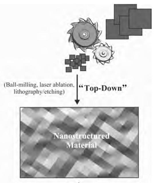
3 Top-Down methods Mechanical-energy methods Thermal fabrication methods High-energy and particle methods Lithographic methods Chemical methods Natural processes 3
4 Thermal methods Annealing Chill-block melt spinning Electrohydrodynamic atomization (EHDA) Electrospinning Liquid dynamic compaction (LDC) Gas atomization Evaporation Template extrusion Sublimation Thermolysis / Pyrolysis Combustion Polymer carbonization 4

5 Electrospinning High voltage is applied to a polymer melt solution to induce charging. Thin layers of filaments from a bulk polymer solution are able to generate fibers of nanoscale diameter. 5
6 Gas Atomization The idea is to transfer the kinetic energy from a supersonic jet of gas to a stream of liquid metal causing it to break up into droplets. 6
7 High-Energy methods Arc discharge Laser ablation Solar energy vaporization Plasma methods Ion milling Electron-beam evaporation Reactive ion etching (RIE) Pyrolysis Combustion High energy sonication 7

8 Arc -discharge methods Two carbon rods placed facing each other with about 1 mm gap, in an enclosure that is filled with either helium or argon gas. The arcvaporization of carbon creates nanotubes. The carbon arc discharge method is the most common and perhaps easiest way to produce CNTs. It is a technique that produces a complex mixture of components, and requires purification -to separate the CNTs from the soot and the residual catalytic metals present in the crude product. 8
9 Top-down Lithography Photolithography Immersion lithography Deep ultraviolet lithography (DUV) X-ray lithography (XRL) Electron-beam lithography Focused ion beam lithography (FIBL) Microcontact printing methods Nano imprint lithography (NIL) Nanosphere lithography (NSL) Scanning AFM nano-stencil Scanning probe nano-lithographies 9
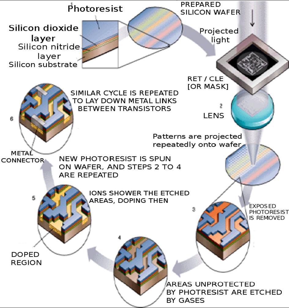
10 Lithographic Processing The word lithography comes from the Greek lithos, meaning stones, and graphia, meaning to write. It means quite literally writing on stones. In the case of semiconductor lithography (also called photolithography) our stones are silicon wafers and our patterns are written with a light sensitive polymer called a photoresist. To build the complex structures that make up a transistor and the many wires that connect the millions of transistors of a circuit, lithography and etch pattern transfer steps are repeated at least 10 times, but more typically are done 20 to 30 times to make one circuit. Each pattern being printed on the wafer is aligned to the previously formed patterns and slowly the conductors, insulators, and selectively doped regions are built up to form the final device. 10

11 Lithographic Processing Coat, protect, expose, etch, repeat Result: Multiple patterned layers of different materials. 11
12 Lithographic Processing The resist material is applied as a thin coating, typically by spin coating over the substrate (wafer) and then heated to remove the casting solvent (post-apply bake, pre-exposure bake, or pre-bake). The resist film is subsequently exposed in an image-wise fashion through a mask (in photoand X-ray lithography) or directly with finely focused electron beams. The exposed resist film is then developed typically by immersion in a developer solvent to generate three-dimensional relief images. The exposure may render the resist film more soluble in the developer, thereby producing a positive-tone image of the mask. Conversely, it may become less soluble upon exposure, resulting in generation of a negative-tone image. When the resist image is transferred into the substrate by etching and related processes, the resist film that remains after the development functions as a protective mask. The resist film must "resist" the etchant and protect the underlying substrate while the bared areas are being etched. The remaining resist film is finally stripped, leaving an image of the desired circuit in the substrate. The process is repeated many times to fabricate complex semiconductor devices. 12

13 Lithographic Processing 13
14 14
 is a direct write lithographic technique that uses an atomic force microscope (AFM) to build a pattern on the substrate material rather than etching it away.")
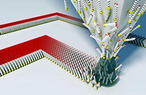
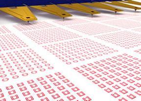
15 Dip-Pen Lithography Dip pen nanolithography can be used in a range of applications from semiconductor patterning and chip manufacturing to biomedical and pharmaceuticals development. Dip-Pen Nanolithography (DPN) is a direct write lithographic technique that uses an atomic force microscope (AFM) to build a pattern on the substrate material rather than etching it away. In the same way that an old fashioned dip pen picks up ink from an ink well and is then used to write on paper, molecules are picked up from a reservoir on the end of the AFM tip and deposited to the surface of the substrate via a solvent or water. 15
16 Dip-Pen Lithography 16

17 Lithographic Processing: Masking and Exposure 17
18 18
Fabrication Technology
 Fabrication Technology By B.G.Balagangadhar Department of Electronics and Communication Ghousia College of Engineering, Ramanagaram 1 OUTLINE Introduction Why Silicon The purity of Silicon Czochralski
Technology. Semiconductor Manufacturing. Hong Xiao INTRODUCTION TO SECOND EDITION SPIE PRESS
 INTRODUCTION TO Semiconductor Manufacturing Technology SECOND EDITION Hong Xiao TECHNISCHE INFORMATIONSBiBUOTHEK UNIVERSITATSBIBLIOTHEK HANNOVER SPIE PRESS Bellingham,Washington USA Contents Preface to
VLSI Technology. By: Ajay Kumar Gautam
 By: Ajay Kumar Gautam Introduction to VLSI Technology, Crystal Growth, Oxidation, Epitaxial Process, Diffusion Process, Ion Implantation, Lithography, Etching, Metallization, VLSI Process Integration,
Lecture 19 Microfabrication 4/1/03 Prof. Andy Neureuther
 EECS 40 Spring 2003 Lecture 19 Microfabrication 4/1/03 Prof. ndy Neureuther How are Integrated Circuits made? Silicon wafers Oxide formation by growth or deposition Other films Pattern transfer by lithography
Ajay Kumar Gautam [VLSI TECHNOLOGY] VLSI Technology for 3RD Year ECE/EEE Uttarakhand Technical University
![Ajay Kumar Gautam [VLSI TECHNOLOGY] VLSI Technology for 3RD Year ECE/EEE Uttarakhand Technical University](/thumbs/75/72824557.jpg "Ajay Kumar Gautam [VLSI TECHNOLOGY] VLSI Technology for 3RD Year ECE/EEE Uttarakhand Technical University") 2014 Ajay Kumar Gautam [VLSI TECHNOLOGY] VLSI Technology for 3RD Year ECE/EEE Uttarakhand Technical University Page1 Syllabus UNIT 1 Introduction to VLSI Technology: Classification of ICs, Scale of integration,
2014 Ajay Kumar Gautam [VLSI TECHNOLOGY] VLSI Technology for 3RD Year ECE/EEE Uttarakhand Technical University Page1 Syllabus UNIT 1 Introduction to VLSI Technology: Classification of ICs, Scale of integration,
PROCESSING OF INTEGRATED CIRCUITS
 PROCESSING OF INTEGRATED CIRCUITS Overview of IC Processing (Part I) Silicon Processing Lithography Layer Processes Use in IC Fabrication (Part II) Integrating the Fabrication Steps IC Packaging (Part
EE40 Lec 22. IC Fabrication Technology. Prof. Nathan Cheung 11/19/2009
 Suggested Reading EE40 Lec 22 IC Fabrication Technology Prof. Nathan Cheung 11/19/2009 300mm Fab Tour http://www-03.ibm.com/technology/manufacturing/technology_tour_300mm_foundry.html Overview of IC Technology
Metallization deposition and etching. Material mainly taken from Campbell, UCCS
 Metallization deposition and etching Material mainly taken from Campbell, UCCS Application Metallization is back-end processing Metals used are aluminum and copper Mainly involves deposition and etching,
Silicon Wafer Processing PAKAGING AND TEST
 Silicon Wafer Processing PAKAGING AND TEST Parametrical test using test structures regularly distributed in the wafer Wafer die test marking defective dies dies separation die fixing (not marked as defective)
Atomic Layer Deposition(ALD)
") Atomic Layer Deposition(ALD) AlO x for diffusion barriers OLED displays http://en.wikipedia.org/wiki/atomic_layer_deposition#/media/file:ald_schematics.jpg Lam s market-leading ALTUS systems combine CVD
Atomic Layer Deposition(ALD) AlO x for diffusion barriers OLED displays http://en.wikipedia.org/wiki/atomic_layer_deposition#/media/file:ald_schematics.jpg Lam s market-leading ALTUS systems combine CVD
Lecture 10: MultiUser MEMS Process (MUMPS)
") MEMS: Fabrication Lecture 10: MultiUser MEMS Process (MUMPS) Prasanna S. Gandhi Assistant Professor, Department of Mechanical Engineering, Indian Institute of Technology, Bombay, 1 Recap Various VLSI based
MEMS: Fabrication Lecture 10: MultiUser MEMS Process (MUMPS) Prasanna S. Gandhi Assistant Professor, Department of Mechanical Engineering, Indian Institute of Technology, Bombay, 1 Recap Various VLSI based
Photolithography I ( Part 2 )
") 1 Photolithography I ( Part 2 ) Chapter 13 : Semiconductor Manufacturing Technology by M. Quirk & J. Serda Bjørn-Ove Fimland, Department of Electronics and Telecommunication, Norwegian University of Science
1 Photolithography I ( Part 2 ) Chapter 13 : Semiconductor Manufacturing Technology by M. Quirk & J. Serda Bjørn-Ove Fimland, Department of Electronics and Telecommunication, Norwegian University of Science
Figure 2.3 (cont., p. 60) (e) Block diagram of Pentium 4 processor with 42 million transistors (2000). [Courtesy Intel Corporation.
 (e) Block diagram of Pentium 4 processor with 42 million transistors (2000). [Courtesy Intel Corporation.") Figure 2.1 (p. 58) Basic fabrication steps in the silicon planar process: (a) oxide formation, (b) selective oxide removal, (c) deposition of dopant atoms on wafer, (d) diffusion of dopant atoms into exposed
Figure 2.1 (p. 58) Basic fabrication steps in the silicon planar process: (a) oxide formation, (b) selective oxide removal, (c) deposition of dopant atoms on wafer, (d) diffusion of dopant atoms into exposed
Process Flow in Cross Sections
 Process Flow in Cross Sections Process (simplified) 0. Clean wafer in nasty acids (HF, HNO 3, H 2 SO 4,...) --> wear gloves! 1. Grow 500 nm of SiO 2 (by putting the wafer in a furnace with O 2 2. Coat
Lab #2 Wafer Cleaning (RCA cleaning)
") Lab #2 Wafer Cleaning (RCA cleaning) RCA Cleaning System Used: Wet Bench 1, Bay1, Nanofabrication Center Chemicals Used: H 2 O : NH 4 OH : H 2 O 2 (5 : 1 : 1) H 2 O : HF (10 : 1) H 2 O : HCl : H 2 O 2
Lab #2 Wafer Cleaning (RCA cleaning) RCA Cleaning System Used: Wet Bench 1, Bay1, Nanofabrication Center Chemicals Used: H 2 O : NH 4 OH : H 2 O 2 (5 : 1 : 1) H 2 O : HF (10 : 1) H 2 O : HCl : H 2 O 2
Visit
 Practical Applications for Nano- Electronics by Vimal Gopee E-mail: Vimal.gopee@npl.co.uk 10/10/12 Your Delegate Webinar Control Panel Open and close your panel Full screen view Raise hand for Q&A at the
Plasma Etching Rates & Gases Gas ratios affects etch rate & etch ratios to resist/substrate
 Plasma Etching Rates & Gases Gas ratios affects etch rate & etch ratios to resist/substrate Development of Sidewalls Passivating Films Sidewalls get inert species deposited on them with plasma etch Creates
From microelectronics down to nanotechnology.
 From microelectronics down to nanotechnology sami.franssila@tkk.fi Contents Lithography: scaling x- and y-dimensions MOS transistor physics Scaling oxide thickness (z-dimension) CNT transistors Conducting
Fabrication Techniques for Thin-Film Silicon Layer Transfer
 Fabrication Techniques for Thin-Film Silicon Layer Transfer S. L. Holl a, C. A. Colinge b, S. Song b, R. Varasala b, K. Hobart c, F. Kub c a Department of Mechanical Engineering, b Department of Electrical
Advanced developer-soluble gap-fill materials and applications
 Advanced developer-soluble gap-fill materials and applications Runhui Huang, Dan Sullivan, Anwei Qin, Shannon Brown Brewer Science, Inc., 2401 Brewer Dr., Rolla, MO, USA, 65401 ABSTRACT For the via-first
Vertically aligned Ni magnetic nanowires fabricated by diblock-copolymer-directed Al thin film anodization
 Vertically aligned Ni magnetic nanowires fabricated by diblock-copolymer-directed Al thin film anodization Researcher: Kunbae (Kevin) Noh, Graduate Student, MAE Dept. and CMRR Collaborators: Leon Chen,
KGC SCIENTIFIC Making of a Chip
 KGC SCIENTIFIC www.kgcscientific.com Making of a Chip FROM THE SAND TO THE PACKAGE, A DIAGRAM TO UNDERSTAND HOW CPU IS MADE? Sand CPU CHAIN ANALYSIS OF SEMICONDUCTOR Material for manufacturing process
Journal of Chemical and Pharmaceutical Research, 2017, 9(1): Research Article
: Research Article") Available online www.jocpr.com Journal of Chemical and Pharmaceutical Research, 2017, 9(1):163-167 Research Article ISSN : 0975-7384 CODEN(USA) : JCPRC5 Synthesis and Characterization of Carbon Nano Spheres
Available online www.jocpr.com Journal of Chemical and Pharmaceutical Research, 2017, 9(1):163-167 Research Article ISSN : 0975-7384 CODEN(USA) : JCPRC5 Synthesis and Characterization of Carbon Nano Spheres
Surface micromachining and Process flow part 1
 Surface micromachining and Process flow part 1 Identify the basic steps of a generic surface micromachining process Identify the critical requirements needed to create a MEMS using surface micromachining
Gaetano L Episcopo. Introduction to MEMS
 Gaetano L Episcopo Introduction to MEMS What are MEMS? Micro Electro Mechanichal Systems MEMS are integrated devices, or systems of devices, with microscopic parts, such as: Mechanical Parts Electrical
1. Introduction. What is implantation? Advantages
 Ion implantation Contents 1. Introduction 2. Ion range 3. implantation profiles 4. ion channeling 5. ion implantation-induced damage 6. annealing behavior of the damage 7. process consideration 8. comparison
Integration of Block-Copolymer with Nano- Imprint Lithography: Pushing the Boundaries of Emerging Nano-Patterning Technology
 Integration of Block-Copolymer with Nano- Imprint Lithography: Pushing the Boundaries of Emerging Nano-Patterning Technology April 2010 update SNL Geoff Brennecka (PI) Bruce Burckel Matt George Jack Skinner
Optimizing spray coater process parameters
 Optimizing spray coater process parameters Dr. Eleonora Storace, Florian Palitschka, Dr. Dietrich Tönnies SUSS MicroTec Lithography GmbH Germany Published in the SUSS report 01/2014 E-mail: info@suss.com
Process steps for Field Emitter devices built on Silicon wafers And 3D Photovoltaics on Silicon wafers
 Process steps for Field Emitter devices built on Silicon wafers And 3D Photovoltaics on Silicon wafers David W. Stollberg, Ph.D., P.E. Research Engineer and Adjunct Faculty GTRI_B-1 Field Emitters GTRI_B-2
Regents of the University of California
 Surface-Micromachining Process Flow Photoresist Sacrificial Oxide Structural Polysilcon Deposit sacrificial PSG: Target = 2 m 1 hr. 40 min. LPCVD @450 o C Densify the PSG Anneal @950 o C for 30 min. Lithography
CHAPTER 1 HOW SEMICONDUCTOR CHIPS ARE MADE
 CHAPTER 1 HOW SEMICONDUCTOR CHIPS ARE MADE Hwaiyu Geng Hewlett-Packard Company Palo Alto, California Lin Zhou Intel Corporation Hillsboro, Oregon 1.1 INTRODUCTION Over the past decades, an information
!"#$#%&#'(() ) **+,-./01)2-,-.3)456,1) /0! **)
 ) **+,-./01)2-,-.3)456,1) /0! **)") !"#$#%&#'(() ) **+,-./01)2-,-.3)456,1) /0!7.5853-09**) Etching Removal of unwanted or non-circuit copper from board Etch resists organic and metallic resists photoresist tin, gold, nickel, silver and alloys
!"#$#%&#'(() ) **+,-./01)2-,-.3)456,1) /0!7.5853-09**) Etching Removal of unwanted or non-circuit copper from board Etch resists organic and metallic resists photoresist tin, gold, nickel, silver and alloys
How To Write A Flowchart
 1 Learning Objectives To learn how you transfer a device concept into a process flow to fabricate the device in the EKL labs You learn the different components that makes up a flowchart; process blocks,
THE ASPECTS ABOUT RAPID PROTOTYPING SYSTEM
 THE ASPECTS ABOUT RAPID PROTOTYPING SYSTEM Adrian P. POP 1, Petru UNGUR 1, Gheorghe BEJINARU MIHOC 2 1 University of Oradea, e-mail: adippop@yahoo.com; petru_ungur@yahoo.com; 2 Transilvania University
EE C245 ME C218 Introduction to MEMS Design Fall 2011
 Lecture Outline EE C245 ME C218 Introduction to MEMS Design Fall 2011 Prof. Clark T.-C. Nguyen Dept. of Electrical Engineering & Computer Sciences University of California at Berkeley Berkeley, CA 94720
Leveraging the Precision of Electroforming over Alternative Processes When Developing Nano-scale Structures
 VOLUME 4 - ELECTROFORMING Leveraging the Precision of over Alternative Processes When Developing Nano-scale Structures Electrical and mechanical component and subsystem designers generally have five techniques
CMOS FABRICATION. n WELL PROCESS
 CMOS FABRICATION n WELL PROCESS Step 1: Si Substrate Start with p- type substrate p substrate Step 2: Oxidation Exposing to high-purity oxygen and hydrogen at approx. 1000 o C in oxidation furnace SiO
micro resist technology
 Characteristics Processing guidelines Negative Tone Photoresist Series ma-n 2400 ma-n 2400 is a negative tone photoresist series designed for the use in micro- and nanoelectronics. The resists are available
Carbon Nanotube Solutions for Packaging and Wireless Sensors
 Carbon Nanotube Solutions for Packaging and Wireless Sensors Jim Lamb*, Liyong Diao, Christopher Landorf Jordan Valley Innovation Center (JVIC) Springfield, Missouri, USA *jlamb@brewerscience.com APEC
Thermal Evaporation. Theory
 Thermal Evaporation Theory 1. Introduction Procedures for depositing films are a very important set of processes since all of the layers above the surface of the wafer must be deposited. We can classify
BASICS OF MANUFACTURING INTEGRATED CIRCUITS
 BASICS OF MANUFACTURING INTEGRATED CIRCUITS Opportunities for filtration exist for the manufacture of very small electronic components referred to as semiconductors. This broad category includes devices
Ion-Sensitive Field Effect Transistors for ph and Potassium ion concentration sensing, towards detection of Myocardial Ischemia.
 Ion-Sensitive Field Effect Transistors for ph and Potassium ion concentration sensing, towards detection of Myocardial Ischemia. Pratyush Rai a, Soyoun Jung b, Taeksoo Ji b, Vijay K Varadan b a Biomedical
Supporting Information
 Supporting Information Fast-Response, Sensitivitive and Low-Powered Chemosensors by Fusing Nanostructured Porous Thin Film and IDEs-Microheater Chip Zhengfei Dai,, Lei Xu,#,, Guotao Duan *,, Tie Li *,,
Processing guidelines. Negative Tone Photoresist Series ma-n 2400
 Characteristics Processing guidelines Negative Tone Photoresist Series ma-n 2400 ma-n 2400 is a negative tone photoresist series designed for the use in micro- and nanoelectronics. The resists are available
Delamination of Thin Films Using Laser Induced Stress Waves
 Center for Nanoscale Chemical-Electrical-Mechanical Manufacturing Systems Delamination of Thin Films Using Laser Induced Stress Waves Undergraduate Researcher Angelica Anne Vargas, Research Experience
Uncrosslinked SU-8 as a sacrificial material
 INSTITUTE OFPHYSICS PUBLISHING JOURNAL OF MICROMECHANICS AND MICROENGINEERING J. Micromech. Microeng. 15 (2005) N1 N5 doi:10.1088/0960-1317/15/1/n01 TECHNICAL NOTE Uncrosslinked as a sacrificial material
Photoresist Coat, Expose and Develop Laboratory Dr. Lynn Fuller
 ROCHESTER INSTITUTE OF TECHNOLOGY MICROELECTRONIC ENGINEERING Photoresist Coat, Expose and Develop Laboratory Dr. Lynn Fuller Webpage: http://www.rit.edu/lffeee 82 Lomb Memorial Drive Rochester, NY 14623-5604
COMPATIBILITY OF THE ALTERNATIVE SEED LAYER (ASL) PROCESS WITH MONO- Si AND POLY-Si SUBSTRATES PATTERNED BY LASER OR WET ETCHING
 PROCESS WITH MONO- Si AND POLY-Si SUBSTRATES PATTERNED BY LASER OR WET ETCHING") COMPATIBILITY OF THE ALTERNATIVE SEED LAYER (ASL) PROCESS WITH MONO- Si AND POLY-Si SUBSTRATES PATTERNED BY LASER OR WET ETCHING Lynne Michaelson 1, Anh Viet Nguyen 2, Krystal Munoz 1, Jonathan C. Wang
COMPATIBILITY OF THE ALTERNATIVE SEED LAYER (ASL) PROCESS WITH MONO- Si AND POLY-Si SUBSTRATES PATTERNED BY LASER OR WET ETCHING Lynne Michaelson 1, Anh Viet Nguyen 2, Krystal Munoz 1, Jonathan C. Wang
Alternative Methods of Yttria Deposition For Semiconductor Applications. Rajan Bamola Paul Robinson
 Alternative Methods of Yttria Deposition For Semiconductor Applications Rajan Bamola Paul Robinson Origin of Productivity Losses in Etch Process Aggressive corrosive/erosive plasma used for etch Corrosion/erosion
Micropatterning and casting PEDOT-PSS /DMSO layers
 Micropatterning and casting PEDOT-PSS /DMSO layers Benoît Charlot, Gilbert Sassine, Alexandra Garraud, Alain Giani, Philippe Combette IES Institut d Electronique du Sud CNRS Université Montpellier II Place&E.&Bataillon,&34095&Montpellier&7&France&
Nanofabrication Prof. Stephen Y. Chou NanoStructure Laboratory
 Nanofabrication Prof. Stephen Y. Chou Department of Electrical Engineering Princeton University 1 Acknowledgment Dr. Paul Fischer Dr. Yun Wang Dr. Jay Guo Dr. Peter Klauss Dr. Jim Wang Dr. Longtin He Dr.
Photonic Drying Pulsed Light as a low Temperature Sintering Process
 Photonic Drying Pulsed Light as a low Temperature Sintering Process Lou Panico Xenon Corporation W E S T E R N M I C H I G A N U N I V E R S I T Y PRESENTATION OVERVIEW What is Printed Electronics Materials
FY06 ACCOMPLISHMENTS. Nanoelectronics Manufacture, Inspection, and Repair using Thermal Dip Pen Nanolithography
 FY06 ACCOMPLISHMENTS Nanoelectronics Manufacture, Inspection, and Repair using Thermal Dip Pen Nanolithography William P. King Georiga Institute of Technology FY06 was the second year of this grant, and
LANDOLT-BÖRNSTEIN. Zahlenwerte und Funktionen aus Naturwissenschaften und Technik. Neue Serie. Gesamtherausgabe: K.-H. Hellwege O.
 LANDOLT-BÖRNSTEIN Zahlenwerte und Funktionen aus Naturwissenschaften und Technik Neue Serie Gesamtherausgabe: K.-H. Hellwege O. Madelung Gruppe III: Kristall- und Festkörperphysik Band 17 Halbleiter Herausgeber:
Semiconductor Manufacturing Technology. IC Fabrication Process Overview
 Semiconductor Manufacturing Technology Michael Quirk & Julian Serda October 00 by Prentice Hall Chapter 9 IC Fabrication Process Overview /4 Objectives After studying the material in this chapter, you
R Sensor resistance (Ω) ρ Specific resistivity of bulk Silicon (Ω cm) d Diameter of measuring point (cm)
 ρ Specific resistivity of bulk Silicon (Ω cm) d Diameter of measuring point (cm)") 4 Silicon Temperature Sensors 4.1 Introduction The KTY temperature sensor developed by Infineon Technologies is based on the principle of the Spreading Resistance. The expression Spreading Resistance derives
4 Silicon Temperature Sensors 4.1 Introduction The KTY temperature sensor developed by Infineon Technologies is based on the principle of the Spreading Resistance. The expression Spreading Resistance derives
Mater. Res. Soc. Symp. Proc. Vol Materials Research Society
 Mater. Res. Soc. Symp. Proc. Vol. 940 2006 Materials Research Society 0940-P13-12 A Novel Fabrication Technique for Developing Metal Nanodroplet Arrays Christopher Edgar, Chad Johns, and M. Saif Islam
MCC. PMGI Resists NANO PMGI RESISTS OFFER RANGE OF PRODUCTS
 MCC PMGI RESISTS OFFER Sub.25µm lift-off processing Film thicknesses from 5µm Choice of resin blends for optimal undercut control High thermal stability Superior adhesion to Si, NiFe, GaAs, InP
LOW TEMPERATURE PHOTONIC SINTERING FOR PRINTED ELECTRONICS. Dr. Saad Ahmed XENON Corporation November 19, 2015
 LOW TEMPERATURE PHOTONIC SINTERING FOR PRINTED ELECTRONICS Dr. Saad Ahmed XENON Corporation November 19, 2015 Topics Introduction to Pulsed Light Photonic sintering for Printed Electronics R&D Tools for
A Deep Silicon RIE Primer Bosch Etching of Deep Structures in Silicon
 A Deep Silicon RIE Primer Bosch Etching of Deep Structures in Silicon April 2009 A Deep Silicon RIE Primer 1.0) Etching: Silicon does not naturally etch anisotropically in fluorine based chemistries. Si
Oligomer-Coated Carbon Nanotube Chemiresistive Sensors for Selective Detection of Nitroaromatic Explosives
 Supporting information for Oligomer-Coated Carbon Nanotube Chemiresistive Sensors for Selective Detection of Nitroaromatic Explosives Yaqiong Zhang, Miao Xu, Benjamin R. Bunes, Na Wu, Dustin E. Gross,,
Lecture Day 2 Deposition
 Deposition Lecture Day 2 Deposition PVD - Physical Vapor Deposition E-beam Evaporation Thermal Evaporation (wire feed vs boat) Sputtering CVD - Chemical Vapor Deposition PECVD LPCVD MVD ALD MBE Plating
Oxide Growth. 1. Introduction
 Oxide Growth 1. Introduction Development of high-quality silicon dioxide (SiO2) has helped to establish the dominance of silicon in the production of commercial integrated circuits. Among all the various
CMOS Manufacturing process. Circuit designer. Design rule set. Process engineer. Set of optical masks. Fabrication process.
 CMOS Manufacturing process Circuit design Set of optical masks Fabrication process Circuit designer Design rule set Process engineer All material: Chap. 2 of J. Rabaey, A. Chandrakasan, B. Nikolic, Digital
Lecture 6. Through-Wafer Interconnect. Agenda: Through-wafer Interconnect Polymer MEMS. Through-Wafer Interconnect -1. Through-Wafer Interconnect -2
 Agenda: EEL6935 Advanced MEMS (Spring 2005) Instructor: Dr. Huikai Xie Lecture 6 Through-wafer Interconnect EEL6935 Advanced MEMS 2005 H. Xie 1/21/2005 1 Motivations: Wafer-level packaging CMOS 3D Integration
Isolation of elements
 1 In an IC, devices on the same substrate must be isolated from one another so that there is no current conduction between them. Isolation uses either the junction or dielectric technique or a combination
Via Fill in Small Trenches using Hot Aluminum Process. By Alice Wong
 Via Fill in Small Trenches using Hot Aluminum Process By Alice Wong Goals for Project Good Via Fill in Small contact holes using hot aluminum process Be able to get good images of the contact holes using
3.155J / 6.152J Micro/Nano Processing Technology TAKE-HOME QUIZ FALL TERM 2005
 3.155J / 6.152J Micro/Nano Processing Technology TAKE-HOME QUIZ FALL TERM 2005 1) This is an open book, take-home quiz. You are not to consult with other class members or anyone else. You may discuss the
VLSI Systems and Computer Architecture Lab
 ΚΥΚΛΩΜΑΤΑ VLSI Πανεπιστήμιο Ιωαννίνων CMOS Technology Τμήμα Μηχανικών Η/Υ και Πληροφορικής 1 From the book: An Introduction ti to VLSI Process By: W. Maly ΚΥΚΛΩΜΑΤΑ VLSI Διάρθρωση 1. N well CMOS 2. Active
CNT Reinforced Nanocomposite Fiber Fabrication for Undergraduate Students
 CNT Reinforced Nanocomposite Fiber Fabrication for Undergraduate Students 1 Asmatulu, R., 1 Khan, W., and 2 Yildirim, M.B. Abatract 1 Department of Mechanical Engineering, Wichita State University 1845
ME 189 Microsystems Design and Manufacture. Chapter 9. Micromanufacturing
 ME 189 Microsystems Design and Manufacture Chapter 9 Micromanufacturing This chapter will offer an overview of the application of the various fabrication techniques described in Chapter 8 in the manufacturing
Towards scalable fabrication of high efficiency polymer solar cells
 Towards scalable fabrication of high efficiency polymer solar cells Hui Joon Park 2*, Myung-Gyu Kang 1**, Se Hyun Ahn 3, Moon Kyu Kang 1, and L. Jay Guo 1,2,3 1 Department of Electrical Engineering and
Isolation Technology. Dr. Lynn Fuller
 ROCHESTER INSTITUTE OF TECHNOLOGY MICROELECTRONIC ENGINEERING Isolation Technology Dr. Lynn Fuller Motorola Professor 82 Lomb Memorial Drive Rochester, NY 14623-5604 Tel (585) 475-2035 Fax (585) 475-5041
NONTRADITIONAL MACHINING AND THERMAL CUTTING PROCESSES
 NONTRADITIONAL MACHINING AND THERMAL CUTTING PROCESSES Mechanical Energy Processes Electrochemical Machining Processes Thermal Energy Processes Chemical Machining Application Considerations Nontraditional
Comparison of Atmospheric Plasma and Corona Treatments in Promoting Seal Strength
 Comparison of Atmospheric Plasma and Corona Treatments in Promoting Seal Strength Presented by Rory Wolf Business Unit Manager ITW Pillar Technologies Discussion Agenda o Study Objective o Extrusion Coating
In-Situ Monitoring of Pattern Filling in Nano-Imprint Lithography Using Surface Plasmon Resonance
 Copyright 2011 American Scientific Publishers All rights reserved Printed in the United States of America Journal of Nanoscience and Nanotechnology Vol. 11, 1 6, 2011 In-Situ Monitoring of Pattern Filling
Fabrication of aligned metallic structures based on block copolymer lithography
 88 Fabrication of aligned metallic structures based on block copolymer lithography Yusuke Takahashi Department ofmicroelectronic Engineering, Rochester Institute of Technology, 82 Lomb Memorial Dr., Rochester,
St.JOHNS COLLEGE OF ENGINEERING AND TECHNOLOGY,
 PRESENTED BY S.SRIKANTH REDDY Y.MARUTHI III B.tech III.B.tech Sri.prince087@gmail.com St.JOHNS COLLEGE OF ENGINEERING AND TECHNOLOGY, YERRAKOTA, YEMIGANUR, KURNOOL (Dist), ANDHRA PRADESH. ABSTRACT VLSI
5.8 Diaphragm Uniaxial Optical Accelerometer
 5.8 Diaphragm Uniaxial Optical Accelerometer Optical accelerometers are based on the BESOI (Bond and Etch back Silicon On Insulator) wafers, supplied by Shin-Etsu with (100) orientation, 4 diameter and
Available online at ScienceDirect. Procedia Materials Science 10 (2015 )
") Available online at www.sciencedirect.com ScienceDirect Procedia Materials Science 10 (2015 ) 254 262 2nd International Conference on Nanomaterials and Technologies (CNT 2014) Enhancing the Performance
Available online at www.sciencedirect.com ScienceDirect Procedia Materials Science 10 (2015 ) 254 262 2nd International Conference on Nanomaterials and Technologies (CNT 2014) Enhancing the Performance
UTILIZATION OF ATMOSPHERIC PLASMA SURFACE PREPARATION TO IMPROVE COPPER PLATING PROCESSES.
 SESSION 14 MATERIALS AND PROCESSES FOR ADVANCED PACKAGING UTILIZATION OF ATMOSPHERIC PLASMA SURFACE PREPARATION TO IMPROVE COPPER PLATING PROCESSES. Eric Schulte 1, Gilbert Lecarpentier 2 SETNA Corporation
Today s agenda (19-JAN-2010)
") Today s agenda (19-JAN-2010) 1) Overview of Integrated Circuit technology 2) Managing Deadlines 3) A look @ Spring Schedule 4) Suggested milestones 5) Project concept presentations Action items from last
Today s agenda (19-JAN-2010) 1) Overview of Integrated Circuit technology 2) Managing Deadlines 3) A look @ Spring Schedule 4) Suggested milestones 5) Project concept presentations Action items from last
A Quick Overview of Micromachining for MEMS Designers
 A Quick Overview of Micromachining for MEMS Designers A designer has control over two sets of variables: materials and the shapes of parts. M. F. Ashby Manufacturing determines which materials can be processed
Lecture 12. Physical Vapor Deposition: Evaporation and Sputtering Reading: Chapter 12. ECE Dr. Alan Doolittle
 Lecture 12 Physical Vapor Deposition: Evaporation and Sputtering Reading: Chapter 12 Evaporation and Sputtering (Metalization) Evaporation For all devices, there is a need to go from semiconductor to metal.
FIB mask repair technology for EUV mask 1. INTRODUCTION
 FIB mask repair technology for EUV mask Tsuyoshi Amano*, Yasushi Nishiyama*, iroyuki Shigemura*, Tsuneo Terasawa*, Osamu Suga*, Kensuke Shiina**, Fumio Aramaki**, Anto Yasaka** Tsukasa Abe***, iroshi Mohri***
Nontraditional Machining Processes
 Nontraditional Machining Processes The NTM processes can be divided into four basic categories: I. Chemical (Chemical reaction), II. Electrochemical (Electrolytic dissolution), III. Mechanical (Multipoint
Galvanic Porous Silicon for High Velocity Nanoenergetics
 Supporting Information Galvanic Porous Silicon for High Velocity Nanoenergetics Collin R. Becker 1,2, Steven Apperson 3, Christopher J. Morris 2, Shubhra Gangopadhyay 3, Luke J. Currano 2, Wayne A. Churaman
Micro-Electro-Mechanical Systems (MEMS) Fabrication. Special Process Modules for MEMS. Principle of Sensing and Actuation
 Fabrication. Special Process Modules for MEMS. Principle of Sensing and Actuation") Micro-Electro-Mechanical Systems (MEMS) Fabrication Fabrication Considerations Stress-Strain, Thin-film Stress, Stiction Special Process Modules for MEMS Bonding, Cavity Sealing, Deep RIE, Spatial forming
Micro-Electro-Mechanical Systems (MEMS) Fabrication Fabrication Considerations Stress-Strain, Thin-film Stress, Stiction Special Process Modules for MEMS Bonding, Cavity Sealing, Deep RIE, Spatial forming
Lecture 030 Integrated Circuit Technology - I (5/8/03) Page 030-1
 Page 030-1") Lecture 030 Integrated Circuit Technology - I (5/8/03) Page 030-1 LECTURE 030 INTEGRATED CIRCUIT TECHNOLOGY - I (References [7,8]) Objective The objective of this presentation is: 1.) Illustrate integrated
Lecture 030 Integrated Circuit Technology - I (5/8/03) Page 030-1 LECTURE 030 INTEGRATED CIRCUIT TECHNOLOGY - I (References [7,8]) Objective The objective of this presentation is: 1.) Illustrate integrated
MCC. NANO PMMA and Copolymer
 MCC PRODUCT ATTRIBUTES NANO and Submicron linewidth control (polymethyl methacrylate) is a versatile polymeric material that is well suited Sub 0.1µm imaging for many imaging and non-imaging microelectronic
NANO SCRATCH TESTING OF THIN FILM ON GLASS SUBSTRATE
 NANO SCRATCH TESTING OF THIN FILM ON GLASS SUBSTRATE Prepared by Jesse Angle 6 Morgan, Ste156, Irvine CA 92618 P: 949.461.9292 F: 949.461.9232 nanovea.com Today's standard for tomorrow's materials. 2010
Multiphoton lithography based 3D micro/nano printing Dr Qin Hu
 Multiphoton lithography based 3D micro/nano printing Dr Qin Hu EPSRC Centre for Innovative Manufacturing in Additive Manufacturing University of Nottingham Multiphoton lithography Also known as direct
SOIMUMPs Design Handbook
 SOIMUMPs Design Handbook a MUMPs process C. J. Han, Allen Cowen, Greg Hames and Busbee Hardy MEMScAP Revision 3.0 Copyright 2002 by MEMScAP. All rights reserved. Permission to use and copy for internal,
Final Year Project Proposal 1
 Final Year Project Proposal 1 Mechanical testing for high temperature polymers Mr Eric Phua Jian Rong (JRPhua@ntu.edu.sg) In offshore subsea drilling, different types of microelectronics devices and sensors
Filling and Planarizing Deep Trenches with Polymeric Material for Through-Silicon Via Technology
 Filling and Planarizing Deep Trenches with Polymeric Material for Through-Silicon Via Technology R.K. Trichur, M. Fowler, J.W. McCutcheon, and M. Daily Brewer Science, Inc. 2401 Brewer Drive Rolla, MO
National Nanotechnology Infrastructure Network Vol.3 # 1. A Periodic Newsletter of NNIN News and Announcements NNIN. New Equipment and Processes
 National Nanotechnology Infrastructure Network Vol.3 # 1 A Periodic Newsletter of NNIN News and Announcements Feb. 2007 NNIN The National Nanotechnology Infrastructure Network consists of 13 nanotechnology
Cost of Integrated Circuits
 Cost of IC Design 1 Cost of Integrated Circuits NRE (Non-Recurrent Engineering) costs fixed design time and effort, mask generation independent of sales volume / number of products one-time cost factor
High-Resolution, Electrohydrodynamic Inkjet Printing of Stretchable, Metal Oxide Semiconductor Transistors with High Performances
 Electronic Supplementary Material (ESI) for Nanoscale. This journal is The Royal Society of Chemistry 2016 ` Electronic Supplementary Information High-Resolution, Electrohydrodynamic Inkjet Printing of
A Novel Method for Low-Resistivity Metal-Interconnection by Using Metallic Functional Liquids and Catalytically Generated Hydrogen Atoms.
 A Novel Method for Low-Resistivity Metal-Interconnection by Using Metallic Functional Liquids and Catalytically Generated Hydrogen Atoms. Journal: 2011 MRS Fall Meeting Manuscript ID: Draft Manuscript
Linear Plasma Sources for Surface Modification and Deposition for Large Area Coating
 Linear Plasma Sources for Surface Modification and Deposition for Large Area Coating Dr Tony Williams Gencoa Ltd, UK Victor Bellido-Gonzalez, Dr Dermot Monaghan, Dr Joseph Brindley, Robert Brown SVC 2016,