Nano-imprinting Lithography Technology І
|
|
|
- Adam McGee
- 6 years ago
- Views:
Transcription
1 Nano-imprinting Lithography Technology І
2 Agenda Limitation of photolithograph - Remind of photolithography technology - What is diffraction - Diffraction limit Concept of nano-imprinting lithography Basic process of nano-imprinting lithography technology
3 Remind of photolithography technology Photoresist process for lithography Clean substrate Development Apply Adhesion Promoter(HMDS) PR Spin Coating Post Baking Soft Baking Etching Limitation of photolithography UV Exposure Remove PR
4 Photolithography process and limitation UV Exposure Mask Ideal case of photolithography UV Exposure Real case of photolithography (ultra small pattern size) 회절로인해같은조건의촬영시위와같은상이한결과를초래 Diffraction effect (Image blur 현상발생 )

5 What is diffraction? Diffraction is the process by which light waves traveling through a small hole, slit or around a boundary will spread out Basic assumption : Light is wave
6 What is diffraction? Diffraction causes the loss of resolving power Image blur 현상은각종수차에의해영향을받지만공기중의 particle 에의한 diffraction 으로인해같은조건의촬영시위와같은상이한결과를초래한다

7 Diffraction limit Example Diffraction of circular aperture is a Bessel function of the first kind

8 Diffraction limit The radius of the Airy disk D θ
9 Nano-imprinting Lithography Technology II


10 Imprinting 현존하는가장오래된금속활자본직지심체요절 < 금속활자본 > < 목판본 > < 금속활자본표지 > 정식명칭 : 백운화상초록불조직지심체요절 1377년 ( 고려우왕 3) 7월청주흥덕사간행 세계에서가장오래된금속활자본 1372년쓰여진책을 77년금속, 78년목판으로간행 금속활자본은현재프랑스국립도서관에소장 2001년유네스코세계기록유산등재 자료출처 :
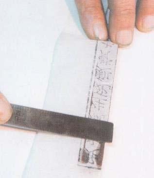
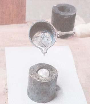
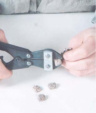
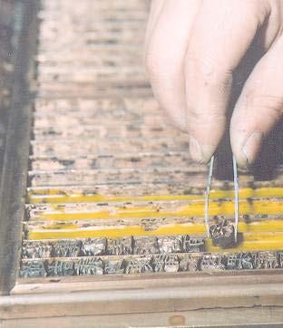
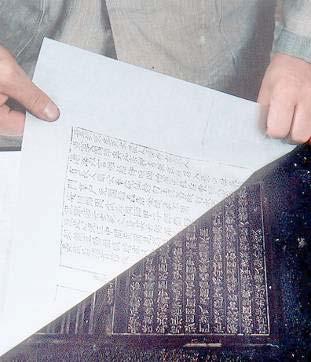
11 Imprinting 직지심체요절금속활자제작및인쇄과정 < 글자본선정 > < 자본붙이기 > < 어미자만들기 > < 주형틀만들기 > < 쇳물붓기 > < 활자떼어내기 > < 조판 > < 인쇄 > 자료출처 :

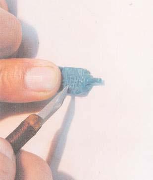
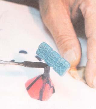
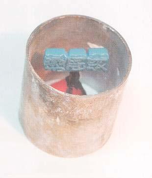
12 Nano-imprinting process 1. Mold fabricaion step - Using E-beam lithography, FIB, etc. 1. Mold fabrication Mold 2. Press mold Mold < Mold > 2. Imprinting step - Nano mold with nano-scale pattern is pressed into a resist 3. Remove mold Resist Substrate Mold Resist Substrate < Resist pattern >
13 Nano-imprinting 기술의종류


 - RIE is used to remove the residual resist")

14 Basic process of nano-imprinting lithography technology Procedure of nanoimprinting lithography : 2 basic step 1. Imprint step - Nano mold with nano-scale pattern is pressed into a resist 2. Pattern transfer step - Pattern transfer to substrate by RIE (Reactive Ion Etching) - RIE is used to remove the residual resist in the compressed area 1. Pressing mold 2. Remove mold mold resist resist substrate mold resist resist substrate < Mold > 3. Pattern transfer (RIE) resist substrate < Resist pattern > 자료출처 : Proc. SPIE 4349, (2001), p. 82


15 Thermal nano-imprinting lithography technology Procedures Heating of Substrate and Mold to above Tg 1. Press mold with heat Application of Molding Pressure Cooling of Substrate and Mold to below Tg 2. Remove mold Mold Resist Substrate Mold < Mold > Demolding Resist Substrate 자료출처 : < Imprinted resist >


16 UV nano-imprinting lithography technology UV nano-imprinting Material: UV-curable photopolymer Processing condition: room temp. & low pressure No fluidity problem Procedures <Lattice pattern> <Pyramid pattern> Substrate Photopolymer UV-transparent mold Photopolymer dispensation on substrate Covering the mold Aligning UV-light Releasing the mold Pressure 자료출처 : JJAP, vol. 44, No. 7B, pp. 5600, 2005


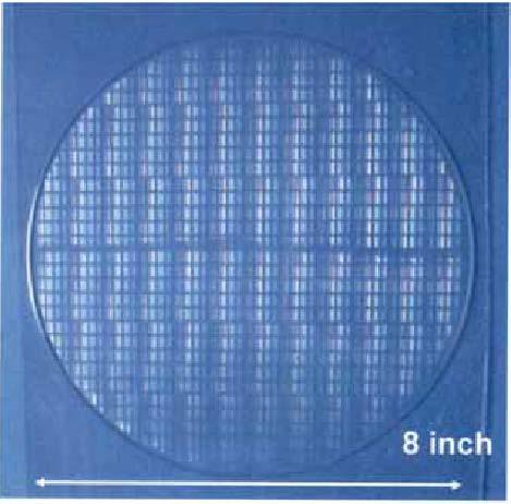
17 Continuous UV nano-imprinting lithography technology Design and construction of continuous UV nano imprinting system Continuous UV nano-imprinting system For flexible substrate For rigid substrate Fabrication results 1. Can replicate nano patterns of large area with high precision 2. Can replace conventional lithography process
18 Imprinting system

19 EVG 社 EVG 620 bond aligner Precise wafer/substrate alignment for wafer bonding applications High-resolution bottom side splitfield microscope 1 µm alignment accuracy Easy to use Windows based operation

20 .. SUSS 社 NPS 300 (Nano patterning stepper) 250 nm overlay accuracy Unmatched sub-20 nm embossing capability Submicron Stamp-to-Wafer alignment with state-of-the-art pattern recognition system

21 Molecular Imprint 社 Imprio 250 Resolution: Sub-50 nm Alignment: < 10 nm Flexibility: 200 mm and 300mm substrates with automated loading Field size: 26 x 32 mm active print area.
 Good pattern uniformity 6 inch direct")
22 Nano & Device 社 Nanosis 610 No align option Near zero residual layer UV curing & hot embossing (universal) Good pattern uniformity 6 inch direct imprinting
23 Issues of nanoimprinting Fabrication of nano master / mold Thickness of residual layer Large area patterning Demolding Imprinting material Mass productivity and system itself
24 Nano Imprinting Lithography Technology III
25 Agenda Thickness of residual layer Mass productivity and system itself - Large area patterning - Mass productivity
26 Thickness of residual layer
 Pressure UV- curing This")
27 What is residual layer? UV-transparent mold Imprinting material (photopolymer) Pressure UV- curing This is the residual layer! After the residual layer etching
28 Importance of thickness of residual layer Purpose of the nano imprinting lithography Use the pattern itself - AR Surface - Optical nano grating - Wave guider - Nano structure for optoelectronic devices Use the pattern as a barrier for after process - Replace the photolithography process
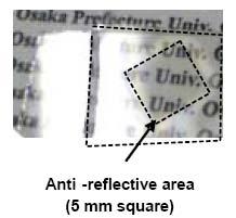
29 AR coating on mold AR coating (Anti reflection coating) UV Reflection of UV Mold without AR coating PHotopolymer Optical substrate has about 4% reflection in general AR coating on mold surface is very important

30 Importance of thickness of residual layer Nano structure for optoelectronic devices (MLA on VCSEL) n 1 R n 1 R Emitting area n 1 R VCSEL array Bonding pad VCSEL Micro-Lens Fiber We must control the residual layer for designed focal length
31 Importance of thickness of residual layer Use the pattern as a barrier for after process (critical reason) UV-transparent mold UV photopolymer Preparation Mold lamination and Appling pressure UV curing Demolding Remove the residual layer Etch the substrate Remove the photopolymer 이때 pattern 의크기에비해너무두꺼운 residual layer 가남아있다면 이를제거할때 pattern 은모두손실되고만다

32 Zero residual layer process Conventional imprint Zero residual imprint
33 Application of nano-imprinting technology I


34 Super hydrophobic surface 연꽃잎 자료출처 : Manhui Sun, Langmuir, Vol.21, pp.8978, 2005 L. Feng, Advanced Material,Vol.14, pp.1857, 2002 Alexander Otten, Langmuir, Vol.20, pp.2405, 2004


35 Super hydrophobic surface 연꽃잎의모사 응용분야 매미날개의모사 < 자동차 > 자료출처 : Manhui Sun et at al.,langmuir, vol.21, pp.8978, 2005 Woo Lee et at al., Langmuir, Vol.20, pp.7665, < 유리창 >


36 Anti-reflective surface 나방의눈 자료출처 :


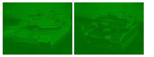
37 Anti-reflective surface 나방눈의모사패턴 무반사면의응용 자료출처 : MNE 06 Micro- and Nano- Engineering Kenji Sogo, Journal of Photopolymer Science Technology, Vol.19, pp.647, 2006


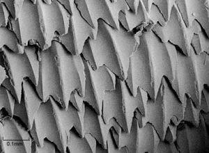
38 Drag reduction of surface 상어의피부 자료출처 : D. W. Bechert, Naturwissenschaften, Vol. 87, pp.157, 2004


39 Drag reduction of surface 상어피부 상어피부형상의응용 - 수영복 10% 감소효과 <Drag reduction of surface> 자료출처 : D. W. Bechert, Naturwissenschaften, Vol. 87, pp.157, 2004 <Speedo Fastskin II>
40 Application of nano-imprinting technology II

41 Bio chip fabrication using nano-imprinting Imprinting of bio chip 자료출처 : macrogen.co.kr

42 Bio chip fabrication using nano-imprinting

43 Lab-on-a-chip fabrication using nano-imprinting LOC with microfluidic channels 자료출처 :
Photolithography I ( Part 2 )
") 1 Photolithography I ( Part 2 ) Chapter 13 : Semiconductor Manufacturing Technology by M. Quirk & J. Serda Bjørn-Ove Fimland, Department of Electronics and Telecommunication, Norwegian University of Science
1 Photolithography I ( Part 2 ) Chapter 13 : Semiconductor Manufacturing Technology by M. Quirk & J. Serda Bjørn-Ove Fimland, Department of Electronics and Telecommunication, Norwegian University of Science
Processing guidelines
 Processing guidelines mr-uvcur21 series UV-curable Polymer for UV-based Nanoimprint Lithography Characteristics mr-uvcur21 is a liquid UV-curable polymer system with low viscosity and high curing rate
Photoresist Coat, Expose and Develop Laboratory Dr. Lynn Fuller
 ROCHESTER INSTITUTE OF TECHNOLOGY MICROELECTRONIC ENGINEERING Photoresist Coat, Expose and Develop Laboratory Dr. Lynn Fuller Webpage: http://www.rit.edu/lffeee 82 Lomb Memorial Drive Rochester, NY 14623-5604
Micro and nano structuring of carbon based materials for micro injection moulding and hot embossing
 Micro and nano structuring of carbon based materials for micro injection moulding and hot embossing Victor Usov, Graham Cross, Neal O Hara, Declan Scanlan, Sander Paulen, Chris de Ruijter, Daniel Vlasveld,
Technical Data Sheet Technisches Datenblatt
 AZ ECI 3000 Photoresist Universal i-line/crossover Photoresist Series GENERAL INFORMATION AZ ECI 3000 photoresist series are a family of fast positive resists with high resolution capabilities (0.4 µm
Multiphoton lithography based 3D micro/nano printing Dr Qin Hu
 Multiphoton lithography based 3D micro/nano printing Dr Qin Hu EPSRC Centre for Innovative Manufacturing in Additive Manufacturing University of Nottingham Multiphoton lithography Also known as direct
Leveraging the Precision of Electroforming over Alternative Processes When Developing Nano-scale Structures
 VOLUME 4 - ELECTROFORMING Leveraging the Precision of over Alternative Processes When Developing Nano-scale Structures Electrical and mechanical component and subsystem designers generally have five techniques
Lab #2 Wafer Cleaning (RCA cleaning)
") Lab #2 Wafer Cleaning (RCA cleaning) RCA Cleaning System Used: Wet Bench 1, Bay1, Nanofabrication Center Chemicals Used: H 2 O : NH 4 OH : H 2 O 2 (5 : 1 : 1) H 2 O : HF (10 : 1) H 2 O : HCl : H 2 O 2
Lab #2 Wafer Cleaning (RCA cleaning) RCA Cleaning System Used: Wet Bench 1, Bay1, Nanofabrication Center Chemicals Used: H 2 O : NH 4 OH : H 2 O 2 (5 : 1 : 1) H 2 O : HF (10 : 1) H 2 O : HCl : H 2 O 2
micro resist technology
 Characteristics Processing guidelines Negative Tone Photoresist Series ma-n 2400 ma-n 2400 is a negative tone photoresist series designed for the use in micro- and nanoelectronics. The resists are available
TSV Processing and Wafer Stacking. Kathy Cook and Maggie Zoberbier, 3D Business Development
 TSV Processing and Wafer Stacking Kathy Cook and Maggie Zoberbier, 3D Business Development Outline Why 3D Integration? TSV Process Variations Lithography Process Results Stacking Technology Wafer Bonding
Nanofabrication Prof. Stephen Y. Chou NanoStructure Laboratory
 Nanofabrication Prof. Stephen Y. Chou Department of Electrical Engineering Princeton University 1 Acknowledgment Dr. Paul Fischer Dr. Yun Wang Dr. Jay Guo Dr. Peter Klauss Dr. Jim Wang Dr. Longtin He Dr.
In-Situ Monitoring of Pattern Filling in Nano-Imprint Lithography Using Surface Plasmon Resonance
 Copyright 2011 American Scientific Publishers All rights reserved Printed in the United States of America Journal of Nanoscience and Nanotechnology Vol. 11, 1 6, 2011 In-Situ Monitoring of Pattern Filling
Step and Flash Imprint Lithography for sub-100nm Patterning
 Step and Flash Imprint Lithography for sub-100nm Patterning Matthew Colburn, Annette Grot, Marie Amistoso, Byung Jin Choi, Todd Bailey, John Ekerdt, S.V. Sreenivasan, James Hollenhorst, C. Grant Willson
Integration of Block-Copolymer with Nano- Imprint Lithography: Pushing the Boundaries of Emerging Nano-Patterning Technology
 Integration of Block-Copolymer with Nano- Imprint Lithography: Pushing the Boundaries of Emerging Nano-Patterning Technology April 2010 update SNL Geoff Brennecka (PI) Bruce Burckel Matt George Jack Skinner
Processing guidelines. Negative Tone Photoresist Series ma-n 2400
 Characteristics Processing guidelines Negative Tone Photoresist Series ma-n 2400 ma-n 2400 is a negative tone photoresist series designed for the use in micro- and nanoelectronics. The resists are available
Vacuum casting, a new answer for manufacturing biomicrosystems
 1 Vacuum casting, a new answer for manufacturing biomicrosystems M Denoual 1 *, P Mognol 2, and B Lepioufle 1 1 Biomis-SATIE ENS-Cachan antenne de Bretagne, Bruz, France 2 IRCCyN Nantes, France The manuscript
High-throughput three-dimensional (3D) lithographic microfabrication in biomedical applications
 lithographic microfabrication in biomedical applications") High-throughput three-dimensional (3D) lithographic microfabrication in biomedical applications The MIT Faculty has made this article openly available. Please share how this access benefits you. Your story
High-throughput three-dimensional (3D) lithographic microfabrication in biomedical applications The MIT Faculty has made this article openly available. Please share how this access benefits you. Your story
EXPLORING VACUUM CASTING TECHNIQUES FOR MICRON AND SUBMICRON FEATURES. Campus Ker Lann, av Robert Schumann Bruz, France
 EXPLORING VACUUM CASTING TECHNIQUES FOR MICRON AND SUBMICRON FEATURES M. Denoual *, P. Mognol **, B. Lepioufle * * Biomis-SATIE ENS-Cachan antenne de Bretagne, Campus Ker Lann, av Robert Schumann 35170
NTT-AT Optical Adhesives Lineup. Adhesives / Resins and Sealants for Optical Component Assembly
 NTT-AT Optical Adhesives Lineup Adhesives / Resins and Sealants for Optical Component Assembly The adhesive technology used in optical communications is one of the key technologies we offer. Ask us anything
TSV Interposer Process Flow with IME 300mm Facilities
 TSV Interposer Process Flow with IME 300mm Facilities Property of Institute of Microelectronics (IME)-Singapore August 17, 2012 Outline 1. TSV interposer (TSI) cross sectional schematic TSI with BEOL,
EV Group 300mm Wafer Bonding Technology July 16, 2008
 EV Group 300mm Wafer Bonding Technology July 16, 2008 EV Group in a Nutshell st Our philosophy Our mission in serving next generation application in semiconductor technology Equipment supplier for the
ULTRA-SMALL VIA-TECHNOLOGY OF THINFILM POLYMERS USING ADVANCED SCANNING LASER ABLATION
 ULTRA-SMALL VIA-TECHNOLOGY OF THINFILM POLYMERS USING ADVANCED SCANNING LASER ABLATION Michael Töpper Fraunhofer Research Institution for Reliability and Microintegration IZM Germany Martin Wilke, Klaus-Dieter
Precision Electroforming in High-Strength NiColoy
 Taking the Stress out of Electroforming www.nicoform.com Precision Electroforming in High-Strength NiColoy Copyright 2007 NiCoForm, Inc. (Rochester, NY) Electroforming What is it? What is it good for?
Nanoimprint Lithography - Next Generation Nanopatterning Methods for Nanophotonics Fabrication
 14 Nanoimprint Lithography - Next Generation Nanopatterning Methods for Nanophotonics Fabrication Jukka Viheriälä, Tapio Niemi, Juha Kontio and Markus Pessa Optoelectronics Research Centre, Tampere University
Report 1. B. Starting Wafer Specs Number: 10 Total, 6 Device and 4 Test wafers
 Aaron Pederson EE 432 Lab Dr. Meng Lu netid: abp250 Lab instructor: Yunfei Zhao Report 1 A. Overview The goal of this lab is to go through the semiconductor fabrication process from start to finish. This
Electronically switchable diffractive optical elements
 Electronically switchable diffractive optical elements GARRY LESTER, ADRIAN STRUDWICK AND * STEPHEN COULSTON L-lectronics Ltd, 48 Wilton Way, Exeter, EX 3UR * QuantX (Oxford), North Leigh Business Park,
Positive Photoresists
 Positive Photoresists Gesellschaft für chemische Materialien spezieller Photoresistsysteme mbh Positive Photoresists map 1200 series Thick resists map 1275, map 1275 HV Unique features of the positive
Micro Injection Molding of Micro Fluidic Platform
 Micro Injection Molding of Micro Fluidic Platform S. C. Chen, J. A. Chang, Y. J. Chang and S. W. Chau Department of Mechanical Engineering, Chung Yuan University, Taiwan, ROC Abstract In this study, micro
D Eggenstein-Leopoldshafen, Germany 2 University of Karlsruhe (TH), Institute for Microstructure Technology (IMT),
, Institute for Microstructure Technology (IMT),") Sub-µ structured Lotus Surfaces Manufacturing M. Worgull 1, M. Heckele 1, T. Mappes 2, B. Matthis 1, G. Tosello 3, T. Metz 4, J. Gavillet 5, P. Koltay 4, H. N. Hansen 3 1 Forschungszentrum Karlsruhe (FZK),
Sub-µ structured Lotus Surfaces Manufacturing M. Worgull 1, M. Heckele 1, T. Mappes 2, B. Matthis 1, G. Tosello 3, T. Metz 4, J. Gavillet 5, P. Koltay 4, H. N. Hansen 3 1 Forschungszentrum Karlsruhe (FZK),
EE40 Lec 22. IC Fabrication Technology. Prof. Nathan Cheung 11/19/2009
 Suggested Reading EE40 Lec 22 IC Fabrication Technology Prof. Nathan Cheung 11/19/2009 300mm Fab Tour http://www-03.ibm.com/technology/manufacturing/technology_tour_300mm_foundry.html Overview of IC Technology
Procese de depunere in sistemul Plasma Enhanced Chemical Vapor Deposition (PECVD)
") Procese de depunere in sistemul Plasma Enhanced Chemical Vapor Deposition (PECVD) Ciprian Iliescu Conţinutul acestui material nu reprezintă in mod obligatoriu poziţia oficială a Uniunii Europene sau a
Procese de depunere in sistemul Plasma Enhanced Chemical Vapor Deposition (PECVD) Ciprian Iliescu Conţinutul acestui material nu reprezintă in mod obligatoriu poziţia oficială a Uniunii Europene sau a
SUSS SOLUTIONS FOR LARGE FORMAT PATTERNING UV Scanning Lithography and Excimer Laser Ablation
 SUSS SOLUTIONS FOR LARGE FORMAT PATTERNING UV Scanning Lithography and Excimer Laser Ablation Kevin Yang, Habib Hichri, Ralph Zoberbier SÜSS MicroTec Photonic Systems Inc. June 18, 2015 MARKET DRIVER Mobile
Via Fill in Small Trenches using Hot Aluminum Process. By Alice Wong
 Via Fill in Small Trenches using Hot Aluminum Process By Alice Wong Goals for Project Good Via Fill in Small contact holes using hot aluminum process Be able to get good images of the contact holes using
125nXT Series. EMD PeRFoRmaNce MaTeRIaLs. technical datasheet. Photopolymer Negative Tone Photoresists APPLICATION TYPICAL PROCESS THICKNESS GRADES
 EMD PeRFoRmaNce MaTeRIaLs technical datasheet AZ 125nXT Series Photopolymer Negative Tone Photoresists APPLICATION Thick photopolymer photoresists featuring aspect ratios and photospeed not possible with
Micro-Electro-Mechanical Systems (MEMS) Fabrication. Special Process Modules for MEMS. Principle of Sensing and Actuation
 Fabrication. Special Process Modules for MEMS. Principle of Sensing and Actuation") Micro-Electro-Mechanical Systems (MEMS) Fabrication Fabrication Considerations Stress-Strain, Thin-film Stress, Stiction Special Process Modules for MEMS Bonding, Cavity Sealing, Deep RIE, Spatial forming
Micro-Electro-Mechanical Systems (MEMS) Fabrication Fabrication Considerations Stress-Strain, Thin-film Stress, Stiction Special Process Modules for MEMS Bonding, Cavity Sealing, Deep RIE, Spatial forming
Large-area patterning by roller-based nanoimprint lithography
 JOANNEUM RESEARCH Forschungsgesellschaft Institute MATERIALS, Weiz, Austria Large-area patterning by roller-based nanoimprint lithography Ursula Palfinger, Dieter Nees, Stephan Ruttloff, Markus Leitgeb,
5.8 Diaphragm Uniaxial Optical Accelerometer
 5.8 Diaphragm Uniaxial Optical Accelerometer Optical accelerometers are based on the BESOI (Bond and Etch back Silicon On Insulator) wafers, supplied by Shin-Etsu with (100) orientation, 4 diameter and
FABRICATION FOR MICRO PATTERNS OF NICKEL MATRIX DIAMOND COMPOSITES USING THE COMPOSITE ELECTROFORMING AND UV- LITHOGRAPHY
 16 TH INTERNATIONAL CONFERENCE ON COMPOSITE MATERIALS FABRICATION FOR MICRO PATTERNS OF NICKEL MATRIX DIAMOND COMPOSITES USING THE COMPOSITE ELECTROFORMING AND UV- LITHOGRAPHY Tsung-Han Yu, Shenq-Yih Luo,
UV5 POSITIVE DUV PHOTORESIST For Microlithography Applications
 UV5 POSITIVE DUV PHOTORESIST For Microlithography Applications DESCRIPTION UV5 positive DUV photoresist has been optimized to provide vertical profile imaging of isolated and semidense features for device
Assembly of Mechanically Compliant Interfaces between Optical Fibers and Nanophotonic Chips
 Assembly of Mechanically Compliant Interfaces between Optical Fibers and Nanophotonic Chips T. Barwicz, Y. Taira, H. Numata, N. Boyer, S. Harel, S. Kamlapurkar, S. Takenobu, S. Laflamme, S. Engelmann,
Soft-lithography for Preparing Patterned Liquid Crystal Orientations
 2007 KIDS Soft-lithography for Preparing Patterned Liquid Crystal Orientations Hak-Rin Kim **a, Jong-Wook Jung **a, Min-Soo Shin **a, Myung-Eun Kim a, You-Jin Lee **a, and Jae-Hoon Kim *b Abstract We demonstrate
Novel Materials and Activities for Next Generation Package. Hitachi Chemical., Co.Ltd. Packaging Solution Center Hiroaki Miyajima
 Novel Materials and Activities for Next Generation Package Hitachi Chemical., Co.Ltd. Packaging Solution Center Hiroaki Miyajima 1. Activities of Packaging Solution Center 2. Novel Materials for Next Gen.
Process Flow in Cross Sections
 Process Flow in Cross Sections Process (simplified) 0. Clean wafer in nasty acids (HF, HNO 3, H 2 SO 4,...) --> wear gloves! 1. Grow 500 nm of SiO 2 (by putting the wafer in a furnace with O 2 2. Coat
How To Write A Flowchart
 1 Learning Objectives To learn how you transfer a device concept into a process flow to fabricate the device in the EKL labs You learn the different components that makes up a flowchart; process blocks,
THIN FILM THICKNESS MEASUREMENT FOR EVALUATION OF RESIDUAL LAYER OF NANO-IMPRINT LITHOGRAPHY USING NEAR-FIELD OPTICS
 9 th INTERNATIONAL SYMPOSIUM ON MEASUREMENT AND QUALITY CONTROL (9 th ISMQC) November 21 24, 27, IIT Madras THIN FILM THICKNESS MEASUREMENT FOR EVALUATION OF RESIDUAL LAYER OF NANO-IMPRINT LITHOGRAPHY
FABRICATION AND RELIABILITY OF ULTRA-FINE RDL STRUCTURES IN ADVANCED PACKAGING BY EXCIMER LASER ABLATION
 FABRICATION AND RELIABILITY OF ULTRA-FINE RDL STRUCTURES IN ADVANCED PACKAGING BY EXCIMER LASER ABLATION NCCAVS Joint Users Group Technical Symposium San Jose, June 7 th, 2017 Markus Arendt, SÜSS MicroTec
Superionic Solid State Stamping (S4)
") Superionic Solid State Stamping (S4) Lead Faculty Researcher: Placid Ferreira Department: Materials Science & Engineering Hsu et al, Nano Letters, 2007 1. Description: This dry, single step, electrochemical
Superionic Solid State Stamping (S4) Lead Faculty Researcher: Placid Ferreira Department: Materials Science & Engineering Hsu et al, Nano Letters, 2007 1. Description: This dry, single step, electrochemical
Mater. Res. Soc. Symp. Proc. Vol Materials Research Society
 Mater. Res. Soc. Symp. Proc. Vol. 940 2006 Materials Research Society 0940-P13-12 A Novel Fabrication Technique for Developing Metal Nanodroplet Arrays Christopher Edgar, Chad Johns, and M. Saif Islam
Process steps for Field Emitter devices built on Silicon wafers And 3D Photovoltaics on Silicon wafers
 Process steps for Field Emitter devices built on Silicon wafers And 3D Photovoltaics on Silicon wafers David W. Stollberg, Ph.D., P.E. Research Engineer and Adjunct Faculty GTRI_B-1 Field Emitters GTRI_B-2
Lecture 6. Through-Wafer Interconnect. Agenda: Through-wafer Interconnect Polymer MEMS. Through-Wafer Interconnect -1. Through-Wafer Interconnect -2
 Agenda: EEL6935 Advanced MEMS (Spring 2005) Instructor: Dr. Huikai Xie Lecture 6 Through-wafer Interconnect EEL6935 Advanced MEMS 2005 H. Xie 1/21/2005 1 Motivations: Wafer-level packaging CMOS 3D Integration
Precise Ion and Electron Beam Processing for Nano-Structuring
 Precise Ion and Electron Beam Processing for Nano-Structuring Regina Korntner, Hans Loeschner and Elmar Platzgummer Vienna, Austria 1 Outline Short Introduction to IMS Technology Introduction History of
SEPARATING PLASMA AND BLOOD CELLS BY DIELECTROPHORESIS IN MICROFLUIDIC CHIPS
 Fourth International Symposium on Physics of Fluids (ISPF4) International Journal of Modern Physics: Conference Series Vol. 19 (2012) 185 189 World Scientific Publishing Company DOI: 10.1142/S2010194512008732
Amorphous Oxide Transistor Electrokinetic Reflective Display on Flexible Glass
 Amorphous Oxide Transistor Electrokinetic Reflective Display on Flexible Glass Devin A. Mourey, Randy L. Hoffman, Sean M. Garner *, Arliena Holm, Brad Benson, Gregg Combs, James E. Abbott, Xinghua Li*,
LOW TEMPERATURE PHOTONIC SINTERING FOR PRINTED ELECTRONICS. Dr. Saad Ahmed XENON Corporation November 19, 2015
 LOW TEMPERATURE PHOTONIC SINTERING FOR PRINTED ELECTRONICS Dr. Saad Ahmed XENON Corporation November 19, 2015 Topics Introduction to Pulsed Light Photonic sintering for Printed Electronics R&D Tools for
KGC SCIENTIFIC Making of a Chip
 KGC SCIENTIFIC www.kgcscientific.com Making of a Chip FROM THE SAND TO THE PACKAGE, A DIAGRAM TO UNDERSTAND HOW CPU IS MADE? Sand CPU CHAIN ANALYSIS OF SEMICONDUCTOR Material for manufacturing process
Lecture 19 Microfabrication 4/1/03 Prof. Andy Neureuther
 EECS 40 Spring 2003 Lecture 19 Microfabrication 4/1/03 Prof. ndy Neureuther How are Integrated Circuits made? Silicon wafers Oxide formation by growth or deposition Other films Pattern transfer by lithography
Packaging Commercial CMOS Chips for Lab on a Chip Integration
 Supporting Information for Packaging Commercial CMOS Chips for Lab on a Chip Integration by Timir Datta-Chaudhuri, Pamela Abshire, and Elisabeth Smela Biocompatibility Although the supplier s instructions
Specimen Preparation Technique for a Microstructure Analysis Using the Focused Ion Beam Process
 Specimen Preparation Technique for a Microstructure Analysis Using the Focused Ion Beam Process by Kozue Yabusaki * and Hirokazu Sasaki * In recent years the FIB technique has been widely used for specimen
Metallization deposition and etching. Material mainly taken from Campbell, UCCS
 Metallization deposition and etching Material mainly taken from Campbell, UCCS Application Metallization is back-end processing Metals used are aluminum and copper Mainly involves deposition and etching,
MICROFABRICATION OF OPTICALLY ACTIVE InO X MICROSTRUCTURES BY ULTRASHORT LASER PULSES
 Journal of Optoelectronics and Advanced Materials Vol. 4, No. 3, September 2002, p. 809-812 MICROFABRICATION OF OPTICALLY ACTIVE InO X MICROSTRUCTURES BY ULTRASHORT LASER PULSES Foundation for Research
Fabrication Technology
 Fabrication Technology By B.G.Balagangadhar Department of Electronics and Communication Ghousia College of Engineering, Ramanagaram 1 OUTLINE Introduction Why Silicon The purity of Silicon Czochralski
Materials Characterization for Stress Management
 Materials Characterization for Stress Management Ehrenfried Zschech, Fraunhofer IZFP Dresden, Germany Workshop on Stress Management for 3D ICs using TSVs San Francisco/CA, July 13, 2010 Outline Stress
Lecture 10: MultiUser MEMS Process (MUMPS)
") MEMS: Fabrication Lecture 10: MultiUser MEMS Process (MUMPS) Prasanna S. Gandhi Assistant Professor, Department of Mechanical Engineering, Indian Institute of Technology, Bombay, 1 Recap Various VLSI based
MEMS: Fabrication Lecture 10: MultiUser MEMS Process (MUMPS) Prasanna S. Gandhi Assistant Professor, Department of Mechanical Engineering, Indian Institute of Technology, Bombay, 1 Recap Various VLSI based
Gaetano L Episcopo. Introduction to MEMS
 Gaetano L Episcopo Introduction to MEMS What are MEMS? Micro Electro Mechanichal Systems MEMS are integrated devices, or systems of devices, with microscopic parts, such as: Mechanical Parts Electrical
Novel Spin on Planarization Technology by Photo Curing SOC (P-SOC)
") Journal of Photopolymer Science and Technology Volume 3, Number 3 (17) 373-378 C 17SPST Technical Paper Novel Spin on Planarization Technology by Photo Curing (P-) Takafumi Endo*, Rikimaru Sakamoto, Keisuke
Journal of Photopolymer Science and Technology Volume 3, Number 3 (17) 373-378 C 17SPST Technical Paper Novel Spin on Planarization Technology by Photo Curing (P-) Takafumi Endo*, Rikimaru Sakamoto, Keisuke
Mold Fabrication for 3D Dual Damascene Imprinting
 Nanoscale Res Lett (2010) 5:545 549 DOI 10.1007/s11671-010-9540-2 SPECIAL ISSUE ARTICLE Mold Fabrication for 3D Dual Damascene Imprinting S. M. Saydur Rahman Bo Cui Received: 11 September 2009 / Accepted:
Lecture 5. SOI Micromachining. SOI MUMPs. SOI Micromachining. Silicon-on-Insulator Microstructures. Agenda:
 EEL6935 Advanced MEMS (Spring 2005) Instructor: Dr. Huikai Xie SOI Micromachining Agenda: SOI Micromachining SOI MUMPs Multi-level structures Lecture 5 Silicon-on-Insulator Microstructures Single-crystal
The Effect of Hydrophobic Patterning on Micromolding of Aqueous-Derived Silk Structures
 The Effect of Hydrophobic Patterning on Micromolding of Aqueous-Derived Silk Structures Konstantinos Tsioris 1, Robert D White 1, David L Kaplan 2, and Peter Y Wong 1 1 Mechanical Engineering, Tufts University,
Supporting informations
 Supporting informations Microfluidic with integrated microfilter of conical-shaped holes for high efficiency and high purity capture of circulating tumor cells Yadong Tang 1+, Jian Shi 2+, Sisi Li 1, Li
Hybrid BARC approaches for FEOL and BEOL integration
 Hybrid BARC approaches for FEOL and BEOL integration Willie Perez a, Stephen Turner a, Nick Brakensiek a, Lynne Mills b, Larry Wilson b, Paul Popa b a Brewer Science, Inc., 241 Brewer Dr., Rolla, MO 6541
Fabrication of a Crossbar Structure at 50 nm Half-pitch by UV-based Nanoimprint Lithography
 Fabrication of a 34 34 Crossbar Structure at 50 nm Half-pitch by UV-based Nanoimprint Lithography NANO LETTERS xxxx Vol. 0, No. 0 A-E G. Y. Jung, S. Ganapathiappan, Douglas A. A. Ohlberg, Deirdre L. Olynick,
Supporting Information
 Supporting Information Fast-Response, Sensitivitive and Low-Powered Chemosensors by Fusing Nanostructured Porous Thin Film and IDEs-Microheater Chip Zhengfei Dai,, Lei Xu,#,, Guotao Duan *,, Tie Li *,,
Proceedings Post Fabrication Processing of Foundry MEMS Structures Exhibiting Large, Out-of-Plane Deflections
 Proceedings Post Fabrication Processing of Foundry MEMS Structures Exhibiting Large, Out-of-Plane Deflections LaVern Starman 1, *, John Walton 1, Harris Hall 1 and Robert Lake 2 1 Sensors Directorate,
Semiconductor Manufacturing Technology. IC Fabrication Process Overview
 Semiconductor Manufacturing Technology Michael Quirk & Julian Serda October 00 by Prentice Hall Chapter 9 IC Fabrication Process Overview /4 Objectives After studying the material in this chapter, you
R&D ACTIVITIES AT ASSCP-BHEL,GURGAON IN SOLAR PV. DST-EPSRC Workshop on Solar Energy Research
 R&D ACTIVITIES AT -BHEL,GURGAON IN SOLAR PV at the DST-EPSRC Workshop on Solar Energy Research (22 nd 23 rd April, 2009) by Dr.R.K. Bhogra, Addl. General Manager & Head Email: cpdrkb@bhel.co.in Dr.A.K.
Ultra High Barrier Coatings by PECVD
 Society of Vacuum Coaters 2014 Technical Conference Presentation Ultra High Barrier Coatings by PECVD John Madocks & Phong Ngo, General Plasma Inc., 546 E. 25 th Street, Tucson, Arizona, USA Abstract Silicon
Status of the DESY NanoLab Project
 Status of the DESY NanoLab Project Ralf Röhlsberger DESY Wissenschaftlicher Ausschuss DESY 7 June 2011 Mission of the DESY NanoLab To accomodate the growing need for structural probes on the nanoscale,
Vertically aligned Ni magnetic nanowires fabricated by diblock-copolymer-directed Al thin film anodization
 Vertically aligned Ni magnetic nanowires fabricated by diblock-copolymer-directed Al thin film anodization Researcher: Kunbae (Kevin) Noh, Graduate Student, MAE Dept. and CMRR Collaborators: Leon Chen,
Metallic Antireflection Structures Made from Silver Ink by a Liquid Transfer Imprint Lithography Technique
 Journal of Photopolymer Science and Technology Volume 30, Number 5 (2017) 539-544 C 2017SPST Metallic Antireflection Structures Made from Silver Ink by a Liquid Transfer Imprint Lithography Technique Ichiro
Delamination of Thin Films Using Laser Induced Stress Waves
 Center for Nanoscale Chemical-Electrical-Mechanical Manufacturing Systems Delamination of Thin Films Using Laser Induced Stress Waves Undergraduate Researcher Angelica Anne Vargas, Research Experience
Advanced developer-soluble gap-fill materials and applications
 Advanced developer-soluble gap-fill materials and applications Runhui Huang, Dan Sullivan, Anwei Qin, Shannon Brown Brewer Science, Inc., 2401 Brewer Dr., Rolla, MO, USA, 65401 ABSTRACT For the via-first
Optimizing spray coater process parameters
 Optimizing spray coater process parameters Dr. Eleonora Storace, Florian Palitschka, Dr. Dietrich Tönnies SUSS MicroTec Lithography GmbH Germany Published in the SUSS report 01/2014 E-mail: info@suss.com
Measurement of thickness of native silicon dioxide with a scanning electron microscope
 Measurement of thickness of native silicon dioxide with a scanning electron microscope V. P. Gavrilenko* a, Yu. A. Novikov b, A. V. Rakov b, P. A. Todua a a Center for Surface and Vacuum Research, 40 Novatorov
EE C245 ME C218 Introduction to MEMS Design Fall 2011
 Lecture Outline EE C245 ME C218 Introduction to MEMS Design Fall 2011 Prof. Clark T.-C. Nguyen Dept. of Electrical Engineering & Computer Sciences University of California at Berkeley Berkeley, CA 94720
3.155J / 6.152J Micro/Nano Processing Technology TAKE-HOME QUIZ FALL TERM 2005
 3.155J / 6.152J Micro/Nano Processing Technology TAKE-HOME QUIZ FALL TERM 2005 1) This is an open book, take-home quiz. You are not to consult with other class members or anyone else. You may discuss the
Electron microscopy II
 Electron microscopy II Nanomaterials characterization I RNDr. Věra Vodičková, PhD. Interaction ction: electrons solid matter Signal types SE.secondary e - AE Auger s e - BSE back scattered e - X-ray photons,
Deep Lithography for Microfabrication
 Deep Lithography for Microfabrication Part 2: UV Deep Lithography (UVDL) Luiz O. S. Ferreira Mechanical Engineering Faculty Campinas State University UNICAMP Campinas SP - BRAZIL lotavio@fem.unicamp.br
MCC. NANO PMMA and Copolymer
 MCC PRODUCT ATTRIBUTES NANO and Submicron linewidth control (polymethyl methacrylate) is a versatile polymeric material that is well suited Sub 0.1µm imaging for many imaging and non-imaging microelectronic
Ajay Kumar Gautam [VLSI TECHNOLOGY] VLSI Technology for 3RD Year ECE/EEE Uttarakhand Technical University
![Ajay Kumar Gautam [VLSI TECHNOLOGY] VLSI Technology for 3RD Year ECE/EEE Uttarakhand Technical University](/thumbs/75/72824557.jpg "Ajay Kumar Gautam [VLSI TECHNOLOGY] VLSI Technology for 3RD Year ECE/EEE Uttarakhand Technical University") 2014 Ajay Kumar Gautam [VLSI TECHNOLOGY] VLSI Technology for 3RD Year ECE/EEE Uttarakhand Technical University Page1 Syllabus UNIT 1 Introduction to VLSI Technology: Classification of ICs, Scale of integration,
2014 Ajay Kumar Gautam [VLSI TECHNOLOGY] VLSI Technology for 3RD Year ECE/EEE Uttarakhand Technical University Page1 Syllabus UNIT 1 Introduction to VLSI Technology: Classification of ICs, Scale of integration,
MCC. PMGI Resists NANO PMGI RESISTS OFFER RANGE OF PRODUCTS
 MCC PMGI RESISTS OFFER Sub.25µm lift-off processing Film thicknesses from 5µm Choice of resin blends for optimal undercut control High thermal stability Superior adhesion to Si, NiFe, GaAs, InP
Avatrel Stress Buffer Coatings: Low Stress Passivation and Redistribution Applications
 Avatrel Stress Buffer Coatings: Low Stress Passivation and Redistribution Applications Ed Elce, Chris Apanius, Jeff Krotine, Jim Sperk, Andrew Bell, Rob Shick* Sue Bidstrup-Allen, Paul Kohl Takashi Hirano,
IMPLEMENTATION OF A FULLY MOLDED FAN-OUT PACKAGING TECHNOLOGY
 IMPLEMENTATION OF A FULLY MOLDED FAN-OUT PACKAGING TECHNOLOGY B. Rogers, C. Scanlan, and T. Olson Deca Technologies, Inc. Tempe, AZ USA boyd.rogers@decatechnologies.com ABSTRACT Fan-Out Wafer-Level Packaging
Bulk MEMS Fabrication Blog 2017 Dr. Lynn Fuller, Casey Gonta, Patsy Cadareanu
 ROCHESTER INSTITUTE OF TECHNOLOGY MICROELECTRONIC ENGINEERING Bulk MEMS Fabrication Blog 2017 Dr. Lynn Fuller, Casey Gonta, Patsy Cadareanu Webpage: http://people.rit.edu/lffeee 82 Lomb Memorial Drive
Sub-5 nm Structures Process Development and Fabrication Over Large Areas
 A S Jugessur,, 2017, 1:1 SciFed Nanotech Research Letters Research Article Open Access Sub-5 nm Structures Process Development and Fabrication Over Large Areas * A S Jugessur * University of Iowa Microfabrication
Semicon Europa Wafer Chucks for Lithography. Berliner Glas KGaA Herbert Kubatz GmbH & Co. Sven Götze
 Semicon Europa 2011. Wafer Chucks for Lithography. Berliner Glas KGaA Herbert Kubatz GmbH & Co. Sven Götze 1 Export driven, medium-sized, innovative. Solutions in Optics High Tech in Glass Legal form:
Nanocoating close to the market
 Nanocoating close to the market Moritz Graf zu Eulenburg Introduction Market overview Overview of most important coating aspects Description of different coating systems Description of different drying
Plasma for Underfill Process in Flip Chip Packaging
 Plasma for Underfill Process in Flip Chip Packaging Jack Zhao and James D. Getty Nordson MARCH 2470-A Bates Avenue Concord, California 94520-1294 USA Published by Nordson MARCH www.nordsonmarch.com 2015
Microcontact Printing Procedures for Adhesive and Conductive Epoxies
 Microcontact Printing Procedures for Adhesive and Conductive Epoxies This objective was accomplished through a formal record of the procedures to deliver a stamped product which met the benchmark mechanical,
BOROFLOAT & Glass Wafers: A Union of Inspiration & Quality
 Home Tech SCHOTT North America, Inc. 553 Shepherdsville Road Louisville, KY 4228 USA Phone: +1 (52) 657-4417 Fax: +1 (52) 966-4976 Email: borofloat@us.schott.com www.us.schott.com/borofloat/wafer BOROFLOAT
High-Speed Roll-to-Roll Nanoimprint Lithography on Flexible Plastic Substrates**
 COMMUNICATION DOI: 10.1002/adma.200702650 High-Speed Roll-to-Roll Nanoimprint Lithography on Flexible Plastic Substrates** By Se Hyun Ahn and L. Jay Guo* The ability of micro- to nanometer-scale patterning