Faceted inversion domain boundary in GaN films doped with Mg
|
|
|
- Maude Mitchell
- 6 years ago
- Views:
Transcription
1 Faceted inversion domain boundary in GaN films doped with Mg L. T. Romano* and J.E. Northrup Xerox Palo Alto Research Center, 3333 Coyote Hill Road, Palo Alto, CA A. J. Ptak and T.H. Myers Department of Physics, West Virginia University, Morgantown, West Virginia Key words: GaN films, Mg doping, inversion, faceting, total energy calculations Homoepitaxial GaN films doped with Mg were grown by rf-plasma molecular beam epitaxy on Ga-polarity (0001) MOCVD templates. Convergent beam electron diffraction analysis establishes that the film polarity changes from [0001] to [0001] when the Mg flux during growth is approximately one monolayer per second. Secondary ion mass spectrometry indicates a doping concentration of ~10 20 cm -3 in the film where the inversion occurs and shows a reduced Mg incorporation efficiency after further growth. Transmission electron microscopy shows that the inversion domain boundary is faceted predominantly along the {0001} and {h,h,-2h,l} planes, with l/h approximately equal to 3. Using first-principles total energy calculations we show that the {h,h,-2h,l} segments of the boundary are stabilized by the incorporation of Mg in threefold coordinated lattice sites. * romano@parc.xerox.com 1
2 Because magnesium is the most common dopant used to achieve p-type conductivity in the Ga(Al)N alloys employed in optoelectronic devices [1], its incorporation during growth has been the subject of a number of recent studies. [1-6] These studies have shown that the incorporation of high levels of Mg is often accompanied by the formation of extended defects. In single crystals of bulk-grown GaN:Mg, the presence of enclosed pyramidal defects and an ordered array of Mg-rich basal plane faults has been reported. [3]. Pyramidal defects have also been observed following the annealing of GaN:Mg layers at 1400 o C [4]. These enclosed pyramidal defects have been identified as inversion domains with boundaries lying in (0001) and {1123} planes [2]. Studies of GaN films grown by molecular beam epitaxy [5] have shown that exposure of the (0001) surface to ~ 1 ML of Mg can cause an inversion of polarity from Ga-face to N-face, and transmission electron microscopy images [5] have revealed the presence of inverted regions in Mg-doped layers of films grown by metal organic chemical vapor deposition (MOCVD). In this paper transmission electron microscopy (TEM) is used to study the microstructure of Mg-doped GaN films grown by rf-plasma molecular beam epitaxy (MBE). The substrates used for this study were undoped GaN films grown by MOCVD on c-plane sapphire. Films were also grown directly on c-plane sapphire for comparison. Convergent beam electron diffraction (CBED) was used to determine the polarity of the films. The MOCVD substrates were found to have [0001] polarity (Ga-face) whereas the films grown directly on sapphire had [0001] polarity (N-face). The Mg flux was controlled during growth by varying the effusion cell temperature (T Mg ) in a stepwise fashion over a temperature range from 250 o C to 400 o C. GaN spacer layers that were ~ 0.1 microns thick and nominally undoped were grown between the doped layers. Secondary ion mass spectrometry (SIMS) was used to determine the Mg concentration [Mg]. Cross sectional TEM analysis (XTEM) was performed on samples that were polished along the {1100} and {1120} directions and then argon ion thinned to electron transparency using a liquid nitrogen cold stage and low voltage to minimize damage. Figure 1 shows a SIMS profile for a Mg step-doped film grown at 710 o C on a MOCVD substrate. This and other SIMS measurements [7] suggest that a Mgaccumulation layer may be forming during the growth since the doping profile is not as 2
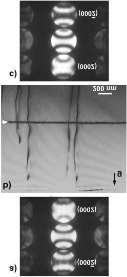
3 abrupt as the growth profile, and the undoped spacer layers are not clearly observed. For T Mg = 250 o C, the Mg concentration [Mg] in the film was below detectable levels. The average [Mg] was ~ 2 x cm -3 at T Mg = 300 o C and increased to ~ 8 x cm -3 at T Mg = 350 o C. Then, after T Mg was increased to 400 o C, there was a sharp decrease in the [Mg] to values below cm -3. At this point in the growth, T Mg was cycled through the same temperature range of o C. Even though hydrogen was present during this second cycle, which tends to increase the Mg incorporation rate [7], the SIMS data shows that the concentration of Mg incorporated was significantly reduced for the same corresponding values of T Mg used in the first cycle. The lower [Mg] obtained in the second cycle is, however, consistent with doping profiles measured for N-face polarity MBE films grown directly on sapphire [7], thus suggesting the possibility that the polarity of the film is inverted by the Mg exposure. A bright field TEM image of this film is shown in Fig. 2 along with convergent beam diffraction patterns. A low magnification image (Fig. 2b) indicates the existence of a structural interface where the Mg concentration was observed to drop in the SIMS profile. We note that structural interfaces were not observed between the MOCVD and MBE-grown layers or at any of the other doping changes (not shown). Threading dislocations from the MOCVD substrate are found to extend through this interface with some bending in the vicinity of the interface. To check for an inversion of the film polarity, convergent beam electron diffraction (CBED) was performed along the <1100> axis in regions of the film above and below the interface. The <1100> direction is conveniently chosen since it has inversion symmetry and the diffraction disks are well separated [8]. The sample thickness was kept constant during the measurement since the contrast within the diffractions disks is thickness dependent [9]. The results are shown in Figs. 2a and 2c. The contrast within the zero order disk is the same in both patterns which corresponds to a sample thickness, t ~ 125nm, by comparing to computer simulations [9]. The (0002) and (0002) disks are seen to have opposite contrast in the CBED patterns taken above and below the interface, indicating that the polarity has inverted across the interface. By comparing the diffraction contrast to computer simulations [9], it was determined that the polarity switched from [0001] polarity below the interface to [0001] above the interface. Thus, the MBE growth of the [0001] polarity film is a continuation 3
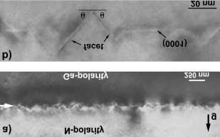
4 of the polarity of the MOCVD substrate, but for sufficiently high Mg exposures (T e = 400 o C) an inversion domain boundary is formed and the polarity of the film is inverted. The incident Mg flux for T Mg = 400 o C is ~ 1 ML/sec and the incorporated Mg concentration (measured by SIMS) is approximately cm -3 in the film where the inversion takes place. These results are consistent with the recent observations by Ramachandran et al for GaN films grown by MBE on SiC(0001) substrates in which a Ga-face to N-face polarity reversal was observed by induced by exposing the film to several monolayers of Mg during growth [5]. High magnification TEM images of the interface indicate that the IDB is faceted as shown in Fig. 3. The dark field image in Fig. 3a is taken along the [1120] axis with a diffraction vector g = (0002). In this image, facets can be observed and complimentary contrast is revealed in the film above and below the interface to confirm the inversion symmetry [8]. The high resolution lattice image in Fig. 3b taken along the [1100] axis shows that the facets contain segments lying in the (0001) plane as well as segments that are inclined with respect to the basal plane. The inclined facets were found to be sharp when imaged in the <1100> projection and diffuse in the <1120> projection. This observation is consistent with the existence of inversion domain boundaries lying in {h,h,-2h,l} planes. In the <1100> projection, the facet angle (θ) ranges from ~ degrees with respect to the basal plane. The existence of Mg-induced (0001) inversion domain boundaries was reported by Ramachandran et al. [5], but {h,h,-2h,l} facets were not observed in that work. A possible atomic model for inversion boundaries lying on the (0001) plane has been discussed elsewhere [5]. We will focus here on the {h,h,-2h,l}facets. As a first step we considered the (1122) plane. An energetically plausible model for an inversion domain boundary lying on this plane may be constructed as shown in Fig 4. In this model all of the N atoms and most of the Ga atoms remain fourfold coordinated as in bulk GaN, but the Ga atoms that are closest to the boundary are each bonded to only three N atoms. In this configuration electrons will occupy the dangling bond (4p z ) orbitals of the Ga atoms. However, by replacing 3 out of 4 Ga atoms by Mg we obtain a configuration in which there is no occupation of the Ga dangling bonds, i.e. such a structure satisfies the electron counting rule. We have performed first principles total energy calculations [10] 4
5 for structural models of (1122) boundaries in which either 0 or ¾ of the threefold Ga atoms are replaced by Mg atoms. The unit cells employed in these calculations contain 4 threefold-coordinated Mg or Ga atoms. The relative energy of these structures depends on the chemical potentials of the atomic constituents; µ Mg, µ Ga, and µ N. For conditions in which there is equilibrium with bulk GaN (µ Ga + µ N = µ GaN(bulk) ) and for which the Mg chemical potential is equal to its maximum possible equilibrium value (3µ Mg + 2µ N = µ Mg3N2(bulk) ), we find that the energy of the (1122) boundary having ¾ Mg occupation is energetically favorable compared to the boundary containing no Mg. The calculated energy difference is ~3.5 ev per unit cell for Ga-rich conditions. This result indicates that the formation energy of such a (1122) inversion domain boundary is reduced significantly under Mg-rich conditions. We have also performed calculations for a boundary lying on the (1123) plane. This plane is inclined by ~ 47 degrees with respect to the basal plane. The structure we considered is indicated in Figure 4. Such a boundary may be described as a mixture of two (1122) segments (P) and a (0001) segment (B), as defined in Figure 4. As for the (1122) boundary, our total energy calculations indicate that the energy of the (1123) boundary is reduced significantly by replacing some of the Ga atoms by Mg atoms. We performed calculations for (1123) boundaries having 6 threefold-coordinated Mg or Ga atoms in each unit cell. We calculate the energy of a structure in which 4 out of 6 Ga atoms are replaced by Mg and compare this with the energy of a structure in which all 6 threefold-coordinated atoms are Ga atoms. [10] For the same conditions on the chemical potentials discussed above, we find that the energy of the Mg-containing structure is lower by 2.75 ev/cell under Ga-rich conditions. On the basis of the calculations for these (1122) and (1123) inversion domain boundaries we propose that the inclined segments of the boundaries observed in the films are Mg-rich, with Mg atoms occupying threefoldcoordinated sites. One may construct inversion domain boundaries inclined at various angles with respect to the basal plane by mixing (1122) and (0001) segments. The (3368) plane, inclined by ~51 degrees, is such a mixture. It contains a mixture of three P-segments and one B-segment as defined in Figure 4. It is possible that the range of inclination angles observed in the TEM images can be accounted for in terms of boundary structures 5
6 consisting of nanometer scale mixtures of (1122) and (0001) segments. The local atomic structure of these boundaries is expected to be similar to those indicated in Figure 4. In summary we have observed that for sufficiently high Mg doping levels the (0001) growth surface of GaN exhibits an instability with respect to polarity inversion, with the formation of a multifaceted IDB. First principles total energy calculations indicate that Mg incorporates in threefold-coordinated binding sites along the facetted segments of the IDB. Since Mg incorporation on the (0001) surface is much less efficient than on the (0001) surface, this Mg-induced polarity inversion may limit the p-type doping levels achievable in MBE grown GaN. The authors are grateful to J.M. Zuo (Arizona State University) for providing the CBED simulations and C.G. Van de Walle for valuable discussions. This work was supported by the Office of Naval Research, Contract No. N C
7 Figure Captions Fig.1. SIMS data showing growth profile and Mg incorporation as a function of depth for a set Mg cell temperatures repeated over two growth cycles at a substrate T s = 710 o C. The second cycle was grown also with hydrogen (H). Fig.2. Convergent beam electron diffraction patterns taken (a) above and (c) below the interface that is indicated by the arrow in (c). (c) is a bright field image taken with a diffraction vector g = 0002 near the [1120] axis of a GaN:Mg film. Fig. 3 (a) High magnification image of the inversion domain boundary (IDB) taken along the [1120] axis with diffraction vector g = (b) Lattice image of the IDB taken along the [1100] axis showing facets that form along the (0001) plane and at an angle θ ~ 50 degrees with the basal plane. Fig. 4 Schematic representations of various possible inversion domain boundaries in GaN. A (1122) boundary is shown on the left. The shaded atoms are threefold coordinated Mg or Ga atoms. Shown on the right is a (1123) boundary comprised of a nanometer scale mixture of (1122) segments (denoted P) and (0001) segments (denoted B). The (1122) and (1123) boundaries are stabilized by replacement of ¾ of the Ga atoms by Mg atoms. The IDB shown here is formed by switching the chemical identity of Ga and N atoms on one side of the boundary, and then performing a translation along the [0001] direction by (5/8) c. 7
8 References 1. S. Nakamura, The blue laser diode: GaN based light emitters and lasers, (Springer, Berlin, 1997). 2. P. Vennegues, M. Benaissa, E. Feltin, P. De Mierry, S. Dalmasso, M. Leroux, and P. Gibart, unpublished 3. Z. Liliental-Weber, M. Benamara, W. Swider, J. Washburn, I. Gregory, S. Porowski, D. J. H. Lambert, C. J. Eiting, and R. D. Dupuis, Appl. Phys. Lett, 75, 4159 (1999) 4. M.D. McCluskey, L.T. Romano, B.S. Krusor, N. M. Johnson, T. Suski, and J. Jun, Appl. Phys. Lett, 73, 1281 (1998) 5. V. Ramachandran, R. M. Feenstra, W. L. Sarney, L. Salamanca-Riba, J. E. Northrup, L. T. Romano, and D. W. Greve, Appl. Phys. Lett, 75, 808 (1999) 6. I.P. Smorchkova, E. Haus, B. Heying, P. Kozodoy, J. P. Ibbetson, S. Keller, S. P. DenBaars, J.S. Speck, and U.K. Mishra, Appl. Phys. Lett, 76, 718, T.H. Myers, A. Ptak, L.T. Romano, J.E. Northrup, C.G. Van de Walle, unpublished 8. L.T. Romano, J. E. Northrup, M. A. O Keefe, Appl. Phys. Lett. 69, 2394 (1996) 9. J.M. Zuo, CBED Simulation Program, Arizona State University 10. R. Stumpf and M. Scheffler, Comput. Phys. Commun. 79, 447 (1994). The plane wave cutoff energy used in these calculations is 40 Ry. 11. The construction of a (1123) boundary structure that satisfies the electron counting rule requires replacement of ¾ of the Ga atoms by Mg. Calculations for such structure would require the use of a unit cell containing 12 threefold atoms. 8
9 Fig. 2
10 Fig. 3
11 P P B P Ga {1122} N (0001) {1123}
12 N Polarity Ga Polarity
TEM Study of the Morphology Of GaN/SiC (0001) Grown at Various Temperatures by MBE
 Grown at Various Temperatures by MBE") TEM Study of the Morphology Of GaN/SiC (0001) Grown at Various Temperatures by MBE W.L. Sarney 1, L. Salamanca-Riba 1, V. Ramachandran 2, R.M Feenstra 2, D.W. Greve 3 1 Dept. of Materials & Nuclear Engineering,
TEM Study of the Morphology Of GaN/SiC (0001) Grown at Various Temperatures by MBE W.L. Sarney 1, L. Salamanca-Riba 1, V. Ramachandran 2, R.M Feenstra 2, D.W. Greve 3 1 Dept. of Materials & Nuclear Engineering,
DISORDERING OF InGaN/GaN SUPERLATTICES AFTER HIGH-PRESSURE ANNEALING
 DISORDERING OF InGaN/GaN SUPERLATTICES AFTER HIGH-PRESSURE ANNEALING M.D. McCluskey*, L.T. Romano**, B.S. Krusor**, D. Hofstetter**, D.P. Bour**, M. Kneissl**, N.M. Johnson**, T. Suski***, J. Jun*** ABSTRACT
In-Situ Characterization During MOVPE Growth of III-Nitrides using Reflectrometry
 18 Annual Report 1999, Dept. of Optoelectronics, University of Ulm In-Situ Characterization During MOVPE Growth of III-Nitrides using Reflectrometry Christoph Kirchner and Matthias Seyboth The suitability
Effects of impurities on the lattice parameters of GaN
 PHYSICAL REVIEW B 68, 165209 2003 Effects of impurities on the lattice parameters of GaN Chris G. Van de Walle* Palo Alto Research Center, 3333 Coyote Hill Road, Palo Alto, California 94304, USA Received
EPITAXY extended single-crystal film formation on top of a crystalline substrate. Homoepitaxy (Si on Si) Heteroepitaxy (AlAs on GaAs)
 Heteroepitaxy (AlAs on GaAs)") extended single-crystal film formation on top of a crystalline substrate Homoepitaxy (Si on Si) Heteroepitaxy (AlAs on GaAs) optoelectronic devices (GaInN) high-frequency wireless communication devices
extended single-crystal film formation on top of a crystalline substrate Homoepitaxy (Si on Si) Heteroepitaxy (AlAs on GaAs) optoelectronic devices (GaInN) high-frequency wireless communication devices
Specimen Preparation Technique for a Microstructure Analysis Using the Focused Ion Beam Process
 Specimen Preparation Technique for a Microstructure Analysis Using the Focused Ion Beam Process by Kozue Yabusaki * and Hirokazu Sasaki * In recent years the FIB technique has been widely used for specimen
Transmission Electron Microscopy (TEM) Prof.Dr.Figen KAYA
 Prof.Dr.Figen KAYA") Transmission Electron Microscopy (TEM) Prof.Dr.Figen KAYA Transmission Electron Microscope A transmission electron microscope, similar to a transmission light microscope, has the following components along
Transmission Electron Microscopy (TEM) Prof.Dr.Figen KAYA Transmission Electron Microscope A transmission electron microscope, similar to a transmission light microscope, has the following components along
TEM imaging and diffraction examples
 TEM imaging and diffraction examples Duncan Alexander EPFL-CIME 1 Diffraction examples Kikuchi diffraction Epitaxial relationships Polycrystalline samples Amorphous materials Contents Convergent beam electron
A CRITICAL COMPARISON BETWEEN MOVPE AND MBE GROWTH OF III-V NITRIDE SEMICONDUCTOR MATERIALS FOR OPTO-ELECTRONIC DEVICE APPLICATIONS
 A CRITICAL COMPARISON BETWEEN MOVPE AND MBE GROWTH OF III-V NITRIDE SEMICONDUCTOR MATERIALS FOR OPTO-ELECTRONIC DEVICE APPLICATIONS M.A.L. JOHNSON,**, ZHONGHAI YU *, J.D. BROWN *, F.A. KOECK *, N.A. EL-MASRY
MOVPE growth of GaN and LED on (1 1 1) MgAl
 MgAl") Journal of Crystal Growth 189/190 (1998) 197 201 MOVPE growth of GaN and LED on (1 1 1) Shukun Duan *, Xuegong Teng, Yutian Wang, Gaohua Li, Hongxing Jiang, Peide Han, Da-Cheng Lu National Integrated Optoelectronics
Journal of Crystal Growth 189/190 (1998) 197 201 MOVPE growth of GaN and LED on (1 1 1) Shukun Duan *, Xuegong Teng, Yutian Wang, Gaohua Li, Hongxing Jiang, Peide Han, Da-Cheng Lu National Integrated Optoelectronics
Practical 2P8 Transmission Electron Microscopy
 Practical 2P8 Transmission Electron Microscopy Originators: Dr. N.P. Young and Prof. J. M. Titchmarsh What you should learn from this practical Science This practical ties-in with the lecture course on
Thin Film Characterizations Using XRD The Cases of VO2 and NbTiN
 Thin Film Characterizations Using XRD The Cases of VO2 and NbTiN A thesis submitted in partial fulfillment of the requirement for the degree of Bachelor of Arts / Science in Physics from The College of
6.8 Magnetic in-plane anisotropy of epitaxially grown Fe-films on vicinal Ag(001) and Au(001) with different miscut orientations
 and Au(001) with different miscut orientations") C. Epitaxial Growth 6.8 Magnetic in-plane anisotropy of epitaxially grown Fe-films on vicinal Ag(001) and Au(001) with different miscut orientations M. Rickart, A.R. Frank, J. Jorzick, Ch. Krämer, S.O.
C. Epitaxial Growth 6.8 Magnetic in-plane anisotropy of epitaxially grown Fe-films on vicinal Ag(001) and Au(001) with different miscut orientations M. Rickart, A.R. Frank, J. Jorzick, Ch. Krämer, S.O.
Kinematical theory of contrast
 Kinematical theory of contrast Image interpretation in the EM the known distribution of the direct and/or diffracted beam on the lower surface of the crystal The image on the screen of an EM = the enlarged
Planar Defects in Materials. Planar Defects in Materials
 Classification of Defects in Solids: Planar defects: Stacking faults o {311} defects in Si o Inversion domain boundaries o Antiphase boundaries (e.g., super dislocations): analogous to partials but in
Defects in Nitride Lasers
 Defects in Nitride Lasers Julita Smalc-Koziorowska Institute of High Pressure Physics UNIPRESS, PAS, Sokolowska 29/37, 01-142 Warsaw, Poland TopGaN Ltd., Sokolowska 29/37, 01-142 Warsaw, Poland Thessaloniki
Twins & Dislocations in HCP Textbook & Paper Reviews. Cindy Smith
 Twins & Dislocations in HCP Textbook & Paper Reviews Cindy Smith Motivation Review: Outline Crystal lattices (fcc, bcc, hcp) Fcc vs. hcp stacking sequences Cubic {hkl} naming Hcp {hkil} naming Twinning
ARTICLE IN PRESS. Journal of Crystal Growth
 Journal of Crystal Growth 312 (2010) 1311 1315 Contents lists available at ScienceDirect Journal of Crystal Growth journal homepage: www.elsevier.com/locate/jcrysgro Abbreviated MOVPE nucleation of III-nitride
InGaN quantum dot based LED for white light emitting
 Emerging Photonics 2014 InGaN quantum dot based LED for white light emitting Luo Yi, Wang Lai, Hao Zhibiao, Han Yanjun, and Li Hongtao Tsinghua National Laboratory for Information Science and Technology,
8. Epitaxy. - Extended single-crystal film formation on top of a crystalline substrate
 8. Epitaxy 1. Introduction επι(epi placed or resting upon) ταξιζ(taxis arrangement) - Extended single-crystal film formation on top of a crystalline substrate - Homoepitaxy : Film and substrate are the
High Temperature Oxygen Out-Diffusion from the Interfacial SiOx Bond Layer in Direct Silicon Bonded (DSB) Substrates
 Substrates") High Temperature Oxygen Out-Diffusion from the Interfacial SiOx Bond Layer in Direct Silicon Bonded (DSB) Substrates Jim Sullivan, Harry R. Kirk, Sien Kang, Philip J. Ong, and Francois J. Henley Silicon
High Temperature Oxygen Out-Diffusion from the Interfacial SiOx Bond Layer in Direct Silicon Bonded (DSB) Substrates Jim Sullivan, Harry R. Kirk, Sien Kang, Philip J. Ong, and Francois J. Henley Silicon
Electron Channeling Contrast Imaging: Rapid Characterization of Semiconductors. Julia I. Deitz 1
 Electron Channeling Contrast Imaging: Rapid Characterization of Semiconductors Julia I. Deitz 1 Introduction For semiconductor technologies, achievement of their ultimate potential depends greatly upon
3.46 OPTICAL AND OPTOELECTRONIC MATERIALS
 Badgap Engineering: Precise Control of Emission Wavelength Wavelength Division Multiplexing Fiber Transmission Window Optical Amplification Spectrum Design and Fabrication of emitters and detectors Composition
Vertical Bridgman growth of sapphire Crystals with thin-neck formation process
 Vertical Bridgman growth of sapphire Crystals with thin-neck formation process K. Hoshikawa 1, T. Taishi 1, E. Ohba 1, 2, C. Miyagawa 1, 2, T. Kobayashi 2, J. Yanagisawa 2, M.Shinozuka 2 Faculty of Engineering,
Electrical, thermal, and microstructural characteristics of TiÕAlÕTiÕAu multilayer Ohmic contacts to n-type GaN
 JOURNAL OF APPLIED PHYSICS VOLUME 93, NUMBER 2 15 JANUARY 2003 Electrical, thermal, and microstructural characteristics of TiÕAlÕTiÕAu multilayer Ohmic contacts to n-type GaN Abhishek Motayed Department
Amorphous Silicon Solar Cells
 The Birnie Group solar class and website were created with much-appreciated support from the NSF CRCD Program under grants 0203504 and 0509886. Continuing Support from the McLaren Endowment is also greatly
J. Jasinski and Z. Liliental-Weber Lawrence Berkeley National Laboratory, Materials Science Division, Berkeley, CA
 Heteroepitaxy of InSe/GaSe on Si(111) Sustrates J. Jasinski and Z. Liliental-Weer Lawrence Berkeley National Laoratory, Materials Science Division, Berkeley, CA A. Chaiken, G.A. Gison, K. Nauka and C.C.
Topological crystalline insulators. Tomasz Story Institute of Physics, Polish Academy of Sciences, Warsaw
 Topological crystalline insulators Tomasz Story Institute of Physics, Polish Academy of Sciences, Warsaw Topological crystalline insulators - outline 1. Introduction topological crystalline insulators
Mg-enhanced lateral overgrowth of GaN on patterned GaN/sapphire substrate by selective Metal Organic Vapor Phase Epitaxy
 M R S Internet Journal Nitride Semiconductor Research Mg-enhanced lateral overgrowth of GaN on patterned GaN/sapphire substrate by selective Metal Organic Vapor Phase Epitaxy B. Beaumont 1, M. Vaille 1,
Molecular Beam Epitaxy Growth of GaAs 1-x Bi x
 Molecular Beam Epitaxy Growth of GaAs 1-x Bi x Dan Beaton, Ryan Lewis, Xianfeng Lu, Mostafa Masnadi-Shirazi, Sebastien Tixier, Erin Young, Martin Adamcyk, UBC, Vancouver, BC B. Fluegel, A. Mascarenhas,
3. Anisotropic blurring by dislocations
 Dynamical Simulation of EBSD Patterns of Imperfect Crystals 1 G. Nolze 1, A. Winkelmann 2 1 Federal Institute for Materials Research and Testing (BAM), Berlin, Germany 2 Max-Planck- Institute of Microstructure
1. Introduction. What is implantation? Advantages
 Ion implantation Contents 1. Introduction 2. Ion range 3. implantation profiles 4. ion channeling 5. ion implantation-induced damage 6. annealing behavior of the damage 7. process consideration 8. comparison
Thin Film Scattering: Epitaxial Layers
 Thin Film Scattering: Epitaxial Layers 6th Annual SSRL Workshop on Synchrotron X-ray Scattering Techniques in Materials and Environmental Sciences: Theory and Application May 29-31, 2012 Thin films. Epitaxial
Simple method for formation of nanometer scale holes in membranes. E. O. Lawrence Berkeley National Laboratory, Berkeley, CA 94720
 Simple method for formation of nanometer scale holes in membranes T. Schenkel 1, E. A. Stach, V. Radmilovic, S.-J. Park, and A. Persaud E. O. Lawrence Berkeley National Laboratory, Berkeley, CA 94720 When
J.H. Edgar, Z. Gu, and K. Taggart, Kansas State University, Department of Chemical Engineering, Durland Hall, Manhattan, KS
 Mater. Res. Soc. Symp. Proc. Vol. 892 2006 Materials Research Society 0892-FF21-02.1 Oxidation of Aluminum Nitride for Defect Characterization J.H. Edgar, Z. Gu, and K. Taggart, Kansas State University,
BLUE AND UV SEMICONDUCTOR LASERS
 Vol. 37 (2006) ACTA PHYSICA POLONICA B No 4 BLUE AND UV SEMICONDUCTOR LASERS S. Krukowski, C. Skierbiszewski, P. Perlin, M. Leszczynski, M. Bockowski, S. Porowski Institute of High Pressure Physics, Polish
INVESTIGATION OF ANTIPHASE DOMAIN BOUNDARY ENERGETICS IN GAAS-ON-SI(001)
") INVESTIGATION OF ANTIPHASE DOMAIN BOUNDARY ENERGETICS IN GAAS-ON-SI(001) By CALEB SHUAN CHIA BARRETT A DISSERTATION PRESENTED TO THE GRADUATE SCHOOL OF THE UNIVERSITY OF FLORIDA IN PARTIAL FULFILLMENT
INVESTIGATION OF ANTIPHASE DOMAIN BOUNDARY ENERGETICS IN GAAS-ON-SI(001) By CALEB SHUAN CHIA BARRETT A DISSERTATION PRESENTED TO THE GRADUATE SCHOOL OF THE UNIVERSITY OF FLORIDA IN PARTIAL FULFILLMENT
Structure and optical properties of M/ZnO (M=Au, Cu, Pt) nanocomposites
 nanocomposites") Solar Energy Materials & Solar Cells 8 () 339 38 Structure and optical properties of M/ (M=Au, Cu, Pt) nanocomposites U. Pal a,b, *, J. Garc!ıa-Serrano a, G. Casarrubias-Segura a, N. Koshizaki c, T. Sasaki
Solar Energy Materials & Solar Cells 8 () 339 38 Structure and optical properties of M/ (M=Au, Cu, Pt) nanocomposites U. Pal a,b, *, J. Garc!ıa-Serrano a, G. Casarrubias-Segura a, N. Koshizaki c, T. Sasaki
Investigation of wurtzite (B,Al)N films prepared on polycrystalline diamond
N films prepared on polycrystalline diamond") Available online at www.sciencedirect.com Thin Solid Films 516 (2007) 223 227 www.elsevier.com/locate/tsf Investigation of wurtzite (B,Al)N films prepared on polycrystalline diamond J.H. Song a, J.L. Huang
Available online at www.sciencedirect.com Thin Solid Films 516 (2007) 223 227 www.elsevier.com/locate/tsf Investigation of wurtzite (B,Al)N films prepared on polycrystalline diamond J.H. Song a, J.L. Huang
Single Crystal Growth of Aluminum Nitride
 Single Crystal Growth of Aluminum Nitride Hiroyuki Kamata 1, Yuu Ishii 2, Toshiaki Mabuchi 3, Kunihiro Naoe 1, Shoji Ajimura 4, Kazuo Sanada 5 Single crystalline aluminum nitride (AlN) is a promising material
Deformation Twinning in Bulk Aluminum with Coarse Grains
 Proceedings of the 12th International Conference on Aluminium Proceedings Alloys, of the September 12th International 5-9, 2010, Yokohama, Conference Japan on 2010 Aluminum The Japan Alloys, Institute
Ferroelectric Oxide Single-Crystalline Layers by Wafer Bonding and Hydrogen/Helium Implantation
 Mat. Res. Soc. Symp. Proc. Vol. 748 2003 Materials Research Society U11.8.1 Ferroelectric Oxide Single-Crystalline Layers by Wafer Bonding and Hydrogen/Helium Implantation Ionut Radu, Izabela Szafraniak,
Electron microscopy II
 Electron microscopy II Nanomaterials characterization I RNDr. Věra Vodičková, PhD. Interaction ction: electrons solid matter Signal types SE.secondary e - AE Auger s e - BSE back scattered e - X-ray photons,
Journal of Crystal Growth
 Journal of Crystal Growth 323 (2011) 127 131 Contents lists available at ScienceDirect Journal of Crystal Growth journal homepage: www.elsevier.com/locate/jcrysgro Growth and material properties of ZnTe
Light enhancement by the formation of an Al-oxide honeycomb nano-structure on the n-gan surface of thin-gan light-emitting diodes
 Light enhancement by the formation of an Al-oxide honeycomb nano-structure on the n-gan surface of thin-gan light-emitting diodes C. L. Lin, P. H. Chen Department of Chemical and Materials Engineering,
Introduction Joachim Piprek
 3 1 Introduction Joachim Piprek 1.1 A Brief History Considerable efforts to fabricate nitride devices began more than three decades ago. In 1971, Pankove et al. reported the first GaN-based lightemitting
SEMIPOLAR GaN ON Si(001): THE ROLE OF SiC BUFFER LAYER SYNTHESIZED BY METHOD OF SUBSTRATE ATOM SUBSTITUTION
: THE ROLE OF SiC BUFFER LAYER SYNTHESIZED BY METHOD OF SUBSTRATE ATOM SUBSTITUTION") Materials Physics and Mechanics 21 (2014) 71-77 Received: June 15, 2014 SEMIPOLAR GaN ON Si(001): THE ROLE OF SiC BUFFER LAYER SYNTHESIZED BY METHOD OF SUBSTRATE ATOM SUBSTITUTION V.N. Bessolov 1, E.V.
Materials Physics and Mechanics 21 (2014) 71-77 Received: June 15, 2014 SEMIPOLAR GaN ON Si(001): THE ROLE OF SiC BUFFER LAYER SYNTHESIZED BY METHOD OF SUBSTRATE ATOM SUBSTITUTION V.N. Bessolov 1, E.V.
The Role of Physical Defects in Electrical Degradation of GaN HEMTs
 The Role of Physical Defects in Electrical Degradation of GaN HEMTs Carl V. Thompson Dept. of Materials Science and Engineering, MIT Faculty Collaborators: Chee Lip Gan 2,3, Tomas Palacios 1, Jesus Del
Specimen configuration
 APPLICATIONNOTE Model 1040 NanoMill TEM specimen preparation system Specimen configuration Preparing focused ion beam (FIB) milled specimens for submission to Fischione Instruments. The Model 1040 NanoMill
Annealing Effect on Elastic Constant of Ultrathin Films Studied by Acoustic-Phonon Resonance Spectroscopy
 1st International Symposium on Laser Ultrasonics: Science, Technology and Applications July 16-18 28, Montreal, Canada Annealing Effect on Elastic Constant of Ultrathin Films Studied by Acoustic-Phonon
Preparation and Characterization of Micro-Crystalline Hydrogenated Silicon Carbide p-layers
 Preparation and Characterization of Micro-Crystalline Hydrogenated Silicon Carbide p-layers Erten Eser, Steven S. Hegedus and Wayne A. Buchanan Institute of Energy Conversion University of Delaware, Newark,
Point Defects. Vacancies are the most important form. Vacancies Self-interstitials
 Grain Boundaries 1 Point Defects 2 Point Defects A Point Defect is a crystalline defect associated with one or, at most, several atomic sites. These are defects at a single atom position. Vacancies Self-interstitials
STRUCTURE AND MORPHOLOGY OF INDIUM NITRIDE THIN FILMS GROWN BY PLASMA ASSISTED PLD: THE IMPACT OF NITROGEN FLOW AND SUBSTRATE TEMPERATURE
 Romanian Reports in Physics, Vol. 65, No. 1, P. 213 218, 2013 PLASMA PHYSICS STRUCTURE AND MORPHOLOGY OF INDIUM NITRIDE THIN FILMS GROWN BY PLASMA ASSISTED PLD: THE IMPACT OF NITROGEN FLOW AND SUBSTRATE
Transmission Mode Photocathodes Covering the Spectral Range
 Transmission Mode Photocathodes Covering the Spectral Range 6/19/2002 New Developments in Photodetection 3 rd Beaune Conference June 17-21, 2002 Arlynn Smith, Keith Passmore, Roger Sillmon, Rudy Benz ITT
JECP/HOLZ, an Interactive Computer Program for Simulation of HOLZ Pattern
 JECP/HOLZ, an Interactive Computer Program for Simulation of HOLZ Pattern (Version 2t) X.Z. Li, Ph. D Copyright(C) 2002-2017 LANDYNE All Rights Reserved. Contents: 1. Purpose of the program 2. Graphic
Measurement of Residual Stress by X-ray Diffraction
 Measurement of Residual Stress by X-ray Diffraction C-563 Overview Definitions Origin Methods of determination of residual stresses Method of X-ray diffraction (details) References End Stress and Strain
Figure 2.3 (cont., p. 60) (e) Block diagram of Pentium 4 processor with 42 million transistors (2000). [Courtesy Intel Corporation.
 (e) Block diagram of Pentium 4 processor with 42 million transistors (2000). [Courtesy Intel Corporation.") Figure 2.1 (p. 58) Basic fabrication steps in the silicon planar process: (a) oxide formation, (b) selective oxide removal, (c) deposition of dopant atoms on wafer, (d) diffusion of dopant atoms into exposed
Figure 2.1 (p. 58) Basic fabrication steps in the silicon planar process: (a) oxide formation, (b) selective oxide removal, (c) deposition of dopant atoms on wafer, (d) diffusion of dopant atoms into exposed
HIGH-EFFICIENCY DILUTE NITRIDE MULTIJUNCTION SOLAR CELLS: INFLUENCE OF POINT DEFECTS ON THE DEVICE PERFORMANCE
 HIGH-EFFICIENCY DILUTE NITRIDE MULTIJUNCTION SOLAR CELLS: INFLUENCE OF POINT DEFECTS ON THE DEVICE PERFORMANCE Ville Polojärvi, Arto Aho, Antti Tukiainen, Marianna Raappana, Timo Aho, Mircea Guina Optoelectronics
Hybrid magnetic/semiconductor spintronic materials and devices
 Journal of Magnetism and Magnetic Materials 00 (2006) 000--000 Hybrid magnetic/semiconductor spintronic materials and devices Y.B. Xu, E. Ahmad, J. S. Claydon, Y.X. Lu, S. S. A. Hassan, I. G. Will and
Characterisation of multiple carrier transport in indium nitride grown by molecular beam epitaxy
 phys. stat. sol. (c) 4, No. 7, 2423 2427 (2007) / DOI 10.1002/pssc.200674780 Characterisation of multiple carrier transport in indium nitride grown by molecular beam epitaxy Tamara B. Fehlberg 1, Gilberto
Structure Analysis of -phase in Sb-Te Alloys by HRTEM* 1
 Materials Transactions, Vol. 45, No. 8 (2004) pp. 2673 to 2677 #2004 The Japan Institute of Metals Structure Analysis of -phase in Sb-Te Alloys by HRTEM* 1 Yoshiyuki Nakata 1, Takehito Suenaga 1; * 2,
Band-gap Engineering in Sputter Deposited Amorphous/Microcrystalline Sc x Ga 1-x N
 NASA/CR-2001-211241 ICASE Report No. 2001-36 Band-gap Engineering in Sputter Deposited Amorphous/Microcrystalline Sc x Ga 1-x N Mark E. Little ICASE, Hampton, Virginia Martin E. Kordesch Ohio University,
2014 the Nobel Prize in Physics Awarded to Isamu Akasaki
 Awarded Awarded to Isamu Akasaki Isamu Akasaki ( 赤崎勇 ) was born in Kagoshima, Japan. Dr. Akasaki graduated from Kyoto University in 1952, and obtained a Ph.D degree in Electronics from Nagoya University
VLSI Technology. By: Ajay Kumar Gautam
 By: Ajay Kumar Gautam Introduction to VLSI Technology, Crystal Growth, Oxidation, Epitaxial Process, Diffusion Process, Ion Implantation, Lithography, Etching, Metallization, VLSI Process Integration,
Metallization deposition and etching. Material mainly taken from Campbell, UCCS
 Metallization deposition and etching Material mainly taken from Campbell, UCCS Application Metallization is back-end processing Metals used are aluminum and copper Mainly involves deposition and etching,
Sublimation growth of thick freestanding 3C- SiC using CVD-templates on silicon as seeds
 Sublimation growth of thick freestanding 3C- SiC using CVD-templates on silicon as seeds Philip Hens, Valdas Jokubavicius, Rickard Liljedahl, G Wagner, Rositsa Yakimova, P Wellmann and Mikael Syväjärvi
Studies on Si-doped AlGaN Epilayers
 Studies on Si-doped AlGaN Epilayers 47 Studies on Si-doped AlGaN Epilayers Kamran Forghani Growth optimization of Si doped AlGaN epilayers with 20%, 30% and 45%Al content grown on AlGaN-sapphire by MOVPE
Heavily Aluminum-Doped Epitaxial Layers for Ohmic Contact Formation to p-type 4H-SiC Produced by Low-Temperature Homoepitaxial Growth
 Journal of ELECTRONIC MATERIALS, Vol. 39, No. 1, 2010 DOI: 10.1007/s11664-009-0953-6 Ó 2009 TMS Heavily Aluminum-Doped Epitaxial Layers for Ohmic Contact Formation to p-type 4H-SiC Produced by Low-Temperature
Boron Diffusion and Silicon Self-Interstitial Recycling between SiGeC layers
 Mat. Res. Soc. Symp. Proc. Vol. 810 2004 Materials Research Society C3.5.1 oron Diffusion and Silicon Self-Interstitial Recycling between SiGeC layers M. S. Carroll 1 J. C. Sturm, Dept. of Electrical Engineering,
The atomic and electronic structure of dislocations in Ga based nitride semiconductors
 The atomic and electronic structure of dislocations in Ga based nitride semiconductors Imad Belabbas, Pierre Ruterana, Jun Chen, Gérard Nouet To cite this version: Imad Belabbas, Pierre Ruterana, Jun Chen,
Chapter Outline How do atoms arrange themselves to form solids?
 Chapter Outline How do atoms arrange themselves to form solids? Fundamental concepts and language Unit cells Crystal structures Face-centered cubic Body-centered cubic Hexagonal close-packed Close packed
Highly selective photoenhanced wet etching of GaN for defect investigation and device fabrication
 Mat. Res. Soc. Symp. Proc. Vol. 639 2001 Materials Research Society Highly selective photoenhanced wet etching of GaN for defect investigation and device fabrication P. Visconti 1, M. A. Reshchikov, K.
The Significance of Bragg s Law in Electron Diffraction and Microscopy and Bragg s Second Law
 The Significance of Bragg s Law in Electron Diffraction and Microscopy and Bragg s Second Law Colin Humphreys University of Cambridge Bragg Symposium Adelaide 6 December 2012 Bragg s Second Law E. W.
Radiation Tolerant Isolation Technology
 Radiation Tolerant Isolation Technology Background The following contains a brief description of isolation technologies used for radiation hardened integrated circuits. The technologies mentioned are junction
350 C for 8 hours in argon atmosphere. Supplementary Figures. Supplementary Figure 1 High-temperature annealing of BP flakes on SiO 2.
 Supplementary Figures Supplementary Figure 1 High-temperature annealing of BP flakes on SiO 2. (a-d) The optical images of three BP flakes on a SiO 2 substrate before (a,b) and after annealing (c,d) at
Lecture 12. Physical Vapor Deposition: Evaporation and Sputtering Reading: Chapter 12. ECE Dr. Alan Doolittle
 Lecture 12 Physical Vapor Deposition: Evaporation and Sputtering Reading: Chapter 12 Evaporation and Sputtering (Metalization) Evaporation For all devices, there is a need to go from semiconductor to metal.
Enhanced magneto-optical effect due to interface alloy formation in Co±Pt (1 1 1) ultrathin lms upon thermal annealing
 ultrathin lms upon thermal annealing") Applied Surface Science 169±170 (2001) 231±235 Enhanced magneto-optical effect due to interface alloy formation in Co±Pt (1 1 1) ultrathin lms upon thermal annealing M.-T. Lin a,*, C.C. Kuo a, J.W. Ho
Applied Surface Science 169±170 (2001) 231±235 Enhanced magneto-optical effect due to interface alloy formation in Co±Pt (1 1 1) ultrathin lms upon thermal annealing M.-T. Lin a,*, C.C. Kuo a, J.W. Ho
Chemical analysis of Ti/Al/Ni/Au ohmic contacts to AlGaN/GaN heterostructures
 Optica Applicata, Vol. XLIII, No. 1, 213 DOI: 1.277/oa1319 Chemical analysis of Ti/Al/Ni/Au ohmic contacts to AlGaN/GaN heterostructures WOJCIECH MACHERZYŃSKI *, KORNELIA INDYKIEWICZ, BOGDAN PASZKIEWICZ
Gallium Nitride: An Overview of Structural Defects
 4 Gallium Nitride: An Overview of Structural Defects Fong Kwong Yam, Li Li Low, Sue Ann Oh and Zainuriah Hassan School of Physics, Universiti Sains Malaysia, Malaysia 1. Introduction 1.1 Foreword The III-V
Introduction to Dislocation Mechanics
 Introduction to Dislocation Mechanics What is Dislocation Mechanics? (as meant here) The study of the stress state and deformation of continua whose elastic response is mediated by the nucleation, presence,
This journal is The Royal Society of Chemistry S 1
 2013 S 1 Thermochemical analysis on the growth of NiAl 2 O 4 rods Sang Sub Kim, a Yong Jung Kwon, b Gunju Sun, a Hyoun Woo Kim,* b and Ping Wu* c a Department of Materials Science and Engineering, Inha
Ion channeling effects on the focused ion beam milling of Cu
 Ion channeling effects on the focused ion beam milling of Cu B. W. Kempshall a) and S. M. Schwarz Department of Mechanical, Materials, and Aerospace Engineering, University of Central Florida, P.O. Box
Some Aspects of Sublimation Growth of SiC Ingots p. 41 Growth of Highly Aluminum-Doped p-type 6H-SiC Single Crystals by the Modified Lely Method
 SiC Bulk Growth Large Diameter, Low Defect Silicon Carbide Boule Growth p. 3 SiC Single Crystal Growth by Sublimation: Experimental and Numerical Results p. 7 Impact of SiC Source Material on Temperature
Growth of YBa 2 Cu 3 O 7 Films with [110] Tilt of CuO Planes to Surface on SrTiO 3 Crystals
![Growth of YBa 2 Cu 3 O 7 Films with [110] Tilt of CuO Planes to Surface on SrTiO 3 Crystals](/thumbs/72/67895252.jpg "Growth of YBa 2 Cu 3 O 7 Films with [110] Tilt of CuO Planes to Surface on SrTiO 3 Crystals") ISSN 163-7745, Crystallography Reports, 213, Vol. 58, No. 3, pp. 488 492. Pleiades Publishing, Inc., 213. Original Russian Text E.A. Stepantsov, F. Lombardi, D. Winkler, 213, published in Kristallografiya,
ISSN 163-7745, Crystallography Reports, 213, Vol. 58, No. 3, pp. 488 492. Pleiades Publishing, Inc., 213. Original Russian Text E.A. Stepantsov, F. Lombardi, D. Winkler, 213, published in Kristallografiya,
Suitable Semiconductor Properties for Photoelectrochemistry Evaluated using Nitrides
 Univ. Jaume-I Castellon de la Plana, Spain, 2012.09.18 1 Suitable Semiconductor Properties for Photoelectrochemistry Evaluated using Nitrides Katsushi Fujii Global Solar and Initiative : GS + I, the University
Surface Analysis of Electrochromic Switchable Mirror Glass Based on Magnesium-Nickel Thin Film in Accelerated Degradation Test
 Materials Transactions, Vol. 52, No. 3 (2011) pp. 464 to 468 #2011 The Japan Institute of Metals Surface Analysis of Electrochromic Switchable Mirror Glass Based on Magnesium-Nickel Thin Film in Accelerated
4 Concept of Ripple Pyrometry during Flash Lamp Annealing
 4 Concept of Ripple Pyrometry during Flash Lamp Annealing 4.1 Review on Temperature Measurement for Flash Lamp Annealing Several different efforts have been undertaken to measure temperature by contactless
Microstructural study of titanium carbide coating on cemented carbide
 JOURNAL OF MATERIALS SCIENCE 17 (1982) 589-594 Microstructural study of titanium carbide coating on cemented carbide S. VUORINEN, A. HORSEWELL* Laboratory of Applied Physics I, Technical University of
Three-dimensional epitaxy: Thermodynamic stability range of coherent germanium nanocrystallites in silicon
 Three-dimensional epitaxy: Thermodynamic stability range of coherent germanium nanocrystallites in silicon S. Balasubramanian, a) G. Ceder, and K. D. Kolenbrander Department of Materials Science and Engineering,
Transmission Kikuchi Diffraction in the Scanning Electron Microscope
 Transmission Kikuchi Diffraction in the Scanning Electron Microscope Robert Keller, Roy Geiss, Katherine Rice National Institute of Standards and Technology Nanoscale Reliability Group Boulder, Colorado
Performance at Wafer-Scale
 Supporting Information Self-Assembling VO 2 Nanonet with High Switching Performance at Wafer-Scale Jiasong Zhang, Haibo Jin*, Zhuo Chen, Maosheng Cao, Pengwan Chen, Yankun Dou, Yongjie Zhao, Jingbo Li*
Croissance et propriétés magnétiques de réseaux planaires auto-organisés de nanofils de Fer
 Croissance et propriétés magnétiques de réseaux planaires auto-organisés de nanofils de Fer B. Borca, O.Fruchart, M. Hasegawa, C. Meyer Laboratoire Louis Néel (CNRS-UJF-INPG) Grenoble Olivier Fruchart
High-efficiency GaN-based light-emitting diodes fabricated with identical Ag contact formed on both n- and p-layers
 High-efficiency GaN-based light-emitting diodes fabricated with identical Ag contact formed on both n- and p-layers Munsik Oh and Hyunsoo Kim * School of Semiconductor and Chemical Engineering and Semiconductor
MOCVD Growth of GaBN on 6H-SiC (0001) Substrates
 Substrates") 452 Journal of ELECTRONIC MATERIALS, Vol. 29, No. 4, 2000 Chaudhuri, Ignatiev, Regular and Issue Braski Paper MOCVD Growth of GaBN on 6H-SiC (0001) Substrates C.H. WEI, 1 Z.Y. XIE, 1 J.H. EDGAR, 1 K.C.
452 Journal of ELECTRONIC MATERIALS, Vol. 29, No. 4, 2000 Chaudhuri, Ignatiev, Regular and Issue Braski Paper MOCVD Growth of GaBN on 6H-SiC (0001) Substrates C.H. WEI, 1 Z.Y. XIE, 1 J.H. EDGAR, 1 K.C.
Oxide Growth. 1. Introduction
 Oxide Growth 1. Introduction Development of high-quality silicon dioxide (SiO2) has helped to establish the dominance of silicon in the production of commercial integrated circuits. Among all the various
Isolation Technology. Dr. Lynn Fuller
 ROCHESTER INSTITUTE OF TECHNOLOGY MICROELECTRONIC ENGINEERING Isolation Technology Dr. Lynn Fuller Motorola Professor 82 Lomb Memorial Drive Rochester, NY 14623-5604 Tel (585) 475-2035 Fax (585) 475-5041
A Phase Field Model for Grain Growth and Thermal Grooving in Thin Films with Orientation Dependent Surface Energy
 Solid State Phenomena Vol. 129 (2007) pp. 89-94 online at http://www.scientific.net (2007) Trans Tech Publications, Switzerland A Phase Field Model for Grain Growth and Thermal Grooving in Thin Films with
Atomic Structure of Ultrathin Gold Nanowires
 Supporting Information For Atomic Structure of Ultrathin Gold Nanowires Yi Yu, 1,2 Fan Cui, 1,2 Jianwei Sun, 1,2 and Peidong Yang* 1,2,3,4 1 Department of Chemistry, University of California, Berkeley,
Combinatorial RF Magnetron Sputtering for Rapid Materials Discovery: Methodology and Applications
 Combinatorial RF Magnetron Sputtering for Rapid Materials Discovery: Methodology and Applications Philip D. Rack,, Jason D. Fowlkes, and Yuepeng Deng Department of Materials Science and Engineering University
The effect of ion milling on the morphology of ramp-type Josephson junctions
 Journal of MATERIALS RESEARCH Welcome Comments Help The effect of ion milling on the morphology of ramp-type Josephson junctions Dave H. A. Blank and Horst Rogalla Low Temperature Division, Department