Surface Micromachining II
|
|
|
- Aileen Stevens
- 6 years ago
- Views:
Transcription

1 Surface Micromachining II Dr. Thara Srinivasan Lecture 4 Picture credit: Sandia National Lab Lecture Outline Reading From reader: Bustillo, J. et al., Surface Micromachining of Microelectromechanical Systems, pp , Problem set #1 due; problem set #2 on website Today s Lecture Lateral Resonator Process Flow (from Lecture 3) MUMPS Foundry and Design Rules Sandia and Texas Instruments Processes MEMS Test Structures Microstructure Release and Surface Passivation 2

2 Lateral Resonator Process Flow electrostatic comb drive bumper shuttle spring suspension Shuttle with attached combs are spring-suspended 2 µm above ground plane poly 3 Lecture Outline Today s Lecture Lateral Resonator Process Flow MUMPS Foundry and Design Rules Sandia and Texas Instruments Processes MEMS Test Structures Microstructure Release and Surface Passivation 4


3 MultiUser MEMS Process Microelectronics Center of North Carolina, MultiUser MEMS Process (MUMPS), now owned by MEMSCAP, France. Three-level polysi surface micromachining prototyping and foundry service 8 photomasks $4,900 for 1 cm 2 die area 5 MUMPS Micromotor 6


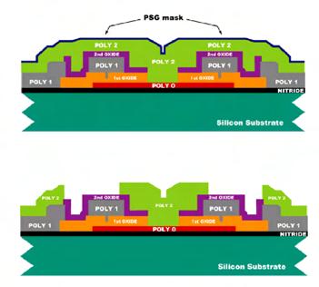
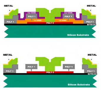
4 MUMPS Process Flow I 7 MUMPS Process Flow II 8


5 MUMPS Process Layers Layer properties Thickness Stress 9 MUMPS Masks Mask conventions Light field: draw features that will stay through fabrication Dark field: draw holes to be cut out 10
,")


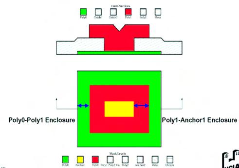
6 MUMPS Minimum Features Minimum feature size Determined by MUMPS photolithography precision Violations results in missing (unanchored), under/oversized, or fused features Use minimum feature only when absolutely necessary nominal min feature min space poly0, 1, 2, hole0, poly1_poly2_via 3 µm 2 2 anchor1, dimple metal hole1, hole holem A. Enclosure B. Spacing MUMPS Design Rules C. Cut-in D. Cut-out 12

7 Design Rule Summary 13 Design Rule Example 14

8 Design Rule Example 15 Stringers and Planarization Sidewall stringers Planarization 16


9 Lecture Outline Today s Lecture Lateral Resonator Process Flow MUMPS Foundry and Design Rules Sandia and Texas Instruments Processes MEMS Test Structures Microstructure Release and Surface Passivation 17 Sandia SUMMiT Process 1 mechanical layer 2 mechanical layers 3 mechanical layers 18


10 Sandia SUMMIT Process Sandia Ultraplanar Multilevel MEMS Technology (SUMMiT) is a 5-layer polysilicon process 14 masks, up to 240 process steps; most complex poly surface micromachining process 1 ground plane/electrical interconnect layer 4 mechanical layers Residual film stress < 5 MPa Device topography is planarized using chemicalmechanical polishing (CMP) 4-poly process stack 19 SUMMIT Devices Comb drive microengine actuates hinged mirror through gear transmission 20


11 Digital Micromirror Display Texas Instruments DMD 2-D array of optical switching pixels on silicon substrate. Pixel is a reflective micromirror supported on a central post Post is mounted on lower metal platform, yoke, suspended by torsional hinges from posts anchored to substrate. 2 electrodes under yoke are used to tilt mirror ±10 Component in >17 projector brands 21 Digital Micromirror Display 16 µm 22

12 DMD Fabrication Maluf 23 Lecture Outline Today s Lecture Lateral Resonator Process Flow MUMPS Foundry and Design Rules Sandia and Texas Instruments Processes MEMS Test Structures Microstructure Release and Surface Passivation 24

13 Thin Films Mechanical Properties Mechanical properties which are critical Adhesion Residual stress, σ Stress gradient, Γ Pinhole density Density Mechanical strength Young s modulus, Ε Fracture strength Fatigue Need for on-wafer measurement Local measurement of film properties Difficult to handle and align small structures 25 Residual Stress Origins of residual stress, σ Growth processes Non-equilibrium deposition Grain morphology change Gas entrapment Doping Thermal stresses Deposition, Coefficient of thermal expansion mismatch Annealing Stress gradient Variation of residual stress in the direction of film growth Can warp released structures in z-direction A bad day at MCNC! (1996) 26

 Compressive stress causes buckling Arrays with increasing length are")
14 Stress Measurement Wafer curvature method (Tencor Flexus) Compressive stress makes wafer convex, tensile stress makes wafer concave. Optically measure deflection of wafer before and after film is deposited σ = E T 2 6Rt 27 MEMS Test Structure: Stress Clamped-clamped beams (bridges) Compressive stress causes buckling Arrays with increasing length are used to determine critical buckling load Only compressive stress is measurable EI σ cr 2 L 28


![down Assuming linear Γ [L -1 ], z = ΓL 2 / 2 L.S.](/docs-images/77/74548166/images/15-4.jpg "Fan Ph.D. Spiral cantilevers Krulevitch Ph.D. + compressive tensile 30")
15 MEMS Test Structure: Stress Vernier pointers Expansion or contraction of beams causes deflection of pointer, read on vernier Single structure indicates compressive or tensile stress 29 Stress Gradient Measurement Beam cantilevers Strain gradient Γ causes beams to deflect up or down Assuming linear Γ [L -1 ], z = ΓL 2 / 2 L.S. Fan Ph.D. Spiral cantilevers Krulevitch Ph.D. + compressive tensile 30
![Young s Modulus Definition: slope of stress-strain curve in elastic region [N/m² = Pa] σ = Eε ε = L / L Silicon (ave.](/docs-images/77/74548166/images/16-1.jpg ") Silicon nitride Silicon dioxide Polysilicon 160 GPa 323 GPa 73 GPa 140-190 GPa On-chip measurement Resonating structures f 0 1 2π 4E tw")
 Fracture surface examined using SEM test beams folded flexure structure P.T.")
16 Young s Modulus Definition: slope of stress-strain curve in elastic region [N/m² = Pa] σ = Eε ε = L / L Silicon (ave.) Silicon nitride Silicon dioxide Polysilicon 160 GPa 323 GPa 73 GPa GPa On-chip measurement Resonating structures f 0 1 2π 4E tw y ML MEMS Test Structure: Fracture Fracture testing by beam bending Test structure shuttle pushed by probe tip so test beams hit and push against bumpers Fracture limit is 1-3 GPa (2.8 GPa) Fracture surface examined using SEM test beams folded flexure structure P.T.Jones PhD vernier shuttle 32

17 MEMS Test Structure: Fatigue Fatigue testing Microdevice with notched flexure resonated until stiffness change measured C. Muhlstein et al. 33 Variations in Microstructure Dimensions Sources of variation: Lithography-to-etch variation Non-vertical sidewalls; trapezoidal cross sections Tolerance ± 5% (±0.1 µm for t = W = 2 µm) Resulting Resonant Frequency Variation f (W/L) 3/2, σ negligible f = 15% for W = 2 µm f (W/L) 1/2, σ dominant f = 5% Compensation Laser trimming Isotropic etch Electrical tuning 34


18 Lecture Outline Today s Lecture Lateral Resonator Process Flow MEMS Test Structures Foundries and Design Rules TI s Digital Micromirror Display Process Flow Microstructure Release and Surface Passivation 35 Microstructure Release and Stiction Stiction ~ the unintended sticking of MEMS surfaces Release stiction ~ While drying after release etch, capillary forces of droplets pull surfaces into contact leading to permanent sticking In-use stiction ~ During device use, surfaces may come into contact and adhere due to Capillary condensation Electrostatic forces Hydrogen bonding van der Waals forces CJ Kim et al. 36

 P solid liquid STP Sublimation Supercritical")

19 Avoiding Stiction Reducing droplet area with mechanical approaches ~ standoff bumps, meniscus-shaping features and tethers Avoiding liquid-vapor meniscus formation completely Supercritical CO 2, sublimated solvents Vapor-phase sacrificial layer etch Surface modification to change meniscus shape from concave to convex Teflon-like films Hydrophobic self-assembled monolayers (SAMs) P solid liquid STP Sublimation Supercritical drying Critical point Evaporation vapor T 37 Dry Release Dry sacrificial layer etches Etch sacrificial oxide with HF vapor Etch sacrificial polymer layer using O 2 plasma Spin-on polymer spacer, etch with plasma CJ Kim et al. Kobayashi et al. 38


20 CO 2 Supercritical Drying Release with supercritical CO 2 Supercritical phase avoids liquidvapor meniscus Procedure HF etching of oxide Thorough water rinses Methanol rinses and soaks, then put wafer into chamber Liquid CO 2 displaces methanol CO 2 goes from liquid to supercritical to gas P solid liquid Supercritical drying Critical point Mulhern et al. STP vapor T 39 Hydrophilic, Hydrophobic Hydrophilic, θ water < 90 Hydrophobic, θ water > θ 3 contact angle Hydrophilic case P 2 d Lotus surface, Univ. Mainz Hydrophobic case P 1 P 1 P 2 40
17SiCl3 3 contact angle Substrate θwater ODT SAM 112 ± 0.")

21 Self-Assembled Monolayers SAMs as nonstick coatings Conformal, ultrathin Low surface energy Covalently bound wear resistant Thermally stable θ 1 Substrate OTS 2 CH3(CH2)17SiCl3 3 contact angle Substrate θwater ODT SAM 112 ± 0.7 SiO2 <10 41 Adhesion Test Structures Cantilever beam array Electrostatically actuated Beam length that remains stuck after voltage turned off determines adhesion energy between surfaces Clamped-clamped beams anchor actuation pad beam landing pad 2 µm ground-plane polysilicon Si substrate voltage on 42 21

 Coefficient of friction results from MEMS test structures friction-testing microstructures and rotating gears plain polysi (oxide-coated) µ s = 4.9 ± 1.2, µ k 0.26-0.")
22 Friction in MEMS Friction between MEMS surfaces Consumes significant portion of motive force Dominant failure mode is intermittent sticking followed by seizure Results in wear at contacting surfaces beam y post beam x Friction test structures Srinivasan, Howe, Maboudian et al.... equilibrium position... displaced and clamped 43 Stiction, Friction Reduction Stiction results With OTS self-assembled monolayer or Teflon coating Can release extremely compliant beams (up to 2 mm long, 2 µm thick, 10 µm wide for SAM) Coefficient of friction results from MEMS test structures friction-testing microstructures and rotating gears plain polysi (oxide-coated) µ s = 4.9 ± 1.2, µ k OTS self-assembled monolayer µ s = 0.09 ± 0.01, µ k = 0.07 ± 0.01 Teflon-coated polysilicon µ k Sandia friction tester: 350 longer until device seizure Texas Instruments DMD: mean time to failure 100,000 h 44
Regents of the University of California
 Surface-Micromachining Process Flow Photoresist Sacrificial Oxide Structural Polysilcon Deposit sacrificial PSG: Target = 2 m 1 hr. 40 min. LPCVD @450 o C Densify the PSG Anneal @950 o C for 30 min. Lithography
EE C245 ME C218 Introduction to MEMS Design Fall 2011
 Lecture Outline EE C245 ME C218 Introduction to MEMS Design Fall 2011 Prof. Clark T.-C. Nguyen Dept. of Electrical Engineering & Computer Sciences University of California at Berkeley Berkeley, CA 94720
Micro-Electro-Mechanical Systems (MEMS) Fabrication. Special Process Modules for MEMS. Principle of Sensing and Actuation
 Fabrication. Special Process Modules for MEMS. Principle of Sensing and Actuation") Micro-Electro-Mechanical Systems (MEMS) Fabrication Fabrication Considerations Stress-Strain, Thin-film Stress, Stiction Special Process Modules for MEMS Bonding, Cavity Sealing, Deep RIE, Spatial forming
Micro-Electro-Mechanical Systems (MEMS) Fabrication Fabrication Considerations Stress-Strain, Thin-film Stress, Stiction Special Process Modules for MEMS Bonding, Cavity Sealing, Deep RIE, Spatial forming
Lecture 5. SOI Micromachining. SOI MUMPs. SOI Micromachining. Silicon-on-Insulator Microstructures. Agenda:
 EEL6935 Advanced MEMS (Spring 2005) Instructor: Dr. Huikai Xie SOI Micromachining Agenda: SOI Micromachining SOI MUMPs Multi-level structures Lecture 5 Silicon-on-Insulator Microstructures Single-crystal
Surface Micromachining
 Surface Micromachining Outline Introduction Material often used in surface micromachining Material selection criteria in surface micromachining Case study: Fabrication of electrostatic motor Major issues
Poly-SiGe MEMS actuators for adaptive optics
 Poly-SiGe MEMS actuators for adaptive optics Blake C.-Y. Lin a,b, Tsu-Jae King a, and Richard S. Muller a,b a Department of Electrical Engineering and Computer Sciences, b Berkeley Sensor and Actuator
Proceedings Post Fabrication Processing of Foundry MEMS Structures Exhibiting Large, Out-of-Plane Deflections
 Proceedings Post Fabrication Processing of Foundry MEMS Structures Exhibiting Large, Out-of-Plane Deflections LaVern Starman 1, *, John Walton 1, Harris Hall 1 and Robert Lake 2 1 Sensors Directorate,
FABRICATION PROCESSES FOR MAGNETIC MICROACTUATORS WITH POLYSILICON FLEXURES. Jack W. Judy and Richard S. Muller
 FABRICATION PROCESSES FOR MAGNETIC MICROACTUATORS WITH POLYSILICON FLEXURES Jack W. Judy and Richard S. Muller Berkeley Sensor & Actuator Center (BSAC) Department of EECS, University of California, Berkeley,
Surface micromachining and Process flow part 1
 Surface micromachining and Process flow part 1 Identify the basic steps of a generic surface micromachining process Identify the critical requirements needed to create a MEMS using surface micromachining
Lecture 10: MultiUser MEMS Process (MUMPS)
") MEMS: Fabrication Lecture 10: MultiUser MEMS Process (MUMPS) Prasanna S. Gandhi Assistant Professor, Department of Mechanical Engineering, Indian Institute of Technology, Bombay, 1 Recap Various VLSI based
MEMS: Fabrication Lecture 10: MultiUser MEMS Process (MUMPS) Prasanna S. Gandhi Assistant Professor, Department of Mechanical Engineering, Indian Institute of Technology, Bombay, 1 Recap Various VLSI based
Design and fabrication of MEMS devices using the integration of MUMPs, trench-refilled molding, DRIE and bulk silicon etching processes
 TB, KR, JMM/184987, 3/12/2004 INSTITUTE OF PHYSICS PUBLISHING JOURNAL OF MICROMECHANICS AND MICROENGINEERING J. Micromech. Microeng. 15 (2005) 1 8 doi:10.1088/0960-1317/15/0/000 Design and fabrication
Microstructures using RF sputtered PSG film as a sacrificial layer in surface micromachining
 Sādhanā Vol. 34, Part 4, August 2009, pp. 557 562. Printed in India Microstructures using RF sputtered PSG film as a sacrificial layer in surface micromachining VIVEKANAND BHATT 1,, SUDHIR CHANDRA 1 and
Mechanical properties of thin polysilicon films by means of probe microscopy
 Mechanical properties of thin polysilicon films by means of probe microscopy Ioannis Chasiotis, Wolfgang G. Knauss Graduate Aeronautical Laboratories, California Institute of Technology, Pasadena, CA 91125
SOIMUMPs Design Handbook
 SOIMUMPs Design Handbook a MUMPs process C. J. Han, Allen Cowen, Greg Hames and Busbee Hardy MEMScAP Revision 3.0 Copyright 2002 by MEMScAP. All rights reserved. Permission to use and copy for internal,
Single crystal silicon supported thin film micromirrors for optical applications
 Single crystal silicon supported thin film micromirrors for optical applications Zhimin J. Yao* Noel C. MacDonald Cornell University School of Electrical Engineering and Cornell Nanofabrication Facility
SUMMiT V Five Level Surface Micromachining Technology Design Manual
 SUMMiT V Five Level Surface Micromachining Technology Design Manual Version 1.3 09/22/2005 MEMS Devices and Reliability Physics Department Microelectronics Development Laboratory Sandia National Laboratories
A modular process for integrating thick polysilicon MEMS devices with sub-micron CMOS
 A modular process for integrating thick polysilicon MEMS devices with sub-micron CMOS John Yasaitis a, Michael Judy a, Tim Brosnihan a, Peter Garone a, Nikolay Pokrovskiy a, Debbie Sniderman a,scottlimb
ME 189 Microsystems Design and Manufacture. Chapter 9. Micromanufacturing
 ME 189 Microsystems Design and Manufacture Chapter 9 Micromanufacturing This chapter will offer an overview of the application of the various fabrication techniques described in Chapter 8 in the manufacturing
Procese de depunere in sistemul Plasma Enhanced Chemical Vapor Deposition (PECVD)
") Procese de depunere in sistemul Plasma Enhanced Chemical Vapor Deposition (PECVD) Ciprian Iliescu Conţinutul acestui material nu reprezintă in mod obligatoriu poziţia oficială a Uniunii Europene sau a
Procese de depunere in sistemul Plasma Enhanced Chemical Vapor Deposition (PECVD) Ciprian Iliescu Conţinutul acestui material nu reprezintă in mod obligatoriu poziţia oficială a Uniunii Europene sau a
Scale Effects in Freestanding Thin Metal Films for RF MEMS Applications
 Eindhoven University of Technology Department of Mechanical Engineering Materials Technology Scale Effects in Freestanding Thin Metal Films for RF MEMS Applications Student: Zlata Jelacic Supervisors:
Co-Evolution of Stress and Structure During Growth of Polycrystalline Thin Films
 Co-Evolution of Stress and Structure During Growth of Polycrystalline Thin Films Carl V. Thompson and Hang Z. Yu* Dept. of Materials Science and Engineering MIT, Cambridge, MA, USA Effects of intrinsic
Nonplanar Metallization. Planar Metallization. Professor N Cheung, U.C. Berkeley
 Nonplanar Metallization Planar Metallization Passivation Metal 5 (copper) Metal 3 (copper) Interlevel dielectric (ILD) Via (tungsten) Metal 1 (copper) Tungsten Plug to Si Silicon Caps and Plugs oxide oxide
SURFACE MICROMACHINING
 SURFACE MICROMACHINING Features are built up, layer by layer on the surface of a substrate. Surface micromachined devices are much smaller than bulk micromachined components. Nature of deposition process
Wafer-to-Wafer Bonding and Packaging
 Wafer-to-Wafer Bonding and Packaging Dr. Thara Srinivasan Lecture 25 Picture credit: Radant MEMS Reading Lecture Outline Senturia, S., Chapter 17, Packaging. Schmidt, M. A. Wafer-to-Wafer Bonding for Microstructure
Sensors and Actuators Designed and Fabricated in a. Micro-Electro-Mechanical-Systems (MEMS) Course. Using Standard MEMS Processes
 Course. Using Standard MEMS Processes") Sensors and Actuators Designed and Fabricated in a Micro-Electro-Mechanical-Systems (MEMS) Course Using Standard MEMS Processes M.G. Guvench University of Southern Maine guvench@maine.edu Abstract Use
Sensors and Actuators Designed and Fabricated in a Micro-Electro-Mechanical-Systems (MEMS) Course Using Standard MEMS Processes M.G. Guvench University of Southern Maine guvench@maine.edu Abstract Use
CMOS Manufacturing process. Circuit designer. Design rule set. Process engineer. Set of optical masks. Fabrication process.
 CMOS Manufacturing process Circuit design Set of optical masks Fabrication process Circuit designer Design rule set Process engineer All material: Chap. 2 of J. Rabaey, A. Chandrakasan, B. Nikolic, Digital
Tackling the optical interconnection challenge for the Integrated Photonics Revolution
 Tackling the optical interconnection challenge for the Integrated Photonics Revolution Dr. Ir. TU Delft, Precision and Microsystems Engineering m.tichem@tudelft.nl Microfabrication and MEMS Si microfabrication
Surface Micromachining Process for the Integration of AlN Piezoelectric Microstructures
 Surface Micromachining Process for the Integration of AlN Piezoelectric Microstructures Saravanan. S, Erwin Berenschot, Gijs Krijnen and Miko Elwenspoek Transducers Science and Technology Laboratory University
Preprint - Mechatronics 2008, Le Grand-Bornand, France, May
 Potentialities of piezoresistive cantilever force sensors based on free standing thick films Hélène Debéda(*), Isabelle Dufour, Patrick Ginet, Claude Lucat University of Bordeaux 1, IMS Laboratory, 51
Cristina Rusu Imego AB Cristina Rusu
 MEMS Fabrication Cristina Rusu Imego AB 2011-02-21 MEMS Semiconductors as mechanical materials Bulk micromachining Dry etching Wet etching Surface micromachining MUMPs Polymer MEMS Wafer bonding Technology:
EE40 Lec 22. IC Fabrication Technology. Prof. Nathan Cheung 11/19/2009
 Suggested Reading EE40 Lec 22 IC Fabrication Technology Prof. Nathan Cheung 11/19/2009 300mm Fab Tour http://www-03.ibm.com/technology/manufacturing/technology_tour_300mm_foundry.html Overview of IC Technology
TSV Processing and Wafer Stacking. Kathy Cook and Maggie Zoberbier, 3D Business Development
 TSV Processing and Wafer Stacking Kathy Cook and Maggie Zoberbier, 3D Business Development Outline Why 3D Integration? TSV Process Variations Lithography Process Results Stacking Technology Wafer Bonding
Optical MEMS in Communication and Sensing. Micromirror Arrays
 Optical MEMS in Communication and Sensing Fabrication, Design, and Scaling of Optical Microsystems Olav Solgaard University Introduction to Optical MEMS Opportunities and challenges Fabrication MEMS fabrication
Electrostatic Actuators with Intrinsic Stress Gradient
 0013-4651/2002/149 8 /H139/7/$7.00 The Electrochemical Society, Inc. Electrostatic Actuators with Intrinsic Stress Gradient I. Materials and Structures Anil K. Chinthakindi, a, * Dhananjay Bhusari, a Brian
Figure 2.3 (cont., p. 60) (e) Block diagram of Pentium 4 processor with 42 million transistors (2000). [Courtesy Intel Corporation.
 (e) Block diagram of Pentium 4 processor with 42 million transistors (2000). [Courtesy Intel Corporation.") Figure 2.1 (p. 58) Basic fabrication steps in the silicon planar process: (a) oxide formation, (b) selective oxide removal, (c) deposition of dopant atoms on wafer, (d) diffusion of dopant atoms into exposed
Figure 2.1 (p. 58) Basic fabrication steps in the silicon planar process: (a) oxide formation, (b) selective oxide removal, (c) deposition of dopant atoms on wafer, (d) diffusion of dopant atoms into exposed
Uncrosslinked SU-8 as a sacrificial material
 INSTITUTE OFPHYSICS PUBLISHING JOURNAL OF MICROMECHANICS AND MICROENGINEERING J. Micromech. Microeng. 15 (2005) N1 N5 doi:10.1088/0960-1317/15/1/n01 TECHNICAL NOTE Uncrosslinked as a sacrificial material
Supporting Information
 Supporting Information Fast-Response, Sensitivitive and Low-Powered Chemosensors by Fusing Nanostructured Porous Thin Film and IDEs-Microheater Chip Zhengfei Dai,, Lei Xu,#,, Guotao Duan *,, Tie Li *,,
Lecture 6. Through-Wafer Interconnect. Agenda: Through-wafer Interconnect Polymer MEMS. Through-Wafer Interconnect -1. Through-Wafer Interconnect -2
 Agenda: EEL6935 Advanced MEMS (Spring 2005) Instructor: Dr. Huikai Xie Lecture 6 Through-wafer Interconnect EEL6935 Advanced MEMS 2005 H. Xie 1/21/2005 1 Motivations: Wafer-level packaging CMOS 3D Integration
Modeling of Local Oxidation Processes
 Introduction Isolation Processes in the VLSI Technology Main Aspects of LOCOS simulation Athena Oxidation Models Several Examples of LOCOS structures Calibration of LOCOS effects using VWF Field Oxide
Metallization deposition and etching. Material mainly taken from Campbell, UCCS
 Metallization deposition and etching Material mainly taken from Campbell, UCCS Application Metallization is back-end processing Metals used are aluminum and copper Mainly involves deposition and etching,
Silicon Wafer Processing PAKAGING AND TEST
 Silicon Wafer Processing PAKAGING AND TEST Parametrical test using test structures regularly distributed in the wafer Wafer die test marking defective dies dies separation die fixing (not marked as defective)
Plasma Etching Rates & Gases Gas ratios affects etch rate & etch ratios to resist/substrate
 Plasma Etching Rates & Gases Gas ratios affects etch rate & etch ratios to resist/substrate Development of Sidewalls Passivating Films Sidewalls get inert species deposited on them with plasma etch Creates
MEMS prototyping using RF sputtered films
 Indian Journal of Pure & Applied Physics Vol. 45, April 2007, pp. 326-331 MEMS prototyping using RF sputtered films Sudhir Chandra, Vivekanand Bhatt, Ravindra Singh, Preeti Sharma & Prem Pal* Centre for
Lecture 19 Microfabrication 4/1/03 Prof. Andy Neureuther
 EECS 40 Spring 2003 Lecture 19 Microfabrication 4/1/03 Prof. ndy Neureuther How are Integrated Circuits made? Silicon wafers Oxide formation by growth or deposition Other films Pattern transfer by lithography
YIELD & TENSILE STRENGTH OF STEEL & ALUMINIUM USING MICROINDENTATION
 YIELD & TENSILE STRENGTH OF STEEL & ALUMINIUM USING MICROINDENTATION Prepared by Duanjie Li, PhD & Pierre Leroux 6 Morgan, Ste156, Irvine CA 9618 P: 949.461.99 F: 949.461.93 nanovea.com Today's standard
Gaetano L Episcopo. Introduction to MEMS
 Gaetano L Episcopo Introduction to MEMS What are MEMS? Micro Electro Mechanichal Systems MEMS are integrated devices, or systems of devices, with microscopic parts, such as: Mechanical Parts Electrical
DESIGN AND FABRICATION OF SERPENTINE-HINGED SILICON MICRO- MIRROR DEVICES. Nicholas Wiswell
 DESIGN AND FABRICATION OF SERPENTINE-HINGED SILICON MICRO- MIRROR DEVICES BY Nicholas Wiswell Materials Engineering Department California Polytechnic State University San Luis Obispo, CA Advisor: Dr. Savage
Photoresist Coat, Expose and Develop Laboratory Dr. Lynn Fuller
 ROCHESTER INSTITUTE OF TECHNOLOGY MICROELECTRONIC ENGINEERING Photoresist Coat, Expose and Develop Laboratory Dr. Lynn Fuller Webpage: http://www.rit.edu/lffeee 82 Lomb Memorial Drive Rochester, NY 14623-5604
Applications of High-Performance MEMS Pressure Sensors Based on Dissolved Wafer Process
 Applications of High-Performance MEMS Pressure Sensors Based on Dissolved Wafer Process Srinivas Tadigadapa and Sonbol Massoud-Ansari Integrated Sensing Systems (ISSYS) Inc., 387 Airport Industrial Drive,
Process Flow in Cross Sections
 Process Flow in Cross Sections Process (simplified) 0. Clean wafer in nasty acids (HF, HNO 3, H 2 SO 4,...) --> wear gloves! 1. Grow 500 nm of SiO 2 (by putting the wafer in a furnace with O 2 2. Coat
Interconnects. Outline. Interconnect scaling issues Aluminum technology Copper technology. Properties of Interconnect Materials
 Interconnects Outline Interconnect scaling issues Aluminum technology Copper technology 1 Properties of Interconnect Materials Metals Silicides Barriers Material Thin film Melting resistivity point ( C)
Genesis of Friction between Macroscale contacts. Reference: Chapter 3 of the text books
 Genesis of Friction between Macroscale contacts Reference: Chapter 3 of the text books What is friction? F = W s µ varies as a function of the sliding distance. 1 0.6 0.2 0 0 20 40 60 80 Di stan ce slid
Semiconductor Manufacturing Technology. IC Fabrication Process Overview
 Semiconductor Manufacturing Technology Michael Quirk & Julian Serda October 00 by Prentice Hall Chapter 9 IC Fabrication Process Overview /4 Objectives After studying the material in this chapter, you
3.155J / 6.152J Micro/Nano Processing Technology TAKE-HOME QUIZ FALL TERM 2005
 3.155J / 6.152J Micro/Nano Processing Technology TAKE-HOME QUIZ FALL TERM 2005 1) This is an open book, take-home quiz. You are not to consult with other class members or anyone else. You may discuss the
Technology. Semiconductor Manufacturing. Hong Xiao INTRODUCTION TO SECOND EDITION SPIE PRESS
 INTRODUCTION TO Semiconductor Manufacturing Technology SECOND EDITION Hong Xiao TECHNISCHE INFORMATIONSBiBUOTHEK UNIVERSITATSBIBLIOTHEK HANNOVER SPIE PRESS Bellingham,Washington USA Contents Preface to
VLSI Systems and Computer Architecture Lab
 ΚΥΚΛΩΜΑΤΑ VLSI Πανεπιστήμιο Ιωαννίνων CMOS Technology Τμήμα Μηχανικών Η/Υ και Πληροφορικής 1 From the book: An Introduction ti to VLSI Process By: W. Maly ΚΥΚΛΩΜΑΤΑ VLSI Διάρθρωση 1. N well CMOS 2. Active
Intel Pentium Processor W/MMX
 Construction Analysis Intel Pentium Processor W/MMX Report Number: SCA 9706-540 Global Semiconductor Industry the Serving Since 1964 15022 N. 75th Street Scottsdale, AZ 85260-2476 Phone: 602-998-9780 Fax:
NANOINDENTATION OF SILICON CARBIDE WAFER COATINGS
 NANOINDENTATION OF SILICON CARBIDE WAFER COATINGS Prepared by Jesse Angle 6 Morgan, Ste156, Irvine CA 9618 P: 949.461.99 F: 949.461.93 nanovea.com Today's standard for tomorrow's materials. 010 NANOVEA
Fabrication Techniques for Thin-Film Silicon Layer Transfer
 Fabrication Techniques for Thin-Film Silicon Layer Transfer S. L. Holl a, C. A. Colinge b, S. Song b, R. Varasala b, K. Hobart c, F. Kub c a Department of Mechanical Engineering, b Department of Electrical
5.8 Diaphragm Uniaxial Optical Accelerometer
 5.8 Diaphragm Uniaxial Optical Accelerometer Optical accelerometers are based on the BESOI (Bond and Etch back Silicon On Insulator) wafers, supplied by Shin-Etsu with (100) orientation, 4 diameter and
EE C245 ME C218 Introduction to MEMS Design Fall 2010
 Lecture Outline EE C245 ME C218 Introduction to MEMS Design Fall 2010 Prof. Clark T.-C. Nguyen Dept. of Electrical Engineering & Computer Sciences University of California at Berkeley Berkeley, CA 94720
EXCIMER LASER ANNEALING FOR LOW- TEMPERATURE POLYSILICON THIN FILM TRANSISTOR FABRICATION ON PLASTIC SUBSTRATES
 EXCIMER LASER ANNEALING FOR LOW- TEMPERATURE POLYSILICON THIN FILM TRANSISTOR FABRICATION ON PLASTIC SUBSTRATES G. Fortunato, A. Pecora, L. Maiolo, M. Cuscunà, D. Simeone, A. Minotti, and L. Mariucci CNR-IMM,
EE 247B/ME 218: Introduction to MEMS Design Lecture 25m2: Sensing Circuit Non-Idealities & Integration CTN 4/21/16
 EE 247B/ME 218: Introduction to MEM esign Actual Op Amps Are Not Ideal Actual op amps, of course, are not ideal; rather, they enerate noise Have finite gain, A o Have finite bandwidth, b Have finite input
Isolation Technology. Dr. Lynn Fuller
 ROCHESTER INSTITUTE OF TECHNOLOGY MICROELECTRONIC ENGINEERING Isolation Technology Dr. Lynn Fuller Motorola Professor 82 Lomb Memorial Drive Rochester, NY 14623-5604 Tel (585) 475-2035 Fax (585) 475-5041
Photolithography I ( Part 2 )
") 1 Photolithography I ( Part 2 ) Chapter 13 : Semiconductor Manufacturing Technology by M. Quirk & J. Serda Bjørn-Ove Fimland, Department of Electronics and Telecommunication, Norwegian University of Science
1 Photolithography I ( Part 2 ) Chapter 13 : Semiconductor Manufacturing Technology by M. Quirk & J. Serda Bjørn-Ove Fimland, Department of Electronics and Telecommunication, Norwegian University of Science
Repetition: Adhesion Mechanisms
 Repetition: Adhesion Mechanisms a) Mechanical interlocking b) Monolayer/monolayer c) Chemical bonding d) Diffusion e) Psedo diffusion due to augmented energy input (hyperthermal particles) Repetition:
R Sensor resistance (Ω) ρ Specific resistivity of bulk Silicon (Ω cm) d Diameter of measuring point (cm)
 ρ Specific resistivity of bulk Silicon (Ω cm) d Diameter of measuring point (cm)") 4 Silicon Temperature Sensors 4.1 Introduction The KTY temperature sensor developed by Infineon Technologies is based on the principle of the Spreading Resistance. The expression Spreading Resistance derives
4 Silicon Temperature Sensors 4.1 Introduction The KTY temperature sensor developed by Infineon Technologies is based on the principle of the Spreading Resistance. The expression Spreading Resistance derives
NANO SCRATCH TESTING OF THIN FILM ON GLASS SUBSTRATE
 NANO SCRATCH TESTING OF THIN FILM ON GLASS SUBSTRATE Prepared by Jesse Angle 6 Morgan, Ste156, Irvine CA 92618 P: 949.461.9292 F: 949.461.9232 nanovea.com Today's standard for tomorrow's materials. 2010
Thin Wafers Bonding & Processing
 Thin Wafers Bonding & Processing A market perspective 2012 Why New Handling Technologies Consumer electronics is today a big driver for smaller, higher performing & lower cost device configurations. These
Chapter 2. Density 2.65 g/cm 3 Melting point Young s modulus Tensile strength Thermal conductivity Dielectric constant 3.
 Chapter 2 Thin Film Materials Thin films of Silicon dioxide, Silicon nitride and Polysilicon have been utilized in the fabrication of absolute micro pressure sensor. These materials are studied and discussed
Lecture 12. Physical Vapor Deposition: Evaporation and Sputtering Reading: Chapter 12. ECE Dr. Alan Doolittle
 Lecture 12 Physical Vapor Deposition: Evaporation and Sputtering Reading: Chapter 12 Evaporation and Sputtering (Metalization) Evaporation For all devices, there is a need to go from semiconductor to metal.
Lecture 030 Integrated Circuit Technology - I (5/8/03) Page 030-1
 Page 030-1") Lecture 030 Integrated Circuit Technology - I (5/8/03) Page 030-1 LECTURE 030 INTEGRATED CIRCUIT TECHNOLOGY - I (References [7,8]) Objective The objective of this presentation is: 1.) Illustrate integrated
Lecture 030 Integrated Circuit Technology - I (5/8/03) Page 030-1 LECTURE 030 INTEGRATED CIRCUIT TECHNOLOGY - I (References [7,8]) Objective The objective of this presentation is: 1.) Illustrate integrated
Atomic Layer Deposition(ALD)
") Atomic Layer Deposition(ALD) AlO x for diffusion barriers OLED displays http://en.wikipedia.org/wiki/atomic_layer_deposition#/media/file:ald_schematics.jpg Lam s market-leading ALTUS systems combine CVD
Atomic Layer Deposition(ALD) AlO x for diffusion barriers OLED displays http://en.wikipedia.org/wiki/atomic_layer_deposition#/media/file:ald_schematics.jpg Lam s market-leading ALTUS systems combine CVD
MEMS Fabrication I : Process Flows and Bulk Micromachining
 MEMS Fabrication I : Process Flows and Bulk Micromachining Dr. Thara Srinivasan Lecture 2 Picture credit: Alien Technology Lecture Outline Reading Reader is in! (at South side Copy Central) Kovacs, Bulk
Avatrel Stress Buffer Coatings: Low Stress Passivation and Redistribution Applications
 Avatrel Stress Buffer Coatings: Low Stress Passivation and Redistribution Applications Ed Elce, Chris Apanius, Jeff Krotine, Jim Sperk, Andrew Bell, Rob Shick* Sue Bidstrup-Allen, Paul Kohl Takashi Hirano,
EDGE CHIPPING RESISTANCE USING MACROINDENTATION TESTING
 EDGE CHIPPING RESISTANCE USING MACROINDENTATION TESTING Prepared by Ali Mansouri 6 Morgan, Ste156, Irvine CA 92618 P: 949.461.9292 F: 949.461.9232 nanovea.com Today's standard for tomorrow's materials.
200mm Next Generation MEMS Technology update. Florent Ducrot
 200mm Next Generation MEMS Technology update Florent Ducrot The Most Exciting Industries on Earth Semiconductor Display Solar 20,000,000x reduction in COST PER TRANSISTOR in 30 years 1 20x reduction in
CHARACTERIZATION OF THE FABRICATION PROCESS OF FREE-STANDING SU-8 MICROSTRUCTURES INTEGRATED IN PCBMEMS
 CHARACTERIZATION OF THE FABRICATION PROCESS OF FREE-STANDING SU-8 MICROSTRUCTURES INTEGRATED IN PCBMEMS F. Perdigones, J. M. Moreno, A. Luque and J.M. Quero Departamento de Ingeniería Electrónica, Escuela
INSTITUTE OF MICROELECTRONICS (IMEL) NCSR DEMOKRITOS - Project III
 NCSR DEMOKRITOS - Project III") 75 Project III. 2B: ENERGY HARVESTING MATERIALS AND DEVICES Project Leader: C. Tsamis Post-doctoral scientists: E. Makarona PhD candidates: G. Niarchos MSc Students: S. Katsaridis, S. Voulazeris Students:
75 Project III. 2B: ENERGY HARVESTING MATERIALS AND DEVICES Project Leader: C. Tsamis Post-doctoral scientists: E. Makarona PhD candidates: G. Niarchos MSc Students: S. Katsaridis, S. Voulazeris Students:
Ultra High Barrier Coatings by PECVD
 Society of Vacuum Coaters 2014 Technical Conference Presentation Ultra High Barrier Coatings by PECVD John Madocks & Phong Ngo, General Plasma Inc., 546 E. 25 th Street, Tucson, Arizona, USA Abstract Silicon
CMOS-MEMS integration
 CMOS-MEMS integration Jan Erik Ramstad Institute for Informatics University of Oslo janera@fys.uio.no 27th March 2006 Contents 1 Essay background 1 2 Processes 1 2.1 CMOS-MEMS process steps.............
CMOS Manufacturing Process
 CMOS Manufacturing Process CMOS Process A Modern CMOS Process gate-oxide TiSi 2 AlCu Tungsten SiO 2 n+ p-well p-epi poly n-well p+ SiO 2 p+ Dual-Well Trench-Isolated CMOS Process Circuit Under Design V
Process steps for Field Emitter devices built on Silicon wafers And 3D Photovoltaics on Silicon wafers
 Process steps for Field Emitter devices built on Silicon wafers And 3D Photovoltaics on Silicon wafers David W. Stollberg, Ph.D., P.E. Research Engineer and Adjunct Faculty GTRI_B-1 Field Emitters GTRI_B-2
Advanced CMOS Process Technology Part 3 Dr. Lynn Fuller
 MICROELECTRONIC ENGINEERING ROCHESTER INSTITUTE OF TECHNOLOGY Part 3 Dr. Lynn Fuller Webpage: http://people.rit.edu/lffeee Electrical and Microelectronic Engineering Rochester Institute of Technology 82
Global Test solutions Conception and production of probe cards for testing microchips
 Global Test solutions Conception and production of probe cards for testing microchips All Technologies Synergie Cad Probe developed differents solution of test, it is became a leader in the design and
Hitachi A 64Mbit (8Mb x 8) Dynamic RAM
 Dynamic RAM") Construction Analysis Hitachi 5165805A 64Mbit (8Mb x 8) Dynamic RAM Report Number: SCA 9712-565 Global Semiconductor Industry the Serving Since 1964 17350 N. Hartford Drive Scottsdale, AZ 85255 Phone:
Construction Analysis Hitachi 5165805A 64Mbit (8Mb x 8) Dynamic RAM Report Number: SCA 9712-565 Global Semiconductor Industry the Serving Since 1964 17350 N. Hartford Drive Scottsdale, AZ 85255 Phone:
ENG/PHYS3320 Microsystems Technology Chapter 2 Fabrication of Microsystems
 ENG/PHYS3320 Microsystems Technology Chapter 2 Fabrication of Microsystems ENG/PHYS3320: R.I. Hornsey Fab: 1 Fabrication Many of the new transducers are based on a technology known as micromachining a
Relation Between Internal Stress and Surface Roughness of Titanium Nitride Films Deposited by HCD Ion Plating
 No.22,28 65 Relation Between Internal Stress and Surface Roughness of Titanium Nitride Films Deposited by HCD Ion Plating Itsuo Ishigami Ken-ichi Miura Hideaki Hoshino Tomoyuki Mizukoshi (28 6 17 ) An
A GENERIC SURFACE MICROMACHINING MODULE FOR MEMS HERMETIC PACKAGING AT TEMPERATURES BELOW 200 C
 Stresa, Italy, 26-28 April 2006 A GENERIC SURFACE MICROMACHINING MODULE FOR MEMS HERMETIC PACKAGING AT TEMPERATURES BELOW 200 C R. Hellín Rico 1, 2, J-P. Celis 2, K. Baert 1, C. Van Hoof 1 and A. Witvrouw
Tribology Concerns in MEMS devices: The Materials and Fabrication Techniques Used to Reduce Them
 Tribology Concerns in MEMS devices: The Materials and Fabrication Techniques Used to Reduce Them Final Project ME381: Introduction to MEMS December 2005 David A. Brass Dan Fuller James L. Lovsin Table
Cost of Integrated Circuits
 Cost of IC Design 1 Cost of Integrated Circuits NRE (Non-Recurrent Engineering) costs fixed design time and effort, mask generation independent of sales volume / number of products one-time cost factor
Measurement of Residual Stress by X-ray Diffraction
 Measurement of Residual Stress by X-ray Diffraction C-563 Overview Definitions Origin Methods of determination of residual stresses Method of X-ray diffraction (details) References End Stress and Strain
Etching Etching Definitions Isotropic Etching: same in all direction Anisotropic Etching: direction sensitive Selectivity: etch rate difference
 Etching Etching Definitions Isotropic Etching: same in all direction Anisotropic Etching: direction sensitive Selectivity: etch rate difference between 2 materials Need strong selectivity from masking
Chapter 3 Fabrication Process for Surface Micro machined Metallic Structures
 Chapter 3 Fabrication Process for Surface Micro machined Metallic Structures This chapter covers major unit processes used for the fabrication of MEMS devices. The main focus is on the fabrication of reliable
Experience in Applying Finite Element Analysis for Advanced Probe Card Design and Study. Krzysztof Dabrowiecki Jörg Behr
 Experience in Applying Finite Element Analysis for Advanced Probe Card Design and Study Krzysztof Dabrowiecki Jörg Behr Overview A little bit of history in applying finite element analysis for probe card
Filling and Planarizing Deep Trenches with Polymeric Material for Through-Silicon Via Technology
 Filling and Planarizing Deep Trenches with Polymeric Material for Through-Silicon Via Technology R.K. Trichur, M. Fowler, J.W. McCutcheon, and M. Daily Brewer Science, Inc. 2401 Brewer Drive Rolla, MO
Visit
 Practical Applications for Nano- Electronics by Vimal Gopee E-mail: Vimal.gopee@npl.co.uk 10/10/12 Your Delegate Webinar Control Panel Open and close your panel Full screen view Raise hand for Q&A at the
Specimen configuration
 APPLICATIONNOTE Model 1040 NanoMill TEM specimen preparation system Specimen configuration Preparing focused ion beam (FIB) milled specimens for submission to Fischione Instruments. The Model 1040 NanoMill
EV Group 300mm Wafer Bonding Technology July 16, 2008
 EV Group 300mm Wafer Bonding Technology July 16, 2008 EV Group in a Nutshell st Our philosophy Our mission in serving next generation application in semiconductor technology Equipment supplier for the
Materials for MEMS. Dr. Yael Hanein. 11 March 2004 Materials Applications Yael Hanein
 Materials for MEMS Dr. Yael Hanein Materials for MEMS MEMS (introduction) Materials used in MEMS Material properties Standard MEMS processes MEMS The world s smallest guitar is about 10 micrometers long