CVSR COLLEGE OF ENGINEERING, GHATKESAR. VLSI HANDBOOK CONTENTS
|
|
|
- Irene Simpson
- 6 years ago
- Views:
Transcription
1 CVSR COLLEGE OF ENGINEERING, GHATKESAR. SUBJECT : VLSI DESIGN FACULTY : D. Manjula Rani K.Ch.Prathap Kumar M. S. No. VLSI HANDBOOK CONTENTS Title 1 Syllabus 2 2 Lesson Plan 3 3 Course Objectives 4 4 Prerequisites 5 5 Topics covered 6.1 Core Topics 6.2 Topics Covered beyond the syllabus 6 Text books and References 6 7 Action & Assessment plan (to improve the course plan to meet the objectives) Actions 8.1 Assignments 8.2 Assessment plan for Actions 8 Lecture Notes (Unit-wise) 9 UNIT Introduction to VLSI Technology 1.2 Operation of MOS, PMOS, NMOS 1.3 Fabrication of NMOS & PMOS 1.4 Fabrication of CMOS 1.5 Oxidation, Lithography, Diffusion 1.6 Ion implantation, Metallisation, Encapsulation 1.7 Probe testing 1.8 Integrated Resistors and Capacitors Total classes to complete UNIT-I Page No. 5-6
2 UNIT-II 2.1 Drain to source current vs voltage relationships of MOS 2.1 MOS transistor Threshold voltage and Figure of merit 2.3 Pass transistor, NMOS Inverter 2.4 Determination of Pull-up to Pull-down ratio 2.5 CMOS Inverter analysis and design 2.6 Bi-CMOS Inverters 2.7 Total classes to complete UNIT-II UNIT-III 3.1 VLSI Design Flow, MOS Layers 3.2 Stick Diagrams 3.3 Design Rules and Layout, CMOS Design rules for wires 3.4 Contact cuts, Layout Diagrams for NMOS and CMOS Inverters and Gates 3.5 Scaling of MOS circuits 3.6 Limitations of Scaling 3.7 Total classes to complete UNIT-III UNIT-IV 4.1 Logic Gates and other complex gates 4.2 Switch Logic, Alternate gate circuits, Basic circuit concepts 4.3 Sheet Resistance RS and its concept to MOS 4.4 Area Capacitance of Layers 4.5 Calculation of Delays 4.6 Driving Large Capacitive Loads, Fan-in and Fan-out 4.7 Wiring Capacitances, Choice of Layers 4.8 Total classes to complete UNIT-IV UNIT-V 5.1 Subsystem Design, Shifters, Adders 5.2 ALUs 5.3 Multipliers 5.4 Parity generators, Comparators
3 5.5 Zero/One Detectors, Counters 5.6 High Density Memory Elements 5.7 Total classes to complete UNIT-V 6.1 Design of PLAs 6.2 Design of FPGAs 6.3 Design of CPLDs 6.4 Standard Cells 6.5 Design of PALs 6.6 Exercise problems Total classes to complete UNIT-VI 7.1 VHDL Synthesis 7.2 Circuit Design Flow, Circuit Synthesis 7.3 Simulation, Layout 7.4 Design capture tools 7.5 Design verification tools 7.6 Test Principles 7.7 Total classes to complete UNIT-VII UNIT-VI UNIT-VII UNIT-VIII CMOS Testing, Need for testing Test Principles, Design Strategies for test 8.3 Chiplevel Test Techniques 8.4 System Level Test Techniques 8.5 Layout Design for improved Testability 8.6 Total classes to complete UNIT-VIII 8.7 TOTAL NO OF CLASSES 1. SYLLABUS UNIT I VLSI DESIGN
4 INTRODUCTION : Introduction to IC Technology MOS, PMOS, NMOS, CMOS & BiCMOS technologies- Oxidation, Lithography, Diffusion, Ion implantation, Metallisation, Encapsulation, Probe testing, Integrated Resistors and Capacitors. UNIT II BASIC ELECTRICAL PROPERTIES : Basic Electrical Properties of MOS and BiCMOS Circuits: Ids-Vds relationships, MOS transistor threshold Voltage, gm, gds, Various pull ups, CMOS Inverter analysis and design, Bi-CMOS Inverters. UNIT III VLSI CIRCUIT DESIGN PROCESSES: VLSI Design Flow, MOS Layers, Stick Transistors Layout Diagrams for NMOS and CMOS Inverters and Gates, Scaling of MOS circuits, Limitations of Scaling. UNIT IV GATE LEVEL DESIGN : Logic Gates and Other complex gates, Switch logic, Alternate gate circuits, Basic circuit concepts, Sheet Resistance RS and its concept to MOS, Area Capacitance Units, Calculations - - Delays, Driving large Capacitive Loads, Wiring Capacitances, Fan-in and fan-out, Choice of layers UNIT V SUBSYSTEM DESIGN : Subsystem Design, Shifters, Adders, ALUs, Multipliers, Parity generators, Comparators, Zero/One Detectors, Counters, High Density Memory Elements. UNIT VI ARRAY SUBSYSTEMS: SRAM, DRAM, ROM, serial access memory, cam. UNIT VI I SEMICONDUCTOR INTEGRATED CIRCUIT DESIGN : PLAs, FPGAs, CPLDs, Standard Cells, Programmable Array Logic, Design Approach. UNIT VIII CMOS TESTING : CMOS Testing, Need for testing, Test Principles, Design Strategies for test, Chiplevel Test Techniques, System-level Test Techniques, Layout Design for improved Testability. TEXTBOOKS : 1. Essentials of VLSI circuits and systems Kamran Eshraghian, Eshraghian Dougles and A.Pucknell, PHI, 2005 Edition 2. Principles of CMOS VLSI Design Weste and Eshraghain, Pearson Education, Modern VLSI Design Wayne Wolf, Pearson Education, 3 rd Edition, VHDL-Programming by example-douglas perry Third Edition REFERENCES : 1. Chip Design for Submicron VLSI: CMOS Layout & Simulation, - John P. Uyemura, Thomson Learning.
5 2. Introduction to VLSI Circuits and Systems - John.P. Uyemura, JohnWiley, Digital Integrated Circuits - John M. Rabaey, PHI, EEE, VLSI Technology S.M. SZE, 2 nd Edition, TMH, LESSON PLAN S.No No of Name of the Topic Classes UNIT-I 1 Introduction to VLSI Technology 1 2 Operation of MOS, PMOS, NMOS 1 3 Fabrication of NMOS & PMOS 1 4 Fabrication of CMOS 1 5 Oxidation, Lithography, Diffusion 1 6 Ion implantation, Metallisation, Encapsulation 1 7 Probe testing 1 8 Integrated Resistors and Capacitors 1 Total classes to complete UNIT-I 8 UNIT-II 9 Drain to source current vs voltage relationships of MOS 2 10 MOS transistor Threshold voltage and Figure of merit 1 11 Pass transistor, NMOS Inverter 1 12 Determination of Pull-up to Pull-down ratio 2 13 CMOS Inverter analysis and design 1 14 Bi-CMOS Inverters 1 Total classes to complete UNIT-II 8 UNIT-III 15 VLSI Design Flow, MOS Layers 1 16 Stick Diagrams 2 17 Design Rules and Layout, CMOS Design rules for wires 2 18 Contact cuts, Layout Diagrams for NMOS and CMOS Inverters 3 and Gates 19 Scaling of MOS circuits 1 20 Limitations of Scaling 1 Total classes to complete UNIT-III 10 UNIT-IV 21 Logic Gates and other complex gates 1 22 Switch Logic, Alternate gate circuits, Basic circuit concepts 2 23 Sheet Resistance RS and its concept to MOS 1 24 Area Capacitance of Layers 1 25 Calculation of Delays 1
6 26 Driving Large Capacitive Loads, Fan-in and Fan-out 1 27 Wiring Capacitances, Choice of Layers 1 Total classes to complete UNIT-IV 8 UNIT-V 28 Subsystem Design, Shifters, Adders 1 29 ALUs 2 30 Multipliers 1 31 Parity generators, Comparators 1 32 Zero/One Detectors, Counters 2 33 High Density Memory Elements 1 Total classes to complete UNIT-V 8 UNIT-VI 34 Design of PLAs 2 35 Design of FPGAs 1 36 Design of CPLDs 1 37 Standard Cells 1 38 Design of PALs 1 39 Exercise problems 1 Total classes to complete UNIT-VI 7 UNIT-VII 40 VHDL Synthesis 1 41 Circuit Design Flow, Circuit Synthesis 2 42 Simulation, Layout 1 43 Design capture tools 1 44 Design verification tools 1 45 Test Principles 2 Total classes to complete UNIT-VII 8 UNIT-VIII 46 CMOS Testing, Need for testing 1 47 Test Principles, Design Strategies for test 2 48 Chiplevel Test Techniques 2 49 System Level Test Techniques 1 50 Layout Design for improved Testability 2 Total classes to complete UNIT-VIII 8 TOTAL NO OF CLASSES COURSE OBJECTIVES: 1. Understand the growth of IC Technology by conducting a quiz/seminar. 2. Understand the impact of the physical and chemical processes of integrated circuit fabrication technology on the design of integrated circuits. 3. Understand physics of the Crystal growth, wafer fabrication and basic electrical properties of silicon wafers. 4. Learn how to design MOS circuits using stick diagrams and layouts-assignments 5. Understand the design of logic gates and subsystems using MOS transistors. 6. Learn different testing strategies of CMOS circuits.
7 7. Developing a miniproject /paper presentation on 4. PREREQUISITES BY TOPIC: 1. The fundamental operation of semiconductor devices and their circuit applications. 2. The physical principles of semiconductors, emphasizing silicon technology; operating principles and device equations for PN diodes, biasing, and elementary circuit applications of diodes. 3. Basic operating principles and device equations for MOS capacitors and transistors, and bipolar junction transistors. 4. The basics of transistor amplifier and logic circuit design using MOS transistors 5. Topics to be covered 5.1: Topics covered Fabrication and electrical properties of MOS transistors VLSI circuit design processes and layout diagrams Gate level and subsystem design using MOS transistors Semiconductor integrated circuit design approach VHDL synthesis and CMOS testing 5.2: Topics to be covered beyond the syllabus Non ideal I-V effects of characteristics of MOS transistor Transmission Gates 6. Text books and References TEXTBOOKS : 1. Essentials of VLSI circuits and systems Kamran Eshraghian, Eshraghian Dougles and A.Pucknell, PHI, 2005 Edition 2. Principles of CMOS VLSI Design Weste and Eshraghain, Pearson Education, Modern VLSI Design Wayne Wolf, Pearson Education, 3 rd Edition, VHDL-Programming by example-douglas perry Third Edition REFERENCES : 1. Chip Design for Submicron VLSI: CMOS Layout & Simulation, - John P. Uyemura, Thomson Learning. 2. Introduction to VLSI Circuits and Systems - John.P. Uyemura, JohnWiley, Digital Integrated Circuits - John M. Rabaey, PHI, EEE, VLSI Technology S.M. SZE, 2 nd Edition, TMH, 2003.
8 7. Assignments: Instructions: All the assignments should be in either printed MS Word or Written documents with the following requirements. 1) Cover page with name, course name and course section. 2) A page with assignments tasks. 3) Solutions/Explanations. Two assignments are given to the students during the course. Assignments: 1. Describe the two commonly used methods for obtaining integrated capacitor. 2. With neat sketches, explain in detail, all the steps involved in electron lithography process. 3. What is Moore s law? Explain its relevance with respect to evolution of IC Technology. 4. With neat sketches explain the fabrication of CMOS inverter using p-well process. 5. Explain in detail about NMOS enhancement mode of operation. 6. Explain various regions of CMOS inverter transfer characteristics. 7. For a CMOS inverter, calculate the shift in the transfer characteristic curve When βn/βp ratio is varied from 1/1 to 10/1. 8. Explain nmos inverter and latch up in CMOS circuits? 9. Derive an equation for IDS of an n-channel Enhancement MOSFET operating in Saturation region. 10. An nmos transistor is operating in saturation region with the following parameters. VGS = 5V; Vtn = 1.2V ; W/L = 110; μncox = 110 μa/v 2. Find Transconductance of the device. 11. What are design rules? Why is metal- metal spacing larger than poly poly spacing. 12. Draw the stick diagram and mask layout for a CMOS two input NOR gate and Stick diagram of two input NAND gate. 13. Draw the stick diagram and a translated mask layout for nmos inverter circuit. 14. Explain the following (a) Double metal MOS process rules. (b) Design rules for P- well CMOS process
9 15. Describe three sources of wiring capacitances. Explain the effect of wiring capacitance on the performance of a VLSI circuit. 16. Define and explain the following: i. Sheet resistance concept applied to MOS transistors and inverters. ii. Standard unit of capacitance. 17. Explain the requirement and functioning of a delay unit. 18. Two nmos inverters are cascaded to drive a capacitive load CL=14Cg as shown in Figure. Calculate the pair delay Vin to Vout in terms of τ for the given data. Inverter -A LP.U= 12λ, WP.U = 4 λ, LP.d = 1 λ, WP.d = 1 λ Inverter -B LP.U= 4λ, WP.U = 4 λ, LP.d = 2 λ, WP.d = 8 λ 9. Lecture Notes (Unit-wise) 9.1 Unit-1 1.1) Introduction to VLSI Technology:
10 1Q). Explain the term SSI, LSI, VLSI and reference of feature size, number of transistor per chip and applications? Logic families: UNIT -1 --Transistor is invented by Williams B. schockley in Walter H. Brattains & J. Bardeen of bell laboratory developed first IC in MOS FAMILIES: NMOS is good but it has some amount of power dissipation. CMOS possess the least power dissipation as at least one of the devices is off. This technology is dominant fabrication process for relatively high performance and cost effective VLSI circuits.
11 With such progress in RISC chips, it is possible to process 35 million instructions per second. The scaling and processing is possible in BICMOS technology. It is the compromise between CMOS and Bipolar technology. By these 100 million instructions per second is possible. GaAs(Gallium Arsenide)technology: By using this ultra high speed logic / fast digital processors are developed. The IC Era: The silicon ICs that they re made an extremely rapid growth in the number of transistors (miniature) being integrated (measure of complexity) into circuits on single silicon chip. MOORE S Law (prediction): The number of transistors integrated on a single chip doubles for every 18 months. MOORE S predictions have largely come true except for an increasing divergence between prediction and actual over last few years due to the problems associated with complexities involved in designing and testing such very large circuits.
12 Moore s Law: Gordon Moore: co-founder of Intel. Predicted that number of transistors per chip would grow exponentially (double every 18 months). Exponential improvement in technology is a natural trend: steam engines, dynamos, and automobiles. Speed &power performance of available technology: YEAR Technology Approximat e no. of transistor per chip incommerci al product Typical products Inve ntion Of trans istor Dis cret e co mp one nts SSI MSI LSI VLSI UL SI Tra nsis tor Planar devices gates FFS Coun ter Mux, adde rs bit Up ROM &RAM &32 bit proc essor Spe cial pro ces sor GSI >10 8
13 VLSI FUTURE TRENDS: FLOPS 1998: 2 MILLION GATE/DIE 2001: 5 MILLION GATE/DIE 2002: 1 GIGABIT MEMORY CHIPS 2003: 10 n.m PATTERNS, LINE WIDTH 2004: COMMMERCIAL SUPER COMP. 10T. FLIP 2010: NEORO COMPUTER USING LOGIC STRUCTURE BASED ON HUMAN BRAIN BICMOS,GA.As ICs CMOS..BIPOLAR WILL VANISH BY 2000 VDD 3.3V -> 1.5V, TECH..0.6uM In this crossing each boundary requires new design methodologies, simulation methods and new methods for determining and routing communication and for handling complexity. Truly 1970s, 1980s and now 1990s may be well described as IC era.
14 The cost of fabrication Current cost: $2-3 billion. Typical fab line occupies about 1 city block, employs a few hundred people. Most profitable period is first 18 months-2 years. Cost factors in ICs For large-volume ICs: packaging is largest cost; testing is second-largest cost. For low-volume ICs, design costs may swamp all manufacturing costs. Challenges in VLSI design Multiple levels of abstraction: transistors to CPUs. Multiple and conflicting constraints: low cost and high performance are often at odds. Dealing with complexity Divide-and-conquer: limit the number of components you deal with at any one time.
15 Group several components into larger components: transistors form gates; gates form functional units; functional units form processing elements; etc. Short design time: Late products are often irrelevant. Hierarchical name Interior view of a component: components and wires that make it up. Exterior view of a component = type: body; pins. 2Q)Explain the structures of NMOS enhancement mode, depletion mode and PMOS enhancement transistors? NMOS and PMOS: A MOSFET with p-type substrate, n-type source and n-type drain regions, the channel that has to be formed on the surface should be n-type region. Such a p-type substrate MOSFET is called an n-channel MOSFET.
16 STRUCTURE of Enhancement Mode MOSFET: SYMBOL: In this, electrons as in figure replace holes. In other words an n-channel is formed by the +ve voltage at the gate which exceeds the threshold voltage (V T ) and current flows. N-Channel Depletion Mode MOSFET:
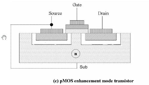
17 The n-channel depletion mode mosfet is different from n-channel enhancement mode MOSFET in having a channel by forming a thin n-type layer embedded underneath the gate. When a +ve voltage applied at the drain, a current flows through this channel even if the voltage at gate is 0 volts. As the gate voltage becomes more +ve, the channel becomes denser carrying a greater current (or) as the gate voltage becomes more negative, the channel becomes thinner carrying a smaller current. If the gate voltage decreases beyond threshold voltage, no current flows. The drain (o/p) characteristics from n-channel MOS, which may be, used either the enhancement or depletion mode. P-Channel Enhancement Mode: In this MOSFET with n-type substrate and with p + source and drain regions, on the other hand, the channel is p-type and device is called PMOS.
18 Symbols When voltages are applied to the drain, source and gate of p- channel enhancement MOS as shown in fig
19 A thin layer of channel for holes is formed underneath the gate and current, which consist of holes moving from source to drain flows. When the voltage of the gate becomes more -ve, the channel becomes denser and greater current flows. The channel has a thickness of less than 100 Å (in contrast, the insulation Layer between gate and substrate has thickness of the order of 100 Å ).The stream of holes is restricted to a very thin layer close to the surface, unlike the bipolar transistor where the stream of holes and electrons flows in a much deeper place. When the voltage at the gate increases toward a +ve voltage, the channel gets thinner and beyond a certain value, which is called threshold voltage, the channel is not completely formed and no current flows. [V GS > V T => I d =0] Comparison of P-MOS and N-MOS :- N-channel MOS have some inherent performance advantages over PMOS. The mobility of electrons, which are carriers in the case of an NMOS, is about 2.5 times greater than that of holes, which are carriers in PMOS.Thus n-channel is faster than p-mos. PMOS well suited technology and is less expensive than NMOS. PMOS enhancement is very popular in MOS systems because it is much easier to produce than n-mos. PMOS device must have more than twice the area of the NMOS device to achieve the same resistance.the NMOS can be smaller for the same complexity than PMOS devices. The higher packing density of NMOS also makes it faster in switching applications due to smaller junction areas. For all the above reasons it is clear that NMOS circuits are more desirable than PMOS circuits. However, the more extensive process control needed for n-channel fabrication makes them expensive and unable to compete economically with PMOS. conductivity factor k is high for NMOS and k is low for PMOS Threshold voltage (V T ) is high for NMOS and V T is low for PMOS. Turn-on time (t on ) is less for NMOS and high for PMOS.
20 1.2)operation of MOS,PMOS,NMOS transistors
21
22
23
24 1.3)Fabrication of CMOS inverter Basic CMOS Technology In early days of technology, the control gate of the MOS transistor was made with aluminum instead of polycrystalline silicon. It was difficult to align the metal over the channel precisely; an offset in one direction or other would create a non-functioning of the transistor. To overcome these problems, the poly-silicon gate was introduced. This polysilicon would be deposited before source/drain diffusion. During the diffusion, source and drain regions are self-aligned with respect to the gate. This self-alignment structure reduces the device size. In addition, it eliminates the large overlap capacitance between gate and drain, while maintaining a continuous inversion layer between source and drain. In the case of metal gate process, Al deposition has to be carried out almost at the end of fabrication because further high temperature processing would melt Al. In case of selfaligned poly silicon gate technology, these restrictions are also circumvented. Basic n-well CMOS process In a standard n-well process, one of the first things made is the n-well in a p type substrate. Once the n-well is created, the active areas can be defined. The MOSFET is build within this active area. A very thin layer of silicon dioxide is grown on the surface. This will be used to insulate the gate from the surface. The thin layer of SiO 2 is grown and covered with Si 3 N 4. This will act as a mask during the subsequent channel stop implant and field oxide growth. The channel stop implant is to prevent conduction between unrelated transistor source/drains. A thick additional layer oxide grows in both directions vertically where Si 3 N 4 is absent. Layer of silicon dioxide under the polysilicon gate (which will be created later) is known as gate oxide and that is not directly under the gate of a transistor is known as field oxide. The field oxide provides isolation between transistors. A threshold adjustment implant would be the next process step. This is carried out to balance off the threshold voltage differences. The P-MOS results in a higher threshold voltage level than nmos with normal doping concentrations. With additional negative charges buried inside the channel, V T for pmos could be controlled.
25 (a) (b) Formation of n-well Gate oxide covered with silicon nitride in the active areas Polysilicon deposition is carried out and gate definition is then completed using the mask shown in fig (c). Note that the connection between two gate inputs in a CMOS inverter is achieved using the poly silicon. The source and drain diffusions for pmos is carried out using p-type diffusion. Boron is the most popular element used for this step. Similarly, source and drain diffusions for nmos is carried out using n-type diffusion. Phosphorous and Arsenic can both be used for this step. Additional oxide is created, and then the contact holes are cut in the oxide down to the diffusions and polysilicon. These contacts can be filled by metal permitted to flow into the holes. The drains of pmos and nmos transistors are connected by a metal line in order to take the output from the CMOS inverter.
 Poly silicon gate definition")

26 Top view of Poly silicon mask (d) Poly silicon gate definition is completed (e) Transistor source/drain diffusion is completed (f)


27 P-well process Cross section of a CMOS inverter in an n-well process Prior to the n-well process p-well process was popular. P-well process is preferred in circumstances where balanced characteristics of the nmos and pmos are needed. It has been observed that the transistors in the native substrate tend to have better characteristics than that was made in a well. Because p devices inherently have lower gain than devices, n well process amplifies this difference while a p-well process moderates the difference. The standard p-well process steps are is similar to n-well process, except that a p-well is implanted instead of an n-well as a first step. Once the p-well is created, the active areas and subsequently poly gates can be defined. Later diffusions can be carried out to create source and drain regions. Finally, metal is deposited and patterned for contacts. Twin-Tub process It is also possible to create both a p-well and an n-well for the n-mosfet's and p- MOSFET respectively in the twin well or twin tub technology. Such a choice means that the process is independent of the dopant type of the starting substrate (provided it is only lightly doped). A simplified sketch of twin-well CMOS process cross section
28 MOS inverters: MOS inverters all use an enhancement-mode device (EMD) as a switching transistor to pull the O/P, because it can be switched off when I/P signal to its gate is low. In the off mode it draws negligible current from supply. The pull up can be simple resistor, an EMD operating as a current source with its gate connected to the positive supply, a depletion-mode device (DMD) operating as current source with its gate short circuited to its source, or a PMOS EMD acting as a pull-up switch. Switching circuit as discussed below: 1). The Passive Load NMOS Inverter: The simple NMOS inverter consists of an inverting FET and a pull-up resistor, as shown in figure. 1.v in <V T the transistor is in off, v out is pulled up to +ve supply voltage. In this case o/p is complement of i/p. 2.V in >V T the transistor is on and current flows from the v DD supply through resistor r to g nd. If R were sufficiently large, v out could be pulled down well below V T, thus complementing the i/p. Depletion mode is used as pull-up is formed by connecting gate of upper transistor to source.
29 The major problem with this inverter is the physically large pull-up resistor required. For a typical process, the on resistance of the FET (The resistance from the source to drain of the FET when gate voltage is high) might be in the order of 10 KΩ and sheet resistance (resistance of a square area) of the diffusion layer might be about 20 Ω/sq. The load or pull-up resistance must be larger than the on resistance or pull-down resistance of the FET in order for the O/P to go low when the pull-down transistor is conducting. If the pull-up resistor is to be at less than ten times larger than on resistance of the pull-down FET, then the value of the load resistance must be 100 KΩ, which requires a diffused pull-up resistor of 5000 squres length. This is unacceptably large. The width of the pull-down transistor can be increased to give an aspect ratio (L/W of the gate) of L/W=0.1 for the gate of the pull-down. This device requires a pull-up resistor 500 squares in size, but overall gate area is still unacceptably large.
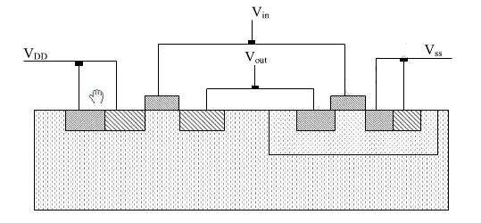
30 2). The Active Load NMOS inverter: a). PMOS Inverter: A much smaller inverter can be designed with a FET used as active load. The load can be enhancement-mode device or depletion- mode device. An enhancement-mode FET has no channel with zero gate-to-source voltage, and must have either a separate gate bias voltage or have its gate connected to its drain in order to be used as an active load. Depletion-mode device has a conducting channel with zero gate bias, and will not turn off until sufficient reverse bias is applied to its gate. To be used as a load device, the gate is connected to the source. The earliest MOS inverters consisted of p-channel FETs (PMOS devices) with aluminum metal gates and used an enhancement-mode pull-up configuration with negative logic, as shown in figure. Once feasible NMOS devices became available, they quickly replaced PMOS devices. Depletion-mode pull-ups have replaced enhancement-mode pull-ups due to their superior switching speed, as well as fact that the threshold voltage drop from gate to source required for enhancement-mode devices can only pull the O/P up to within a threshold voltage of positive rail. Enhancement-mode devices can be made to pull up to the positive rail, but this requires a separate gate bias which is greater than VDD by at least one threshold voltage. The major disadvantage of an NMOS load device is the fact that it never turns off and the inverter dissipates power whenever the pull-down device is on, just as passive resistance inverter does. This is one of the major concerns for popularity of CMOS design when power dissipation is a major concern. b). NMOS inverter:

31 The first type of active load investigated was enhancement-mode pull-up in figure, with the gate tied to the positive rail to keep the device on until the O/P voltage reaches threshold voltage below positive supply, at which point the pull-up switches off. NMOS inverters today usually depletion-mode loads devices as shown in above figure due to their better speed and pull-up characteristics. This will taken as the standard NMOS inverter, and NAND and NOR gates will be designed based upon this inverter. The depletion-mode inverter requires a separate ion-implant step to change the threshold voltage of the pull-up FET from enhancement to depletion type. This implant step is shown by a box around the pull-up device in the Stick drawing and by dotted lines to outline the implant area on the layout drawing.
32 The output from between the source of pull-up and drain of pulldown. The pull-up depletion transistor and it is usually to achieve proper inverter logic threshold. The relative locations of the saturation regions of pull-up and pull-down differ in their characteristics, due to difference in the threshold voltage of transistor. 1. While the input voltage is below the V T of pull-down transistor, no current flows in that transistor, o/p voltage is constant V DD drain to source voltage across pull-up transistor is equal to zero. 2. V in increased above enhancement mode Threshold, current begins to flow in the pull-down transistor. The output voltage decreases slowly as i/p voltage is first increased above V T subsequent increase in i/p voltage, until the point reached where pull-down leaves its saturation region. V INV -> The i/p voltage at which V in = V out is known as logic threshold voltage. The resistive impedance of MOS transistor is proportional to length to-width ratio of its gate region. Z Pu = (L pu /W pu )is increase relative to Z pd =(L pd / W pd ) then V inv decreases.
33 Down going transistor approximately f times the transit time of pull-down transistor. Up-going transistor approximately k times fan-out time s factor of pull-down transistor. To reduce R, W width should increase maximum. This is required diffusion process will increase. So the value of W is minimum and fixed, so we can make W increase gradually in number of stages i.e cascading of inverters. Transfer characteristics of n-mos inverter: To obtain inverter transfer characteristics we superimpose V gs =0 depletion mode characteristic curve on the family of curves for the enhancement mode device.
34
35 Q).Give the outline schematic for manufacture of VLSI ICs and explain it? Answer: Preparation silicon Wafer: Silicon material, diffusion, oxidation: Silicon semiconductor devices are fabricated on thin, single-crystal substrates called Wafers. These wafers are sliced from a cylindrical ingot of silicon and lapped and polished before processing. Depending upon crystal size, wafers vary in diameter from less than one inch to several inches. Electrical characteristics of the wafer substrate are determined by the doping type and concentration, which are contributed during crystal growing process. Electrical junctions are formed in the substrate by introducing the opposite type of dopant to a concentration that exceeds the bilk doping by means of solid state diffusion. Junctions can be obtained in selected regions by masking those areas of the silicon surface that are not be doped with a suitable thick layer of silicon dioxide. The oxide layer is grown by exposing the wafer to an oxidizing ambient of oxygen or water vapor, or both, at an elevated temperature in the range C to C. This is done in opened-ended cylindrical quartz tubes that are resistance-heated in special diffusion furnaces. This furnace provides precise control of temperature over a considerable length of the tube called flat
36 zone. Oxidation conditions are maintained so that an excess of oxidizing reactants exist in the tube atmosphere. This is done by introducing the reactants at one end of the furnace tube and allowing free exhaustion at the other end. Under this condition, temperature remains the controlling factor in oxidation, making it possible to grow a uniform oxide layer on many wafers within the furnace zone. Once oxide is suitably patterned by diffusion. Diffusion of dopants is usually accomplished by a two-step process. The first, called predeposition is used to introduce dopant impurities to only a shallow depth in the silicon. The furnace atmosphere is now comprised of a gaseous compound of the dopant atom, which coats the wafer surface. The compound in turn reacts with the silicon to form a dopant-rich surface layer, which serves as a source of dopant for further diffusion in the second step. This step is called drive-in diffusion, diffuses the dopant impurities into the silicon to the desired concentration profile. Diffusion is generally done in an inert gas atmosphere, but an oxidation step usually follows to form a productive layer over the diffused regions. Mask and etching: 1)In order to use silicon dioxide as a selective diffusion barrier, it is necessary to define the oxide coverage on the silicon material. This is accomplished by so-called photolithographic or masking process. The process patterns the oxide in a sequence that employs three key materials, a photographic mask a photosensitive material called photoresist and a silicon dioxide etching acid. The pattern on the mask is imaged on the photoresist film which, in turn, protects specific areas of the oxidized water from attack, when it is exposed to an oxide enchant. 2) Masks are photographically produced plates that have opaque device size patterns repeated on them. In this two steps are used. In first step the reduction image is repated for second reduction, to produce repeating the pattern in matrix fashion is called step and repeat. The positioning of repeated patterns must be done to exacting tolerances, since alignment of successive device levels depends on exact pattern positioning across the entire mask. The second step reduction pattern is then contact-printed to form the final masks or working plates. The working plates can be comprised of any of several materials, the most common being emulsion on glass. More durable opaque thin films, such as chrome metal, are also extensively used. The masks can be produced to have opaque patterns on a clear background or vice versa, depending on the material to be removed in subsequent etching and the type of photoresist used. 3). Photo resist, the second material, is an enchant resistant polymer is photosensitive when applied in this layers. The resist of negative type, it will be soluble certain liquid developers unless polymerized by exposure to intense light. Bu means of contact printing with the appropriate mask, the polymerization will notb occur under the opaque mask areas. The photoresist and suitable mask can
37 thus be used to obtain a device-pattern, etch-resistant film which is used, in turn, for selective etching of the silicon dioxide film. 4). The material used to etch the oxide is a solution of Hydrofluoric acid (HF). Usually, it is used in a buffered form containing ammonium fluoride to ensure more constant etching characteristics. When the photoresist patterned wafer is exposed to this solution, the oxide will be attacked in areas not covered by resist. For diffusion masking, the oxide is entirely removed from the regions by an enchant. Oxide enchant may be required for extra diffusions, contact openings, or thinning oxide regions. These remasking steps must be performed so that subsequent layers are accurately located with respect to preceding ones. This registration is ensured by a technique called mask alignment with mask aligner. 5). Masking techniques are also employed when diffusion regions are to be connected to form circuits. The interconnection medium used is a metal film or combination of films. After etching contact openings through the oxide down to the diffused regions, the wafer is coated with a thin metal film, usually by evaporation. The metal to be deposited is heated in a vacuum system until vaporizes, uniformly coating the wafer surface. Aluminum is the metal used most often. The metal film is then defined into the desired pattern by the same photoresist methods as by selecting a suitable metal enchant. Assembly: 1)The separation of individual circuits from the wafer substrate is the most commonly done by a procedure called scribing and breaking. This is accomplished by taking advantage of the natural tendency of the silicon wafer to cleave along certain crystal planes. During the ingot sawing operation, the wafer was asymmetry, or flat, to index the orientation into account. When the completed wafer is oriented and scored with a diamond scribe, including localized crystallographic stress, it is broken along the lines into the separate fragments called dice. 2).The next step is dice encapsulation. Besides being a productive enclosure for the device, a package must also provide a means for connecting the contact points on the die to the external leads. The dice are mounted on package substrate, usually means of thermal solder type attachment. This die attach step, in addition to mechanically securing the die in this package, provides an electrically conductive connection to the silicon substrate. This also allows the heat generated in the circuit to be dissipated by conduction into the package. 3). Connection to the contact points or pads on the die is then accomplished by wire bonding. In this lead binding operation, one end of a fine metal wire typically 1 mil in diameter is attached to the die pads and the other end is
38 attached to the package bonding lands. The package is tube heated in such a manner that the lands in turn are connected to the external package leads. Lead bonding is separated for each pad to be connected. Other method are automated methods by which all contact points are made simultaneously developed, but these require speed of wafer preparation or highly specialized packages 4). The last assembly operation is to finalize the encapsulation by isolating the sensitive circuit from its environment. By attaching over the package substrate while it is in an inert gas ambient, the die is hermetically sealed. Direct encapsulation of the die in plastic materials is also possible for certain circuits require special wafer preparation. Metallization: It is process by which the components of ICs are connected together by Al conductors. The fabrication process forms on the wafer that creates wires and transistors. Wafer contains many circuits fabricated as Batch process. This process is efficient because we can produce many identical chips by processing a single Wafer. By changing the masks that determine what patterns are laid on the chip, to make particular circuit on the chip. To build it on an IC fabrication line, we must go one step further and design the Layout, or patterns on the masks. The rectangular shapes in the layout (stick s diagrams and layout diagrams) for transistors and wire which confirms the circuit in the schematic. Creating layouts is very time-consuming and very important- the size of the layout determines the cost of manufacture the circuit, and shapes of the elements in layout determine the speed of the circuit as well. Photolithography: The purpose of this is to open windows whenever diffusion is to be done and retaining Sio 2 remaining areas. During manufacturing, this step (photographic printing) process is used to transfer the layout patterns from the masks to the Wafer. The pattern left by the mask are used to selectively change the wafer: Impurities are added at selected locations in the wafer, done by diffusion and insulating materials by Oxidation (Sio 2 ), the conducting materials are added at the top of the wafer as well ( Metallization). Oxidation: It is a process where by oxygen molecules from a gas above the substrate or surface material cause the growth of the oxide on the surface. Since substrate or surface is silicon material, the oxidation process produces Sio 2. The aped at which silicon dioxide layer grows is a function of doping concentration and temperature of substrate during oxidation. It serves as a very high good insulator between substrate or surface material. These fabrication steps require very high temperature (> C), small amounts of toxic chemicals, and extremely clean environment. Diffusion: It is process for fabricating technology dependent transistor. In this impurity atoms moves from high concentration region to low concentration
39 region to get desire width of source and drain of MOS transistor. From mask information the gate terminal laid on silicon substrate by using polysilicon material. Separation of ICs: This is done by Dicing Saw method. In this method the individual chip is separated from Wafer. Because the no manufacturing process is perfect, some chips on the wafer may not work. Since at least one defect is almost sure to occur on each Wafer, Wafers are cut into smaller, working chips, the largest chip that can be reasonably manufactured today is over 1,5 cm on a side, while Wafer is in the 20-25cm. Each chip is individually tested; the ones that pass the test are saved after the wafer is diced into chips. The working chips are placed in the packages familiar to digital designers. In some packages, tiny wire of Gold wires connect the chip to the package s pins while the package body protect the chip from handling and the elements, in others, solder bumps directly connect the chip to the package. Package and Tests: To give strength to IC and protection from environment packages are required. Testing is a process of verification to make process parameters within the tolerances acceptable for the product. Pads: The dimensions for metal bonding pads have not scaled with decrease in feature size of the process. The size of capillaries used for attaching bonding wires, which are several mils in diameter for bonding actual circuit on silicon wafer to IC pin pads. IC technology manufacturing is a powerful technology for two reasons: All circuits can be made out of a few types of transistors and wires, and any combination of wires and transistors can be built on a single fabrication line just by changing the masks that determine the pattern of the components on the chip, ICs run very fast because the circuits are very small Silicon wafer preparation: 1). Oxidizing. 2). Removing organic residues. 3). Backside crystalline damage. Characteristics of Substrate: 1). Surface crystalline orientation: It has a major impact on the electrical device characteristics (reflected in carrier mobility & Q ox terms) & also strongly influences process development. The introduction of impurities into crystal by ion implantation relies on collision with atoms at lattice sites to slow the impaging ion. The surface orientation also strongly affects the thermal oxide growth. 2). Wafer diameter, Wafer thickness & surface flatness: The mechanical & chemical polishing of active device surface after wafer sawing will enhance the wafer flatness, nevertheless, the tolerance on this specification
40 will affect the ability to keep 1:1 mask image in focus when exposing a photo resist coated wafer, which makes a tight flatness specification more difficult to achieve. The defocusing of the image of a large field at wafer surface is aggravated by the presence of a dielectric film holding the surface in tension or compression, as a result, the wafer will warp. The wafer thickness must be increased at large diameters to reduce this effect. Silicon occurs in naturally in the form of sand. Chemically it is known as Sio2. Silicon accounts about 26% of earth crust. The stages of process of wafer preparation are: 1). Chemical reduction:by chemical process, sand is treated, to produce impure silicon. This is to be further purified to a better degree, typically of the order of 1 part in 10 6 i.e. impurity atom for silicon atoms. This is achieved by Zone refining. 2).Zone refining: The impure silicon, obtained from reduction process, in the form of rod, is heated to produce a small molten zone. Impurities in the zone tend to float to the zone boundaries. If the molten region is slowly moved from one end of the rod to the other the impurities collect at the ends (due to temperature along the length of the rod) and so impurities can be removed. In thermal process temperature is about C. This process is repeated several times to get the required degree of purity. The degree of purity will be tested by knowing the conductivity σ of silicon rod. For device applications, the silicon must flaw-free as possible. i.e it must have a regular structure. Such a single crystal structure is obtained by crystalline pulling is known as CZOCHRALSKI process.
41 3). Crystall pulling CZOCHRALSKI process:
42 Previously produced single crystal silicon is used as seed crystal. This is touched as the surface of the melt then slowly rotated & with drawn. Now if controlled amount of impurities are added to the melt, p-type or n-type silicon can be obtained. Speed of with draw: 50mm/hr. The ignot obtained is sliced into wafers of 0.3mm to 0.5 mm thick, using a diamond impregnated cutting edge. The wafers are ground & lapped. One face of each wafer is polished to a mirror finish & inspected under microscopic because, the surface must be smooth & on this side Sio2 is grown so that the thickness is uniform. Wafer diameter: 75mm or 100 mm. Wafer thickness: 0.1 to 0.25mm. OXIDATION The growth of thermal oxide from silicon substrate is the fundamental process step of MOS device fabrication, a reproducible, low resulting defect density, contamination-free process technology for gate dielectric for the device & surface to interconnection dielectric layer. This is an essential step in the planar-diffused process of silicon technology. Oxide layers are used as elements in active & passive devices on silicon functional process. Function of oxide layers: 1).It protect silicon surface from undesirable atoms. 2). As a dielectric. 3). For dielectric Isolation (for ICs). 4). Impurity masking during diffusion. Oxidation Kinetics: The chemical reaction associated with oxide growth involve either an oxygen(dry) or water vapor(wet) ambient. Si + O 2 - Sio 2 -- (1) and Si + 2H 2 o Sio H 2. The evaluation of Hydrogen from 2 nd reaction through the oxide layer out of the ambient will result in some reactivity with oxygen atoms is gone, resulting in a more porous film. The dry oxidation process uses high-purity oxygen(o 2 N 2 mixture). The wet oxidation introduces water vapor into the furnace tube. The ratio of silicon consumed from the substrate to the resulting oxide film thickness is The thermal oxidation of silicon results from diffusion of oxidizing species through
43 the existing oxide layer to react at the substrate surface, in a steady-state condition, the following flux densities must be equal. 1). The transport of the reactant from bulk gaseous ambient to oxide surface. 2). The diffusion of the species through existing oxide layer. 3). The reaction-rate at the oxide-silicon surface. Types Of Oxides: 1). Thermal Oxides: Such oxides are formed by thermally activated reaction of silicon with oxygen or wafer. 2). Anoidic oxides: these are formed by anodization. In a liquid medium, electrodes are placed & charged ions move. Negative ions towards positive electrode & positive ions towards negative electrode. Then oxide layers will be formed on the silicon wafer. This is similar to electrolysis process. 3). Deposited oxides: Oxide layer is deposited on the silicon wafer by vacuum deposition process. Silicon wafer placed in a vacuum chamber is deposited with oxide layer. It costly process. Thermal oxidation method is commonly used. Again there are divided into 3 types. 1). Wet Oxidation:
44 Dry oxygen is passed along with steam (from boiled & distilled deionized water) over wafers. Diffusion coefficient lies between the dry and steam methods. Dry oxides are more sensitive to cleaning treatment. Steam oxides difficult to combolt. So wet oxidation method gives best results. Different colors can be get after oxidation : Bluish Green, Yellowish, Violet etc. 2). Dry oxidation: dry oxygen is passed over wafer in a furnace. Si+ O 2 Sio 2. Growth rate of oxidation is evaluated by a term known as diffusion coefficient D. D(O 2 ) at C = 2.82X10⁻¹⁴ cm 2 /sec. Thickness of oxide layer is 5-10 µm simple applications.
45 3). Steam oxidation: Oxide layer is deposited on the silicon-wafer by steam is passed over silicon wafer. Diffusion coefficient D is D(H 2 O) at C = 9.5X10⁻¹⁰ cm 2 /sec. Si + 2H 2 o Sio H 2. Growth rate of steam oxidation process is high. Q).Explain the properties of the thin oxide (Sio 2 )? Answer: OXIDE PROPERTIES: 1). The index of refraction of dry oxides decreases with increasing temperature, the apparent density of oxides grown at 8000C is 3% more than those grown above 11900C. The etch rate of thermal oxides at 1000A0/min but varies with temperature and etch solution. The etch rate also varies with oxide density and thus with oxidation temperature. Measurement shows that high-pressure oxides grown at 7250C and 20 atm exhibit a higher index of refraction, higher density. For thin oxides, the role of the interface in determining oxide properties is important. 2). Masking properties: A silicon dioxide layer can provide a selective mask against the diffusion of dopant atoms at elevated temperature, a very useful property in IC processing. A predeposition of dopant by ion implantation, chemical diffusion are important at or near the surface of the oxide. During hightemperature drive-in step, diffusion in the oxide must be slow enough with respect to diffusion in the silicon that dopants do not diffuse through the oxide in the masked region and reach silicon surface. The values of diffusion constants for various dopants in Sio 2 depend on the concentration, properties and structure of Sio 2. A commonly used n-type impurities P, Sb and As, as well as the most frequently used p-type impurity B, all have very small diffusion coefficients in oxides and are compatible with oxide masking. Dopants Diffusion Constants at 11000C (cm2/sec) B 3.4 X to 2.0 X Ga 5.3 X P 2.9 X to 2.0 X As 1.2 X to 3,5 X Sb 9.9 X Oxide grown in dry oxygen have best electrical properties but sometimes wet oxidation is preferred. Like when thin oxides are required in MOSFETs for fabricating gate oxides then dry oxidation is preferred for fabricating thicker oxide regions like field oxide, wet oxidation is used.
46 Thin Oxides: In sub-micron range MOS VLSI very thin oxide (50 to 200 A 0 )) are grown on crystalline silicon. These oxides show good electrical characteristics and provide long term reliability. Oxides also serve as dielectrical material for MOS devices. The growth of thin oxides must be slow to obtain uniformity and reproducibility. A number of growth techniques are there like dry oxidation, wet oxidation, reduced pressure techniques and high pressure/low temperature OXIDATION. Ultra thin oxides and thickness less than 50 A 0 can be grown by using nitric acids, boiling water and air at room temperature. Rapid thermal oxidation performed in controlled oxygen ambient with heating provided by tungsten-halogen lamps is also used to grow thin oxides. Properties of Thin Oxides: 1). At reduced temperature oxide density increases. 2). Index of refraction of dry oxides decreases with increasing temperature. 3). Density of oxides grown at low temperatures is more than that grown at higher temperature. 4). Etch rates of Thermal oxides varies with oxide density and with oxidation temperature. 5). Higher pressure oxides exhibit higher index of refraction, higher density and slower etch rates in buffered HF than steam oxide. 6). Silicon dioxide layer provides a selective mask against the diffusion of dopant at elevated temperature. Q).With neat sketches explain the electron lithography process?
47 PHOTOLITHOGRAPHY The purpose of this is tom open windows whenever diffusion is to be done & reaction Sio 2 remaining areas. In the fabrication process this step is done after oxidation. Photolithography is also done before metallisation, whenever metal contacts are to build up. This process is carried out in a clean room where UV light is not present. Yellow color light of a particular wavelength are employed so that, light in UV range is not present, since UV light effect the photo resists. The operation is carried out in a clean bench, where, dust free; pre clean air is blown continuously. The different steps in photolithography are: 1). Wafer cleaning. 2). Mask preparation. 3). Photo resist coating. 4). Exposure to UV light. 5). Developing. 6). Etching. 7). Removal of photo resist & cleaning. NEGATIVE PHOTORESIST: (a mixture of resin & photosensitizer) Crosslinks upon absorption of UV radiation, the resulting high-molecular weight polymer chains are insoluble in negative photo resist developer solvent solution. Transparent areas of mask correspond to areas on wafer where the protective photo resist coat of negative photo resist remains. Disadvantages: 1). The necessary cross-linking of long polymer chains to inhibit dissolution by developer limits the fundamental resolution of negative resists. 2). The negative photo resist developer is largely composed of a solvent to remove the low-molecular weight, non cross-linked polymer resin, this solvent is absorbed to some degree by exposed negative resist, which swells the remaining resist film. Positive resist developer is a solution, which doesn t result in image swelling. 3). In stop-repeat aligners, a high-intensity, short duration exposure is necessary to maintain high effective throughput. The reciprocity of a photosensitive medium is extent to which intensity X time product necessary for exposure (given thickness) remains constant over range of intensity indeed reciprocal, while negative resist are not ohms, the determination of proper exposure time (using light integrator) is difficult for negative resists. 4). Negative resists are also more sensitive to low levels of exposure energy than positive resists, in othetrwords, the negative resist have less contrast. The reflectivity & scattering of incident light from the wafer film below (an aluminum metalliztion layer) tends to cross-link resist in areas outside the original image. Source of photo resist are: 1) KODAK (Kodak photo resist). 2). KMER: Kodak metal etch resistor. 3). KTFR: Kodak thin film resistor. 4). VISTAK: Indian telephony industries. 5). AGFA: Positive, negative.
48 6). Dynmo-chem. Photoresist coating types: 1). Dip coating. 2). Spry coating. 3). Spin coating practically it is used & it gives uniform coating. 4). Flow Coating. Photolithography Steps: 1) Apply resist Adhesion promoter to wafer: For most surface film that is to be coated with resist (SiO 2, Si3N4, Polysilicon)& Adhesion promoter is initially applied. Adhesion promoter (hex methyl disilazane (HMDS)) is applied to wafer surface by spin-coating technique using high rpm, high-acceleration-rate wafer chuck, the wafer is held by vacuum. 2) Application of resist: Again using a spin-coat wafer chuck system, a precise amount of resist is dispensed onto wafer surface, allowed to dwell momentarily & then spun at high rpm to throw excess resist off the wafer into a collecting bowling-shape shroud. The chuck spin speed, spin time & acceleration rate selected to produce a particular resist film thickness & uniformity. The resist is filtered during application to remove particular contamination. 3) Resist exposure: After alignment, the photo resist coat is exposed to UV through the transparent and opaque mask areas. The selection of proper exposure time and focus is typically made from inspection of the resulting patterned image, on a step-and-repeat reduction aligner, a focus-andexposure matrix is commonly produced initially on a non-product wafer and the optimum developed image is selected after inspection to determine exposure characteristics often measure of a reference photo resist line width in the mask kerfs made to assist in selecting optimum conditions. 4) Resist develop: The exposed resist film is then subjected to a developer solution to produce the latent resist pattern. The dissolution ratio between exposed and unexposed areas in commonly large (positive photo resist), but the developed time and temperature must nevertheless be controlled quiet accurately. The quenching of the developer action by a subsequent rinse follows immediately. Batch impression developer bath with agitation. The rinse follows immediately after develop time expires while the wafer continues to spin.
49 5) Resist post bake (After SiO2 etching): The final resist treatment step (prior to etching of exposed film) is post bake at elevated temperature (30mm bake at C in oven). This step increases the etch resistance of the coating, enhances the resist adhesion to the underlying layer, and drives off remaining solvents. Careful consideration must be given to the temperature and time of post baking so that the plastic flow of resist film doesn t severely alters the developing image, in some cases, a slight reflow of the resist may be used for the side wall profile to control in the resulting etched film, if the resist and film are removed at comfortable etch rates. This sequence of steps describes the conventional photo resist processing techniques. Alternative steps are taken to produce resist sidewall profiles with a slope suitable for metallization lift-off procedures. 6) Removal of photo resist: The complete removal of photo resist coat after etching is a key process step to eliminate contamination in subsequent processing. Resist removal is complicated by exposure to a high temperature ion implantation or plasma etch procedure.
50 Q).Explain the photolithography process? What are recent developments in lithography Advanced photolithography: Electron beam X-ray lithography Photo exposure full wafer Resolution(R)µm Through o/p (N) Wafers/Hr System cost (C) K$ Clean room area (A) Sq.Ft. Figure of merit N(10 3) / (C+10A)+R
51 1).Electron beam Lithography: The resolution in electron Lithography is much higher than photolithography due to small wavelength (less than 1 angstrom) of the KeV electrons. In such case the resolution is not limited by diffraction, but by electron scattering in target materials including the resist by various operations of electron. This method is widely used for pattern generating functions. Some of these applications are mask-fabrication for photo or X-ray lithography, direct reaction with some materials on the wafer and direct writing on the wafer. It is classified into two types: 1). Scanning. 2). Projection type. The scanning type is divided into two categories i.e. Restore and vector scanning. Figure shows the exposure sceme. In this CAD system, the VLSI pattern is made. The O/P format from CAD systems is converted into the internal format of individual exposure systems. The data is decomposed into simple elements (trapezoids or rectangles depending on machines) by electron exposure machines. Since, the electron beam exposure machines handles data function also, it is bigger than the optical printers. Some special products such as microwave transistors. The direct writing has been applied in some low-volume production devices. These direct writing M/Cs are also applied in development stages of VLSI and in personalization pf ASICs to minimize the mask related cost, and development time. 2). X-ray Lithography: In this the diffraction effects and resolutions are improved by reducing the wave length. If wave length is reduced further than deep UV, all optical materials turns to opaque due to fundamental absorption. But transmission increases again in the X-ray region. The development of this type in In this Lithography, X-ray source illuminates a mask which casts shadow on a resist coated wafer. The main components of this type process are 1). A mask comprised of a device pattern made of X-ray absorbing materials, 2). An X-ray resist and 3). X-ray source. Figure shows the several materials for X-ray absorption. The absorption coefficient of an element material of density ρ and atomic number Z is proportional to ρz4 λ3 over wide range of wave lengths. In this type, the resolution and placement accuracy obtained so far is 0.2 µm and 0.3µm respectively. Epitaxy Epitaxy is Greek word. Epi means ON taxi means Growth. Growth of Si atoms or crystals on the surface of Si itself is called epitaxial growth. Epitaxial Si layer grown onto the starting crystalline substrate material. Bipolar device IC technologies have long been developed dependent on the epitaxial layer during device fabrication. In CMOS that
52 an epitaxial layer be present on the substrate prior to beginning of fabrication. The impurity concentration in the epi layer is relatively independent of the background concentration of the wafer substrate. The epi layer can therefore be a high resistive layer with a low resistivity, bulk region below. The high resistivity epi layer is attractive for reducing junction capacitance and threshold voltage body effect coefficients. The low-resistivity substrate is selected to reduce the localized substrate resistance and substantially reduce the gain of one of the parasitic bipolar transistor type. Experimental Setup:
53 The deposition of an epitaxial layer can be performed in a cold-wall system with wafers lying horizontally on an inductively heated susceptor. In this Si atoms deposited on the wafer surface be sufficiently mobile so as to allow for incorporation into a crystalline lattice site. Epitaxial Si can be grown using any of the following reactions Silicon tetrachloride is used as the source and it is reduced to silicon at high temperature. SiCl 4 + 2H 2 Si + 4HCl C, µm/min. SiHCl 3 + H 2 Si + 3HCl C, µm/min. SiH 2 Cl 2 Si + 2HCl C, 0.4-3µm/min. SiH 4 Si + 2H C, µm/min. To get n-type silicon epitaxial wafer. Phosphine gas is used as impurity source. (For p-type bi borne is used). Epitaxy is carried to achieve: 1). Near perfect crystalline structure for the active regions of the device. The substrate acts as a path for carriers if the crystalline structure is not perfect, device characteristics will be effected (leakage etc.).the presence of flaws (crystal defects) leads to reduction of lifetime of the carriers. 2). Series resistance associated with the device can be reduced. Epitaxial process a single crystal silicon (silicon atom layer) from the gas phase is deposited on existing crystal wafer (silicon wafer). The epitaxial layer may be p-type or n type. By epitaxial growth, the series resistance associated with the substrate can be reduced without changing the characters of the semiconductor device. Advantages of Sicl 4 : 1). It is easy to purify. 2). It is non toxic & inexpensive. 3). The reaction making silicon from Sicl 4 takes place at surface and not on the boat or reaction changes walls. Disadvantages : 1). The growth process is accompanied by different phenomenon. 2). Sicl 4 requires higher temperature. By epitaxy, crystal is grown slowly, so near perfect crystalline structure will be obtained & the conductivity of grown layer can be controlled effectively. In czpchralski pulling method, crystal defects will be there & controlling conductivity difficult. Because of crystal defects, electrical properties will be affected.
54 Q).With help of a neat schematic describe the ION Implantation process? Why it is prefer for VLSI fabrication? What are advantages and disadvantages? Q). Compare thermal diffusion process with ION Implantation process? ION IMPLANTATION Ion implantation is a technique for introducing a precise quantity of impurities into the substrate by accelerating a beam of ionized impurity atoms in vacuum to impinge on the wafer surface. The impurities may be added to material in selective areas, where locally from reaching the substrate by photoresist coat or thermal oxide layer of sufficient thickness. In diffusion process the diffused portion of the IC through windows is not diffused exactly perpendicular to the surface of the substrate, instead it diffused laterally under Sio 2 layer (Horizontally) also shown in figure. But the length and width of these diffused areas accounts the characteristics of ICS. To avoid this we can use another technique to overcome this difficulty called ion implantation whose block diagram is shown below.
55 The ion source must be able to provide a relatively high current level of desired ion species( in 10µA to 1mA range) in order to reduce process time. The ionization coefficient describes the number of ionizing collisions produced by an electron passing through gas(per unit length per unit pressure). The resulting ions that penetrate the screen opposite the cathode are accelerated by electric field between the screen and extraction electrode. The beam column is evacuated to reduce ion gas molecules collisions, which could result in unwanted deflection or charge neutralization of the ion. The e/m ratio of the material is specific to the material. So when the ions traveling with e/m we can adjust electrically to travel only specific ions towards the target & they impurities can be eliminated. The magnetic field analyzer bents ion beam towards the target. The scanned plates the ion beam can be deflected. The characteristics of the devices are superior.
56 The beam current provides the number of ions per second incident upon the wafer. A major advantage of ion implantation is the accuracy to which this dosage can be controlled over range of to ions/cm 2. Specifications: Target temperature: 196 to C Pressure in beam chamber: 10-5 to 10-2 PASCAL s. Depth of ion implantation: 0.01µ to 5µ( Not possible with thermal diffusion). The ion beam current: 1 na to 20mA. The ion beam CSA : 0.1 to 1 cm 2 Disadvantages: Cost is High $500,000. Q).Clearly explain the diffusion process in IC fabrication? DIFFUSION Any fabrication process is the impurity profiles of all junction nodes, the targeted junction depth affects the design rules of device length & node-to-node spacing. While the surface concentration must be sufficient to provide ohmic contacts to metal to inter connect. The integral of the profile determines the electrical sheet resistivity; the shape of profile in the vicinity of junction depth determines the junction capacitance. Thermal diffusion is an important physical process in IC fabrication. In this process particles moves from region to high concentration to region of low concentration. Diffusion of impurity atoms on silicon crystal takes place at elevated temperature C. 1). Substitutional Diffusion : Here the silicon atoms of the present crystal will be displaced by impurity atoms because of its high thermal energy. Impurity may be donor or Acceptor. n-type Impurities are : Phosphorous, Arsenic & Antimony. p-type Impurities are : Boron, Aluminum & Iridium. 2). Interstial Diffusion: Here the impurity atoms doesn t replace the silicon atom, but occupies Vacant places or Voids in the lattice. Gold, Copper & Nickle are the impurities, which diffuse interstially into silicon atom. This type of diffusion depends on the nature of the Impurity atoms. It is low temperature process. Interstial diffusion is done to reduce carrier lifetime and increasing switching speed. For Digital ICs the method is employed. Diffusion process is governed by Fick s first law : F = D N/ x--- (1) Where N-- number of impurity particles per unit volume. x-- Distance measured from the surface into which diffusion takes place. D-- Diffusion coefficient m 2 / sec. F-- Particle flux density between two surfaces in semiconductor wafer.
57 Statement: The particle diffusion rate(from high concentration to low concentration, is proportional to the concentration gradient N/ x of impurity atoms. Negative sign is there because particle from & concentration gradient are in opposite direction(particles move from higher to lower concentration, so the gradient sign is opposite. Fick s second law: N/ t = D 2 N/ x 2 The rate of change of impurity concentration with respect to time is proportional to the second derivative of the concentration gradient with respect to coordinates. Value of D depends upon doping impurity temperature, time. N -- Based upon this we can control F. The impurity distribution takes place in two ways: 1). Constant source diffusion. 2). Limited source diffusion. 1). Constant source diffusion: 1). Suppose in the diffusion process, the silicon wafer is exposed to a volume of gas containing number of impurity atoms(say n- type impurity) per unit volume. 2). Let the distribution of these impurity atom is uniform through out the gas. 3). The impurity atoms will get diffused into wafer, along the thickness of the wafer due to high thermal energy possessed by impurity atoms, Assume that impurity atom concentration at the surface of the wafer is N0 & it remains constant throughout the diffusion process, then the distribution of impurity atom, along the thickness of the wafer surface will be as shown: N Concentration of impurity atom on the surface. t-- time, x--- distance along the thickness of the wafer. The curves are obtained by starting by solving differential equation N/ t = D 2 N/ x 2 with boundary conditions, that N 0 is constant through from t=0 to N(x)=0 at t=0 in the beginning (when diffusion is not started impurity concentration = 0). The solution of the differential equations is N(x,t)=N 0 [ 1- erfx/(2 Dt)] where erf - error function. Or N(x,t) = N0 erfc/(2 Dt) where erfc - complementary error function. Any error function Y erf Y = 2/ x e x 2 dx. erfc =1-erf y. So we get that type of curves. Because we are assuming that the concentration of impurity atoms N 0 is constant, it is constant current source diffusion.
58 2). Limited Source diffusion: Here diffusion takes place in two steps. 1). Predeposition : A fixed number of impurity atoms are deposited on silicon wafer during a short time. 2). Driven deposition: Now, the impurity source is removed and pre deposited impurity atoms will get diffused into the wafer. Here the boundary conditions are N(x) = 0 at t=0 for x>0 i.e. before diffusion, the impurity atoms will zero. Q = N(x) dx for all where Q is total number of impurity atoms per unit area. A fixed number of impurity atoms are deposited. N(x,t) = (Q / D t) e x 2 /4Dt. This is known as Gaussian distribution. The area under these curves will be the same since Q is fixed. Junction profiles will be different in both cases. Impurity in the form of Diffusion source.
59 Impurities type Donor (N) Acceptor(P) Solid P BN Liquid Pocl 3 Phosphorous oxide Gas P 2 o 5 phosphine Parameters affecting Diffusion process: 1). Diffusion Temperature: High temperature gives more & thus higher relocities to the diffused impurities. Diffusion coefficient D depends on temperature T.
60 2). Diffused time: As the diffusion time is more, more number of carriers will get diffused to a great depth, so junction depth depends on the time. 3). Surface cleanliness: The silicon surface & the diffusion furnace must be absolutely clean. Otherwise impurities of doping will be last & also the characteristics of the junction will be affected. 4). Solid solubility: it is the maximum value of N0(impurity ion concentration on the surface) which can be deposited(or dissolved) on silicon wafer. Problem on Diffusion : Metallization Generally Aluminum is used for metallization to interconnection it is done before encapsulation. It has properties: 1). Deposition rate and grain size control. 2). Adhesion to underlying dielectric films. 3). Temperature limitations is subsequent process steps after deposition interconnect. 4). Ductile nature of interconnect, susceptibility to micro cracking. 5). Diffusivity of metal into silicon. 6). Growth of metal oxide surface layer. 7). Susceptibility to corrosion & attack by water vapor. Properties:1). It is cheap. 2). High electrical Conductivity. 3). Thickness of Aluminum conductor 1500A 0. 4). Sheet resistance is ohm / Square. Process: It is process by which the components of IC are connected together by aluminum conductor. First the entire wafer is coated with aluminum. Then by using metallization masks, aluminum is removed from the portions where contacts are not to be taken or conducting region is not required aluminum is deposited by vacuum deposition technique. Vacuum deposition technique:
61 Here the substrate is commonly deposited by metal evaporation of a solid source in a high vacuum chamber with subsequent condensation on substrate targets. The yield of target atoms released for each incident ion, the deposition rate onto the wafer substrate is proportional to the incident ion density & sputtering yield. The sputtering rate also increases with temperature. The sputtering yield of the target material using ions generated in a gas discharge is reduced due to increased gas-ejected target atoms collisions at the operating gas pressure (5 to 40(10-3 )torr) with subsequent redeposit ion onto the target.
62 Encapsulation : There are different methods by which encapsulation can be done, for digital ICs conducting tools are used to conduct the pins of the base to the terminal points of IC unit. ISOLATION In monolithic IC all elements, transistors, diodes, resistors etc. are formed within a common conducting substrate. Often the substrate resistivity may not be high, so each element should isolate from the other. And the elements must be interconnected through metallization only & not through the conducting substrate, Hence isolation of elements one from the other is required. Different Isolation techniques are : 1). Diode Isolation: 1). Circuit elements are formed with in an epilayer which is grown on substrate of opposite type(n epilayer on p type substrate). Now isolation islands are formed by heavily doping the same type of impurities as the substrate. If the substrate is p-type P + diffusion is done through the epilayer till it meets the substrate. 2). To achieve this type oxidation is done, all over epilayer. 3). Using photolithography, windows are opened. Now P + diffusion is done to a depth equal to epilayer. 4). So n type separate islands will be formed. So the n type separate islands & P+ region will act as a diode. Each n islands is isolated from the other. The transistors, diodes etc. are made on each n island. They all interconnected by metallization as per the circuit. Thus elements are isolated one from the other within the substrate. The diodes are maintained at reverse bias by connecting the p-type substrate to most negative potential in the circuit via surface metallization. Advantage: Only diodes are to be fabricated so it is cheap. Disadvatages: 1). Isolated diffusion (P+ diffusion for p-substrate) is deep as thick as epilayer. So diffusion time is more.
63 2). Lateral diffusion will also takes place while vertical diffusion is taking place. So widthwise, clearance must be given on the wafer. So this will result in inefficient chip area. 3). The capacitance of larger area isolation diodes will affect the circuit performance at high frequency. 2). Dielectic Isolation: In this case each island, in which an element is deposited, is isolated from other by a dielectric (Sio2) layer. Thus Isolation is provided. This is carried out with the following steps: 1). The starting material is n type silicon wafer not n or p epilayer. It can also be p-type silicon wafer. 2). Oxidation: Oxide layer is grown all over. 3). Photolithography: Using a mask, windows are be opened where ever islands are to be created. 4).Silicon etching: When ever windows are opened etching of silicon is done to a depth of 10-15µ using buffered HF(Hydrogen Floride) solution.
.")
64 5). Reoxidation: Now, reoxidation is done so that the etched portion of silicon is also coated with oxide layer. 6). Then a silicon layer is grown all over to a height of µ. 7). Now wafer is inverted & bulk of the original n type region is etched &lapped away until only n-type island remain in the polycrystalline substrate. Advantages: 1). No frequency limitation & perfect isolation parasitic capacitance as in the case of diode isolation is less because oxide thickness is more. 2). Permitivity of Sio2 is 1/3 of that of Silicon. Disadvantages: 1). Number of process steps are more. 2). Lapping operation is difficult. 3). Silicon on Saphire (SOS) Isolation: Device fabrication use of crystalline sapphire Al 2 o 3 layer on insulating substrate. Sapphire is perfect insulator. This choice can effectively result in elimination of the area of device node junction capacitance. So isolation can be provided. 1). The deposition of silicon epitaxial layer into a crystalline material whose lattice parameters similar to that of desired surface orientation (ex. 100 silicon on ( ) sapphire (Al 2 o 3 ). 2). The deposition of polycrystalline onto a non-crystalline (amorphous) substrate, with subsequent recrystallization on the deposited film. Silicon is etched from islands, so that isolation is achieved. Advantage: The process is simple, isolation is perfect, No frequency limitation or capacitance problem.
65 Disadvantages: 1). Potential problem with this technology options are aluminum auto doping, thermal expansion coefficient mismatch & film defect density( i.e. a strong function of distance from the silicon-insulator interface). 2). Sapphire is costly, so it is used for high frequency ICs only. Cross Overs: In the electronic circuit i.e. to be incorporated in IC, there will be interconnections or crossovers. For interconnections one element cross over, two conducting patterns should be separated from one another. An example, consider the Multivibrator circuit, two transistors are connected as shown: So the metallization pattern conducting C1 to B2 & C2 to B1 shouldn t touch each other. So there must be a crossover. How to realize this? The method to be adopted should be compatible with IC technology. One method that employed is buried crossover. It is shown in figure:
66 Two elements A & B are to be connected by conducting pattern. There is another conducting pattern over crossing this. But it shouldn t start the previous conducting patterns. This can be realized shown n+ region in the buried conducting pattern. The elements A & B (they can be n-type emitters of the transistor) are connected through n+ region. Heavy diffusion of n+ is done along with the emitter diffusion. So A & B are interconnected through n+ region. Sio2 separates the other conducting pattern of aluminum from n+ conducting pattern. The crossover is achieved. Another method is to have a diffused resistor in between the two conducting patterns to separate them, to get crossovers. A diffused resistor is lightly doped semiconductor material with high resistivity. It will act on the separate region to prevent the two conducting patterns getting shorted. Fabrication resistors: 1). Diffused resistor. 2). MOS resistor. Generally bipolar technology is most suitable for passive components R & C. The MOS technology is suitable for only C. 1). Diffused resistor: Toerances : ±20% ρ s for base diffusion Ω/Square. ρ s for emitter diffusion 1-10 Ω/Square. ρ s for collector diffusion - 1K Ω/Square. Parallel diffusion of two resistors ±5%. Structure:
67 Integrated resistors can be made by diffused resistors. For a large value of resistance more area of the chip is selected. The p-type diffusion is most commonly used. Diffusion layers are very thin therefore to define we, a resistor, normally, a quantity called sheet resistance is defined. At low frequency - reactance high signal pass from 1 to 2 R = ρl/a = (ρ/t)(l/w)= R s (L/W) where RS is sheet resistance. Where L is length of diffusion & W is width of diffusion. Network equivalent: A parasitic or unwanted p-n-p transistor is formed with p substrate as collector, n isolation island as base and p type resistor as emitter. The emitter of this must be reverse biased to keep the transistor off. Normally to fulfill this condition all resistors are fabricated in one Isolation Island and it is mainted at most positive voltage. So that base of this parasitic pnp transistor of positive and it remains cut off. Diffused resistors are generally grown at one of the stages of manufacture of transistor in a single technological cycle. Resistors with low resistivity ρ are made during diffusion of an emitter region. Resistors with medium value of ρ at stage of diffusion of a base region. High value resistors ate grown in collector region.
68 The resistivity of a collector layer is about 1Ώcm, base layer is 0.1Ώ cm and emitter has still lower ρ. Diffused resistors must have small possible dimensions. The figures shown have a shape of narrow strips. These strips terminate contact pads. Number of squares Problem: Design a KΏ resistor to be made with a silicide material having sheet resistivity of 75Ώ/ layout chip requires a resistance to be connected between pads of 100mils apart measured between inside edges. Minimum recommended width 2 mils. Width =2 mils length = 100mils & resistivity ρs = 75Ώ/ For given resistance value = 67X2 = 134 mils. Number of squares required = 5.025X10³/ 75Ώ = 67 squares. Assume it is 70 squares.
69 MOS resistor: Structure: Limited value of resistors is possible. In this the channel width & diffusion depths are fixed. Integrated Capacitance: The capacitors formed in integrated circuits are in pnp junctions displaying a barrier (transition) capacitance or diffusion capacitance, and also MOS structures. The capacitive elements based on reverse biased pn junction enjoy more extensive use. The basic parameters of an Integrated capacitance C 0, permissible voltage V max, temperature coefficient of capacitance (TCC), and parameters of parasitic elements namely, capacitance and resistance in series with useful capacitance. A reverse bias p-n junction has a depletion layer with acts as a dielectric between two conductive surfaces. The structure of Diffused capacitance is shown in figure Capacitance in parallel with diode and in series with bulk resistor.
70 C is the wanted junction capacitance whose value is quite small of the order of 0.40pf/mil 2. The transition capacitance of a capacitor formed by a pn junction depends on junction area and width of a barrier layer and therefore on the concentration (doping) level impurity gradient. Besides, the transition capacitance is a function of applied voltage. In most cases, capacitor doesn t require additional operations for their manufacture since the same junctions as those formed in a transistor structure act as capacitors. This limits the range of values of the per-unit area capacitance because the impurity concentrations and diffusion gradient are dependent on the properties of the collector, base and emitter regions of transistor located with capacitors on common substrate. In other words, the design engineer has to deal with three per unit area capacitance for three junctions, namely emitter base (EB), base-collector (BC) and collectorsubstrate (CS) junctions. Figure shows the emitter-base junction capacitors shows the highest per unit area capacitance, but have lowest breakdown voltage. A limitation of this type of capacitor is high resistance of the series combinations due to a thin base layer. Figure is equivalent circuit of an emitter-base junction capacitor. To overcome the effect of a parasitic pnp transistor, the lead 4 is connected to a maximum negative voltage and the lead 3 to maximum positive voltage. The capacitor has a parasitic capacitance on the substrate. The collector base junction has a low per-unit area capacitance, but a high break down voltage. Figure2 illustrates the structure of a capacitor using this type
71 of junction formed in a transistor. What presents a problem regarding this structure is isolation of the capacitor from the elements lying on the same substrate and having pn junctions. pn junction s capacitances have a number of disadvantages. As the reverse voltage increases, the capacitance decreases. The capacitors operate only at polarity of applied voltage. The integrated Capacitors have a small per-unit area capacitance not above 4000pf/mm 2 or 0.4pf/mm 2. They occupy larger than transistors. MOS capacitors: C = εa/d where d is thickness of oxide layer. Structure:
72 Reliability tests of MOS circuits 1). What are significant failure nodes? 2). What are the significant circuit design techniques. 3). What are the significant Screening techniques. 1). Significant failure nodes: In certain circuit is failed then modify the circuit design in such way that failure not occurred. a). For digital circuits the fan-out and I available = I/O. decrease the value of I/O is called IC parametric IC drift. For digital ICs the catastrophic failures it is complete breakdown (logical 1 level may be due short circuit drift). b). Mechanical failure: 1). Bonding: In IC packing the bonding is one main cause for main failure. 2). Less number of pins & called open circuit failure. 3). Excessive flow of current at particular point of substrate cause J value increases the conductivity is increase at the substrate of that point the temperature may increase due to such high current. 4). Break down due to thermal shock: The IC is used for long time the rise in temperature causes the IC damage (the current may increase). 5). Mechanical shock: The bonding may be break due to sudden mechanical shock occurred. 6). Resonance frequency: Due to natural resonance frequency in IC circuit the bonding may break the IC may not work properly due to break in bonding. 2). Ultrasonic cleaning: Before oxidation & after oxidation the wafer is cleaned number of times TCE (Trichlorine ethylene). The cleaning is done after the bonding the contact is break. After metallization over the wafer for connection through aluminum contains Na ions is left they are high mobility the shorting of conducting lines may occur. 3). The thickness of aluminum deposition (Silicides): The conductivity lines of so much thickness are fixed. The conductivity lines thickness may occur the below
73 or above the specified lines & not uniform. The design material like Na ions may cause short circuit. 4). Metal Short circuit Interface: The thermal properties of silicon & aluminum are differing; the cleaning of aluminum is not proper the conductivity increases that causes the breaking of some level a). Short circuit failures: Minimize the spacing between two adjoining conductivity lines. Due to the migration of the Na or foreign material cause short circuit. b). Over lap of metal interconnects: The source for One MOSFET & adjoining MOSFET. The cumulative line at one MOSFET to the other MOSFET cause short circuit between two MOSFETS. c). While in the fabrication of so many chemicals are used the improper cleaning may cause short circuit between two lines. d). Due to mishandling: Staic Charge. 2). Design aspects: 1). To overcome the above failures. The current density at any point may be less than 10 6 A/Cm 2. So the increase in conductivity line width or bonding pad size. 2). Bonding pad size must be large. At large mechanical shocks it will withstand. 3). Reduce the number of bonding pads. 4). Minimum spacing between adjoining conductivity lines. 3). Protective circuits: Fabrication aspects: 1). Take care of conductivity particles. The Na ions are not left over after metalization. The aluminum traces are not left over after etching. 2). Faulty oxides. 3). Metal etching process: When two pads are near by after metal etching over the between two pads the cleaning between two pads which you not required any conductivity so it is removed properly. 4). Chemical contaminants: 4). Screening techniques: For IC short circuit or open circuit is easily detected. 1). MIL-STD 833: It is used for IC is to be passed for Thermal shocking, vibration. Mechanical screening tests: 1). 100,000 g force is applied. 2). Optical screening: Before encapsulation is done there are pinholes the oxidation is done properly (Thickness is not uniform) & etching is done properly. 3). Thermal screening: Where IC is subjected to different temperatures. The operation is burn-in: 1). Thermal shock. 2). Thermal cycling. These are as per MIL standards. 4). X-ray screening techniques: IC is examined before encapsulation, so that the bonding pad is connected properly or not.
74
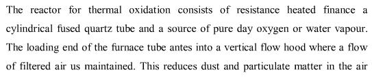
75
76
77 In lithography for micromachining, the photosensitive material used is typically a photoresist (also called resist, other photosensitive polymers are also used). When resist is exposed to a radiation source of a specific a wavelength, the chemical resistance of the resist to developer solution changes. If the resist is placed in a developer solution after selective exposure to a light source, it will etch away one of the two regions (exposed or unexposed). If the exposed material is etched away by the developer and the unexposed region is resilient, the material is considered to be a positive resist (shown in figure 2a). If the exposed material is resilient to the developer and the unexposed region is etched away, it is considered to be a negative resist (shown in figure 2b).
78 Figure 2: a) Pattern definition in positive resist, b) Pattern definition in negative resist
79

80 UNIT-2 Basic Electrical properties of MOS transistors
81
82
83
84 (b)enhancement mode device:
85
86
87
88 NMOS inverter vout
89 NMOS inverter transfer characterstic
90
91
92
93
94
95
96
97
98
99 UNIT-3
100
101
102 GND
103 CMOS design style: CMOS representations are extension of NMOS approach.
104
105

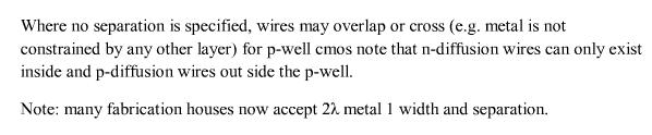
106
107
108
109 CMOS LAMDA BASED DESIGN RULES
110
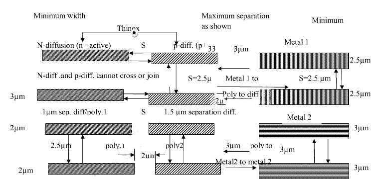
111
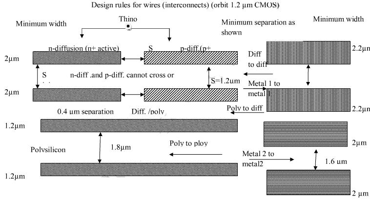
112

113
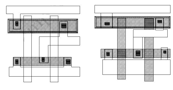
114
115 TRANSISTOR AND STICK DIAGRAM REPRESENTATION :
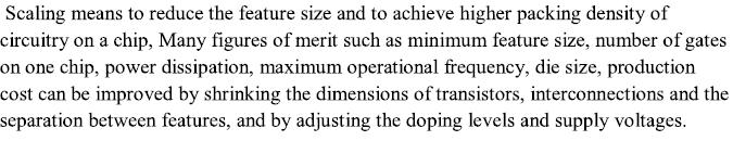
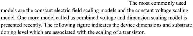
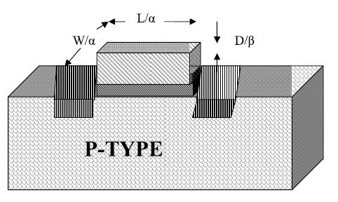
116
117
118 CURRENT DENSITY J:
119
120
121
122
123
124 UNIT-4
125
126
127
128
129

130
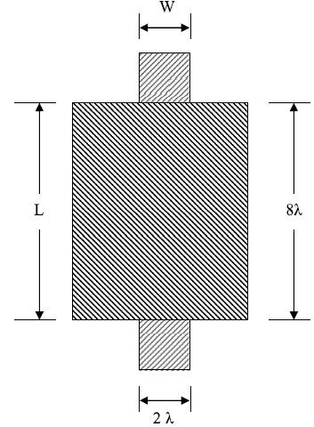
131
132
133
134
135
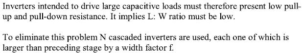
136
137
138
139
140
141
142
143 UNIT-5
144
145
146 4-bit ripple carry adder
147
148
149
150
151
152
153
154
155
156
157
158
159
160 The excitation table for 3-bit binary counter is:
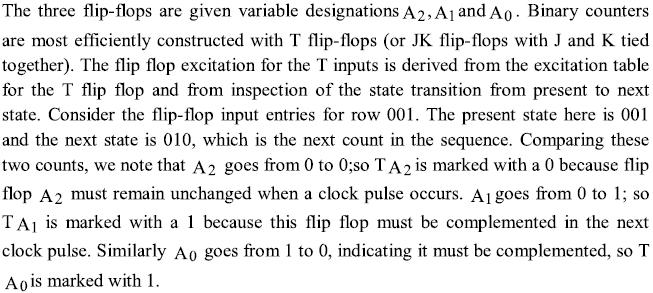
161
162
163 State diagram of the counter is shown below:
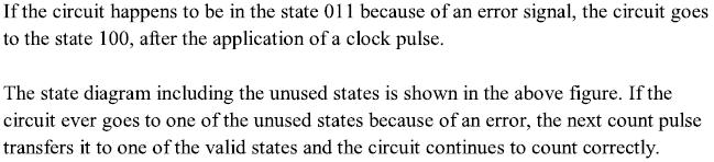
164
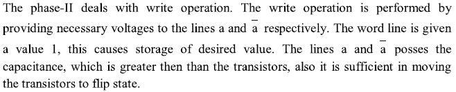
165
166
167
168
169

170 UNIT-6 PLA s:

171
172
173 Q(t+1)=JQ 1 +K 1 Q
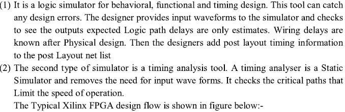
174
175 FPGA design
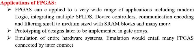
176
177
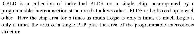
178
179
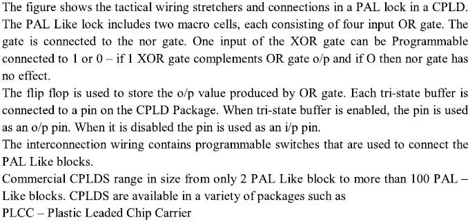
180
181
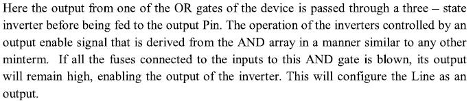
182
183
184 UNIT-7
185
186
187

188 CIRCUIT SYNTHESIS AND DESIGNFLOW:
189
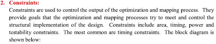
190
191 SIMULATION:
192

193
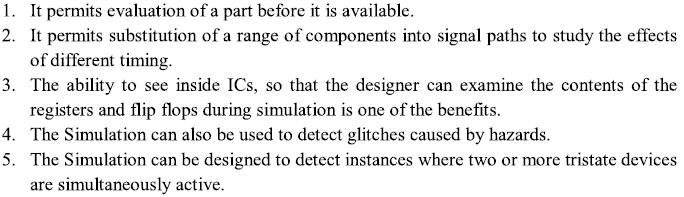
194
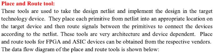
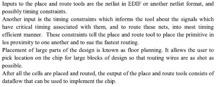
195
196
197
198
199 UNIT-8
200
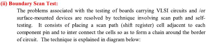
201
202
203
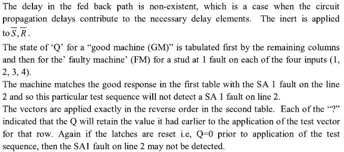
204
Figure 2.3 (cont., p. 60) (e) Block diagram of Pentium 4 processor with 42 million transistors (2000). [Courtesy Intel Corporation.
 (e) Block diagram of Pentium 4 processor with 42 million transistors (2000). [Courtesy Intel Corporation.") Figure 2.1 (p. 58) Basic fabrication steps in the silicon planar process: (a) oxide formation, (b) selective oxide removal, (c) deposition of dopant atoms on wafer, (d) diffusion of dopant atoms into exposed
Figure 2.1 (p. 58) Basic fabrication steps in the silicon planar process: (a) oxide formation, (b) selective oxide removal, (c) deposition of dopant atoms on wafer, (d) diffusion of dopant atoms into exposed
Fabrication Technology
 Fabrication Technology By B.G.Balagangadhar Department of Electronics and Communication Ghousia College of Engineering, Ramanagaram 1 OUTLINE Introduction Why Silicon The purity of Silicon Czochralski
CMOS FABRICATION. n WELL PROCESS
 CMOS FABRICATION n WELL PROCESS Step 1: Si Substrate Start with p- type substrate p substrate Step 2: Oxidation Exposing to high-purity oxygen and hydrogen at approx. 1000 o C in oxidation furnace SiO
EE40 Lec 22. IC Fabrication Technology. Prof. Nathan Cheung 11/19/2009
 Suggested Reading EE40 Lec 22 IC Fabrication Technology Prof. Nathan Cheung 11/19/2009 300mm Fab Tour http://www-03.ibm.com/technology/manufacturing/technology_tour_300mm_foundry.html Overview of IC Technology
VLSI Technology. By: Ajay Kumar Gautam
 By: Ajay Kumar Gautam Introduction to VLSI Technology, Crystal Growth, Oxidation, Epitaxial Process, Diffusion Process, Ion Implantation, Lithography, Etching, Metallization, VLSI Process Integration,
Silicon Wafer Processing PAKAGING AND TEST
 Silicon Wafer Processing PAKAGING AND TEST Parametrical test using test structures regularly distributed in the wafer Wafer die test marking defective dies dies separation die fixing (not marked as defective)
Lecture 030 Integrated Circuit Technology - I (5/8/03) Page 030-1
 Page 030-1") Lecture 030 Integrated Circuit Technology - I (5/8/03) Page 030-1 LECTURE 030 INTEGRATED CIRCUIT TECHNOLOGY - I (References [7,8]) Objective The objective of this presentation is: 1.) Illustrate integrated
Lecture 030 Integrated Circuit Technology - I (5/8/03) Page 030-1 LECTURE 030 INTEGRATED CIRCUIT TECHNOLOGY - I (References [7,8]) Objective The objective of this presentation is: 1.) Illustrate integrated
Lecture 19 Microfabrication 4/1/03 Prof. Andy Neureuther
 EECS 40 Spring 2003 Lecture 19 Microfabrication 4/1/03 Prof. ndy Neureuther How are Integrated Circuits made? Silicon wafers Oxide formation by growth or deposition Other films Pattern transfer by lithography
KGC SCIENTIFIC Making of a Chip
 KGC SCIENTIFIC www.kgcscientific.com Making of a Chip FROM THE SAND TO THE PACKAGE, A DIAGRAM TO UNDERSTAND HOW CPU IS MADE? Sand CPU CHAIN ANALYSIS OF SEMICONDUCTOR Material for manufacturing process
Ajay Kumar Gautam [VLSI TECHNOLOGY] VLSI Technology for 3RD Year ECE/EEE Uttarakhand Technical University
![Ajay Kumar Gautam [VLSI TECHNOLOGY] VLSI Technology for 3RD Year ECE/EEE Uttarakhand Technical University](/thumbs/75/72824557.jpg "Ajay Kumar Gautam [VLSI TECHNOLOGY] VLSI Technology for 3RD Year ECE/EEE Uttarakhand Technical University") 2014 Ajay Kumar Gautam [VLSI TECHNOLOGY] VLSI Technology for 3RD Year ECE/EEE Uttarakhand Technical University Page1 Syllabus UNIT 1 Introduction to VLSI Technology: Classification of ICs, Scale of integration,
2014 Ajay Kumar Gautam [VLSI TECHNOLOGY] VLSI Technology for 3RD Year ECE/EEE Uttarakhand Technical University Page1 Syllabus UNIT 1 Introduction to VLSI Technology: Classification of ICs, Scale of integration,
PROCESSING OF INTEGRATED CIRCUITS
 PROCESSING OF INTEGRATED CIRCUITS Overview of IC Processing (Part I) Silicon Processing Lithography Layer Processes Use in IC Fabrication (Part II) Integrating the Fabrication Steps IC Packaging (Part
Isolation Technology. Dr. Lynn Fuller
 ROCHESTER INSTITUTE OF TECHNOLOGY MICROELECTRONIC ENGINEERING Isolation Technology Dr. Lynn Fuller Motorola Professor 82 Lomb Memorial Drive Rochester, NY 14623-5604 Tel (585) 475-2035 Fax (585) 475-5041
Intel Pentium Processor W/MMX
 Construction Analysis Intel Pentium Processor W/MMX Report Number: SCA 9706-540 Global Semiconductor Industry the Serving Since 1964 15022 N. 75th Street Scottsdale, AZ 85260-2476 Phone: 602-998-9780 Fax:
National Semiconductor LM2672 Simple Switcher Voltage Regulator
 Construction Analysis National Semiconductor LM2672 Simple Switcher Voltage Regulator Report Number: SCA 9712-570 Global Semiconductor Industry the Serving Since 1964 17350 N. Hartford Drive Scottsdale,
3.155J / 6.152J Micro/Nano Processing Technology TAKE-HOME QUIZ FALL TERM 2005
 3.155J / 6.152J Micro/Nano Processing Technology TAKE-HOME QUIZ FALL TERM 2005 1) This is an open book, take-home quiz. You are not to consult with other class members or anyone else. You may discuss the
CMOS Manufacturing process. Circuit designer. Design rule set. Process engineer. Set of optical masks. Fabrication process.
 CMOS Manufacturing process Circuit design Set of optical masks Fabrication process Circuit designer Design rule set Process engineer All material: Chap. 2 of J. Rabaey, A. Chandrakasan, B. Nikolic, Digital
CHAPTER 1 HOW SEMICONDUCTOR CHIPS ARE MADE
 CHAPTER 1 HOW SEMICONDUCTOR CHIPS ARE MADE Hwaiyu Geng Hewlett-Packard Company Palo Alto, California Lin Zhou Intel Corporation Hillsboro, Oregon 1.1 INTRODUCTION Over the past decades, an information
Section 4: Thermal Oxidation. Jaeger Chapter 3. EE143 - Ali Javey
 Section 4: Thermal Oxidation Jaeger Chapter 3 Properties of O Thermal O is amorphous. Weight Density =.0 gm/cm 3 Molecular Density =.3E molecules/cm 3 O Crystalline O [Quartz] =.65 gm/cm 3 (1) Excellent
Motorola PC603R Microprocessor
 Construction Analysis Motorola PC603R Microprocessor Report Number: SCA 9709-551 Global Semiconductor Industry the Serving Since 1964 17350 N. Hartford Drive Scottsdale, AZ 85255 Phone: 602-515-9780 Fax:
Process Flow in Cross Sections
 Process Flow in Cross Sections Process (simplified) 0. Clean wafer in nasty acids (HF, HNO 3, H 2 SO 4,...) --> wear gloves! 1. Grow 500 nm of SiO 2 (by putting the wafer in a furnace with O 2 2. Coat
Radiation Tolerant Isolation Technology
 Radiation Tolerant Isolation Technology Background The following contains a brief description of isolation technologies used for radiation hardened integrated circuits. The technologies mentioned are junction
Cost of Integrated Circuits
 Cost of IC Design 1 Cost of Integrated Circuits NRE (Non-Recurrent Engineering) costs fixed design time and effort, mask generation independent of sales volume / number of products one-time cost factor
Lecture 4. Oxidation (applies to Si and SiC only) Reading: Chapter 4
 Reading: Chapter 4") Lecture 4 Oxidation (applies to Si and SiC only) Reading: Chapter 4 Introduction discussion: Oxidation: Si (and SiC) Only The ability to grow a high quality thermal oxide has propelled Si into the forefront
Lecture 4 Oxidation (applies to Si and SiC only) Reading: Chapter 4 Introduction discussion: Oxidation: Si (and SiC) Only The ability to grow a high quality thermal oxide has propelled Si into the forefront
VLSI Technology Dr. Nandita Dasgupta Department of Electrical Engineering Indian Institute of Technology, Madras
 VLSI Technology Dr. Nandita Dasgupta Department of Electrical Engineering Indian Institute of Technology, Madras Lecture - 33 Problems in LOCOS + Trench Isolation and Selective Epitaxy So, we are discussing
Historical Development. Babbage s second computer. Before the digital age
 Historical Development To fully appreciate the computers of today, it is helpful to understand how things got the way they are The evolution of computing machinery has taken place over several centuries
VLSI Systems and Computer Architecture Lab
 ΚΥΚΛΩΜΑΤΑ VLSI Πανεπιστήμιο Ιωαννίνων CMOS Technology Τμήμα Μηχανικών Η/Υ και Πληροφορικής 1 From the book: An Introduction ti to VLSI Process By: W. Maly ΚΥΚΛΩΜΑΤΑ VLSI Διάρθρωση 1. N well CMOS 2. Active
Semiconductor Manufacturing Technology. IC Fabrication Process Overview
 Semiconductor Manufacturing Technology Michael Quirk & Julian Serda October 00 by Prentice Hall Chapter 9 IC Fabrication Process Overview /4 Objectives After studying the material in this chapter, you
Dallas Semicoductor DS80C320 Microcontroller
 Construction Analysis Dallas Semicoductor DS80C320 Microcontroller Report Number: SCA 9702-525 Global Semiconductor Industry the Serving Since 1964 15022 N. 75th Street Scottsdale, AZ 85260-2476 Phone:
CMOS Manufacturing Process
 CMOS Manufacturing Process CMOS Process A Modern CMOS Process gate-oxide TiSi 2 AlCu Tungsten SiO 2 n+ p-well p-epi poly n-well p+ SiO 2 p+ Dual-Well Trench-Isolated CMOS Process Circuit Under Design V
Thermal Evaporation. Theory
 Thermal Evaporation Theory 1. Introduction Procedures for depositing films are a very important set of processes since all of the layers above the surface of the wafer must be deposited. We can classify
Oxide Growth. 1. Introduction
 Oxide Growth 1. Introduction Development of high-quality silicon dioxide (SiO2) has helped to establish the dominance of silicon in the production of commercial integrated circuits. Among all the various
Rockwell R RF to IF Down Converter
 Construction Analysis Rockwell R6732-13 RF to IF Down Converter Report Number: SCA 9709-552 Global Semiconductor Industry the Serving Since 1964 17350 N. Hartford Drive Scottsdale, AZ 85255 Phone: 602-515-9780
Today s agenda (19-JAN-2010)
") Today s agenda (19-JAN-2010) 1) Overview of Integrated Circuit technology 2) Managing Deadlines 3) A look @ Spring Schedule 4) Suggested milestones 5) Project concept presentations Action items from last
Today s agenda (19-JAN-2010) 1) Overview of Integrated Circuit technology 2) Managing Deadlines 3) A look @ Spring Schedule 4) Suggested milestones 5) Project concept presentations Action items from last
Section 4: Thermal Oxidation. Jaeger Chapter 3
 Section 4: Thermal Oxidation Jaeger Chapter 3 Properties of O Thermal O is amorphous. Weight Density =.0 gm/cm 3 Molecular Density =.3E molecules/cm 3 O Crystalline O [Quartz] =.65 gm/cm 3 (1) Excellent
1. Introduction. What is implantation? Advantages
 Ion implantation Contents 1. Introduction 2. Ion range 3. implantation profiles 4. ion channeling 5. ion implantation-induced damage 6. annealing behavior of the damage 7. process consideration 8. comparison
Metallization deposition and etching. Material mainly taken from Campbell, UCCS
 Metallization deposition and etching Material mainly taken from Campbell, UCCS Application Metallization is back-end processing Metals used are aluminum and copper Mainly involves deposition and etching,
Etching Etching Definitions Isotropic Etching: same in all direction Anisotropic Etching: direction sensitive Selectivity: etch rate difference
 Etching Etching Definitions Isotropic Etching: same in all direction Anisotropic Etching: direction sensitive Selectivity: etch rate difference between 2 materials Need strong selectivity from masking
CMOS VLSI Design M.Tech. First semester VTU Anil V. Nandi, ECE department, BVBCET, Hubli
 CMOS VLSI Design M.Tech. First semester VTU Anil V. Nandi, ECE department, BVBCET, Hubli-580031. Contents: Semiconductor Technology overview Silicon Growth/Processing,Oxidation, Diffusion, Epitaxy, deposition,
LANDOLT-BÖRNSTEIN. Zahlenwerte und Funktionen aus Naturwissenschaften und Technik. Neue Serie. Gesamtherausgabe: K.-H. Hellwege O.
 LANDOLT-BÖRNSTEIN Zahlenwerte und Funktionen aus Naturwissenschaften und Technik Neue Serie Gesamtherausgabe: K.-H. Hellwege O. Madelung Gruppe III: Kristall- und Festkörperphysik Band 17 Halbleiter Herausgeber:
Technology. Semiconductor Manufacturing. Hong Xiao INTRODUCTION TO SECOND EDITION SPIE PRESS
 INTRODUCTION TO Semiconductor Manufacturing Technology SECOND EDITION Hong Xiao TECHNISCHE INFORMATIONSBiBUOTHEK UNIVERSITATSBIBLIOTHEK HANNOVER SPIE PRESS Bellingham,Washington USA Contents Preface to
SGS-Thomson M17C1001 1Mb UVEPROM
 Construction Analysis SGS-Thomson M17C1001 1Mb UVEPROM Report Number: SCA 9612-518 Global Semiconductor Industry the Serving Since 1964 15022 N. 75th Street Scottsdale, AZ 85260-2476 Phone: 602-998-9780
Surface micromachining and Process flow part 1
 Surface micromachining and Process flow part 1 Identify the basic steps of a generic surface micromachining process Identify the critical requirements needed to create a MEMS using surface micromachining
Hitachi A 64Mbit (8Mb x 8) Dynamic RAM
 Dynamic RAM") Construction Analysis Hitachi 5165805A 64Mbit (8Mb x 8) Dynamic RAM Report Number: SCA 9712-565 Global Semiconductor Industry the Serving Since 1964 17350 N. Hartford Drive Scottsdale, AZ 85255 Phone:
Construction Analysis Hitachi 5165805A 64Mbit (8Mb x 8) Dynamic RAM Report Number: SCA 9712-565 Global Semiconductor Industry the Serving Since 1964 17350 N. Hartford Drive Scottsdale, AZ 85255 Phone:
EE-612: Lecture 28: Overview of SOI Technology
 EE-612: Lecture 28: Overview of SOI Technology Mark Lundstrom Electrical and Computer Engineering Purdue University West Lafayette, IN USA Fall 2006 NCN www.nanohub.org Lundstrom EE-612 F06 1 outline 1)
Lab #2 Wafer Cleaning (RCA cleaning)
") Lab #2 Wafer Cleaning (RCA cleaning) RCA Cleaning System Used: Wet Bench 1, Bay1, Nanofabrication Center Chemicals Used: H 2 O : NH 4 OH : H 2 O 2 (5 : 1 : 1) H 2 O : HF (10 : 1) H 2 O : HCl : H 2 O 2
Lab #2 Wafer Cleaning (RCA cleaning) RCA Cleaning System Used: Wet Bench 1, Bay1, Nanofabrication Center Chemicals Used: H 2 O : NH 4 OH : H 2 O 2 (5 : 1 : 1) H 2 O : HF (10 : 1) H 2 O : HCl : H 2 O 2
Plasma Etching Rates & Gases Gas ratios affects etch rate & etch ratios to resist/substrate
 Plasma Etching Rates & Gases Gas ratios affects etch rate & etch ratios to resist/substrate Development of Sidewalls Passivating Films Sidewalls get inert species deposited on them with plasma etch Creates
R Sensor resistance (Ω) ρ Specific resistivity of bulk Silicon (Ω cm) d Diameter of measuring point (cm)
 ρ Specific resistivity of bulk Silicon (Ω cm) d Diameter of measuring point (cm)") 4 Silicon Temperature Sensors 4.1 Introduction The KTY temperature sensor developed by Infineon Technologies is based on the principle of the Spreading Resistance. The expression Spreading Resistance derives
4 Silicon Temperature Sensors 4.1 Introduction The KTY temperature sensor developed by Infineon Technologies is based on the principle of the Spreading Resistance. The expression Spreading Resistance derives
Semiconductor Technology
 Semiconductor Technology von A bis Z Metallization www.halbleiter.org Contents Contents List of Figures List of Tables II III 1 Metallization 1 1.1 Requirements on metallization........................
Lecture Day 2 Deposition
 Deposition Lecture Day 2 Deposition PVD - Physical Vapor Deposition E-beam Evaporation Thermal Evaporation (wire feed vs boat) Sputtering CVD - Chemical Vapor Deposition PECVD LPCVD MVD ALD MBE Plating
ME 141B: The MEMS Class Introduction to MEMS and MEMS Design. Sumita Pennathur UCSB
 ME 141B: The MEMS Class Introduction to MEMS and MEMS Design Sumita Pennathur UCSB Outline today Introduction to thin films Oxidation Deal-grove model CVD Epitaxy Electrodeposition 10/6/10 2/45 Creating
BASICS OF MANUFACTURING INTEGRATED CIRCUITS
 BASICS OF MANUFACTURING INTEGRATED CIRCUITS Opportunities for filtration exist for the manufacture of very small electronic components referred to as semiconductors. This broad category includes devices
Semiconductor Device Fabrication Study
 Proceedings of The National Conference on Undergraduate Research (NCUR) 2003 University of Utah, Salt Lake City, Utah March 13-15, 2003 Semiconductor Device Fabrication Study Tsung-Ta Ho and Michael R.
Supporting Information
 Supporting Information Fast-Response, Sensitivitive and Low-Powered Chemosensors by Fusing Nanostructured Porous Thin Film and IDEs-Microheater Chip Zhengfei Dai,, Lei Xu,#,, Guotao Duan *,, Tie Li *,,
Ultra High Barrier Coatings by PECVD
 Society of Vacuum Coaters 2014 Technical Conference Presentation Ultra High Barrier Coatings by PECVD John Madocks & Phong Ngo, General Plasma Inc., 546 E. 25 th Street, Tucson, Arizona, USA Abstract Silicon
Surface Micromachining
 Surface Micromachining Outline Introduction Material often used in surface micromachining Material selection criteria in surface micromachining Case study: Fabrication of electrostatic motor Major issues
Lecture 12. Physical Vapor Deposition: Evaporation and Sputtering Reading: Chapter 12. ECE Dr. Alan Doolittle
 Lecture 12 Physical Vapor Deposition: Evaporation and Sputtering Reading: Chapter 12 Evaporation and Sputtering (Metalization) Evaporation For all devices, there is a need to go from semiconductor to metal.
Leveraging the Precision of Electroforming over Alternative Processes When Developing Nano-scale Structures
 VOLUME 4 - ELECTROFORMING Leveraging the Precision of over Alternative Processes When Developing Nano-scale Structures Electrical and mechanical component and subsystem designers generally have five techniques
MARORA A Plasma Selective-oxidation Apparatus for Metal-gate Devices
 Hitachi Review Vol. 57 (2008), No. 3 127 MARORA A Plasma Selective-oxidation Apparatus for Metal-gate Devices Tadashi Terasaki Masayuki Tomita Katsuhiko Yamamoto Unryu Ogawa, Dr. Eng. Yoshiki Yonamoto,
Isolation of elements
 1 In an IC, devices on the same substrate must be isolated from one another so that there is no current conduction between them. Isolation uses either the junction or dielectric technique or a combination
Chapter 1.6. Polished Single-Crystal Silicon, Prime Wafers (all numbers nominal) Wafer Specification Table. Diameter 100 mm 4-inch 150 mm 6-inch
 Wafer Specification Table. Diameter 100 mm 4-inch 150 mm 6-inch") Chapter 1.6 I - Substrate Specifications Polished Single-Crystal Silicon, Prime Wafers (all numbers nominal) Wafer Specification Table Diameter 100 mm 4-inch 150 mm 6-inch Thickness 525 µm 20.5 mils 675
Chapter 1.6 I - Substrate Specifications Polished Single-Crystal Silicon, Prime Wafers (all numbers nominal) Wafer Specification Table Diameter 100 mm 4-inch 150 mm 6-inch Thickness 525 µm 20.5 mils 675
Schottky-Barrier-Height Modulation of Ni Silicide/Si Contacts by Insertion of Thin Er or Pt Layers
 Schottky-Barrier-Height Modulation of Ni Silicide/Si Contacts by Insertion of Thin Er or Pt Layers Yoshihisa Ohishi 1, Kohei Noguchi 1, Kuniyuki Kakushima 2, Parhat Ahmet 1, Kazuo Tsutsui 2, Nobuyuki Sugii
From microelectronics down to nanotechnology.
 From microelectronics down to nanotechnology sami.franssila@tkk.fi Contents Lithography: scaling x- and y-dimensions MOS transistor physics Scaling oxide thickness (z-dimension) CNT transistors Conducting
Advanced CMOS Process Technology Part 3 Dr. Lynn Fuller
 MICROELECTRONIC ENGINEERING ROCHESTER INSTITUTE OF TECHNOLOGY Part 3 Dr. Lynn Fuller Webpage: http://people.rit.edu/lffeee Electrical and Microelectronic Engineering Rochester Institute of Technology 82
id : class06 passwd: class06
 http://wwwee.stanford.edu/class_directory.php http://ocw.mit.edu/ocwweb/index.htm http://nanosioe.ee.ntu.edu.tw id : class06 passwd: class06 Display and OLED Market OLED on glass only ~US$ 0.5B in 04,
Modeling of Local Oxidation Processes
 Introduction Isolation Processes in the VLSI Technology Main Aspects of LOCOS simulation Athena Oxidation Models Several Examples of LOCOS structures Calibration of LOCOS effects using VWF Field Oxide
Microstructures using RF sputtered PSG film as a sacrificial layer in surface micromachining
 Sādhanā Vol. 34, Part 4, August 2009, pp. 557 562. Printed in India Microstructures using RF sputtered PSG film as a sacrificial layer in surface micromachining VIVEKANAND BHATT 1,, SUDHIR CHANDRA 1 and
Interconnects. Outline. Interconnect scaling issues Aluminum technology Copper technology. Properties of Interconnect Materials
 Interconnects Outline Interconnect scaling issues Aluminum technology Copper technology 1 Properties of Interconnect Materials Metals Silicides Barriers Material Thin film Melting resistivity point ( C)
Lezioni di Tecnologie e Materiali per l Elettronica
 Lezioni di Tecnologie e Materiali er l Elettronica Danilo Manstretta danilo.manstretta@univ.it microlab.univ.it Outline Passive comonents Resistors Caacitors Inductors Printed circuits technologies Materials
Silicon Oxides: SiO 2
 Silicon Oxides: SiO 2 Uses: diffusion masks surface passivation gate insulator (MOSFET) isolation, insulation Formation: grown / native thermal: highest quality anodization deposited: C V D, evaporate,
2006 UPDATE METROLOGY
 INTERNATIONAL TECHNOLOGY ROADMAP FOR SEMICONDUCTORS METROLOGY THE ITRS DEVED AND INTENDED FOR TECHNOLOGY ASSESSMENT ONLY AND WITHOUT REGARD TO ANY COMMERCIAL CONSIDERATIONS PERTAINING TO INDIVIDUAL PRODUCTS
Cu Wiring Process for TFTs - Improved Hydrogen Plasma Resistance with a New Cu Alloy -
 Cu Wiring Process for TFTs - Improved Hydrogen Plasma Resistance with a New Cu Alloy - Masanori Shirai*, Satoru Takazawa*, Satoru Ishibashi*, Tadashi Masuda* As flat-screen TVs become larger and their
Atomic Layer Deposition(ALD)
") Atomic Layer Deposition(ALD) AlO x for diffusion barriers OLED displays http://en.wikipedia.org/wiki/atomic_layer_deposition#/media/file:ald_schematics.jpg Lam s market-leading ALTUS systems combine CVD
Atomic Layer Deposition(ALD) AlO x for diffusion barriers OLED displays http://en.wikipedia.org/wiki/atomic_layer_deposition#/media/file:ald_schematics.jpg Lam s market-leading ALTUS systems combine CVD
Development of a Deep-Submicron CMOS Process for Fabrication of High Performance 0.25 mm Transistors
 Development of a Deep-Submicron CMOS Process for Fabrication of High Performance 0.25 mm Transistors Michael Aquilino M.S. Thesis Defense Department May 19, 2006 Motivation o Enable the department to continue
Silicon Wafers: Basic unit Silicon Wafers Basic processing unit 100, 150, 200, 300, 450 mm disk, mm thick Current industrial standard 300 mm
 Silicon Wafers: Basic unit Silicon Wafers Basic processing unit 100, 150, 200, 300, 450 mm disk, 0.5-0.8 mm thick Current industrial standard 300 mm (12 inches) Most research labs 100, 150 mm wafers (ours
Plasma-Enhanced Chemical Vapor Deposition
 Plasma-Enhanced Chemical Vapor Deposition Steven Glenn July 8, 2009 Thin Films Lab 4 ABSTRACT The objective of this lab was to explore lab and the Applied Materials P5000 from a different point of view.
5.8 Diaphragm Uniaxial Optical Accelerometer
 5.8 Diaphragm Uniaxial Optical Accelerometer Optical accelerometers are based on the BESOI (Bond and Etch back Silicon On Insulator) wafers, supplied by Shin-Etsu with (100) orientation, 4 diameter and
State of the art quality of a GeOx interfacial passivation layer formed on Ge(001)
") APPLICATION NOTE State of the art quality of a Ox interfacial passivation layer formed on (001) Summary A number of research efforts have been made to realize Metal-Oxide-Semiconductor Field Effect Transistors
APPLICATION NOTE State of the art quality of a Ox interfacial passivation layer formed on (001) Summary A number of research efforts have been made to realize Metal-Oxide-Semiconductor Field Effect Transistors
Long-term reliability of SiC devices. Power and Hybrid
 Long-term reliability of SiC devices Power and Hybrid Rob Coleman Business Development and Applications Manager TT electronics, Power and Hybrid Roger Tall Product Specialist Charcroft Electronics Ltd
Alternative Methods of Yttria Deposition For Semiconductor Applications. Rajan Bamola Paul Robinson
 Alternative Methods of Yttria Deposition For Semiconductor Applications Rajan Bamola Paul Robinson Origin of Productivity Losses in Etch Process Aggressive corrosive/erosive plasma used for etch Corrosion/erosion
Photolithography I ( Part 2 )
") 1 Photolithography I ( Part 2 ) Chapter 13 : Semiconductor Manufacturing Technology by M. Quirk & J. Serda Bjørn-Ove Fimland, Department of Electronics and Telecommunication, Norwegian University of Science
1 Photolithography I ( Part 2 ) Chapter 13 : Semiconductor Manufacturing Technology by M. Quirk & J. Serda Bjørn-Ove Fimland, Department of Electronics and Telecommunication, Norwegian University of Science
Applications of High-Performance MEMS Pressure Sensors Based on Dissolved Wafer Process
 Applications of High-Performance MEMS Pressure Sensors Based on Dissolved Wafer Process Srinivas Tadigadapa and Sonbol Massoud-Ansari Integrated Sensing Systems (ISSYS) Inc., 387 Airport Industrial Drive,
UTILIZATION OF ATMOSPHERIC PLASMA SURFACE PREPARATION TO IMPROVE COPPER PLATING PROCESSES.
 SESSION 14 MATERIALS AND PROCESSES FOR ADVANCED PACKAGING UTILIZATION OF ATMOSPHERIC PLASMA SURFACE PREPARATION TO IMPROVE COPPER PLATING PROCESSES. Eric Schulte 1, Gilbert Lecarpentier 2 SETNA Corporation
NON-PLANAR SILICON OXIDATION: AN EXTENSION OF THE DEAL-GROVE MODEL BRIAN D. LEMME. B.S., University of Nebraska-Lincoln, 2000 A REPORT
 NON-PLANAR SILICON OXIDATION: AN EXTENSION OF THE DEAL-GROVE MODEL by BRIAN D. LEMME B.S., University of Nebraska-Lincoln, 2000 A REPORT submitted in partial fulfillment of the requirements for the degree
HBLED packaging is becoming one of the new, high
 Ag plating in HBLED packaging improves reflectivity and lowers costs JONATHAN HARRIS, President, CMC Laboratories, Inc., Tempe, AZ Various types of Ag plating technology along with the advantages and limitations
Materials for MEMS. Dr. Yael Hanein. 11 March 2004 Materials Applications Yael Hanein
 Materials for MEMS Dr. Yael Hanein Materials for MEMS MEMS (introduction) Materials used in MEMS Material properties Standard MEMS processes MEMS The world s smallest guitar is about 10 micrometers long
How To Write A Flowchart
 1 Learning Objectives To learn how you transfer a device concept into a process flow to fabricate the device in the EKL labs You learn the different components that makes up a flowchart; process blocks,
EXCIMER LASER ANNEALING FOR LOW- TEMPERATURE POLYSILICON THIN FILM TRANSISTOR FABRICATION ON PLASTIC SUBSTRATES
 EXCIMER LASER ANNEALING FOR LOW- TEMPERATURE POLYSILICON THIN FILM TRANSISTOR FABRICATION ON PLASTIC SUBSTRATES G. Fortunato, A. Pecora, L. Maiolo, M. Cuscunà, D. Simeone, A. Minotti, and L. Mariucci CNR-IMM,
Electrical Properties of Ultra Shallow p Junction on n type Si Wafer Using Decaborane Ion Implantation
 Mat. Res. Soc. Symp. Proc. Vol. 686 2002 Materials Research Society Electrical Properties of Ultra Shallow p Junction on n type Si Wafer Using Decaborane Ion Implantation Jae-Hoon Song, Duck-Kyun Choi
ME 189 Microsystems Design and Manufacture. Chapter 9. Micromanufacturing
 ME 189 Microsystems Design and Manufacture Chapter 9 Micromanufacturing This chapter will offer an overview of the application of the various fabrication techniques described in Chapter 8 in the manufacturing
IEEE TRANSACTIONS ON NUCLEAR SCIENCE, VOL. 55, NO. 4, AUGUST
 IEEE TRANSACTIONS ON NUCLEAR SCIENCE, VOL. 55, NO. 4, AUGUST 2008 1833 Radiation Effects in MOS Oxides James R. Schwank, Fellow, IEEE, Marty R. Shaneyfelt, Fellow, IEEE, Daniel M. Fleetwood, Fellow, IEEE,
Chapter 2. Density 2.65 g/cm 3 Melting point Young s modulus Tensile strength Thermal conductivity Dielectric constant 3.
 Chapter 2 Thin Film Materials Thin films of Silicon dioxide, Silicon nitride and Polysilicon have been utilized in the fabrication of absolute micro pressure sensor. These materials are studied and discussed
THE MANUFACTURING PROCESS
 chapter2.fm Page 33 Monday, September 4, 2000 11:11 AM CHAPTER 2 THE MANUFACTURING PROCESS Overview of manufacturing process n Design rules n IC packaging n Future Trends in Integrated Circuit Technology
Amorphous Oxide Transistor Electrokinetic Reflective Display on Flexible Glass
 Amorphous Oxide Transistor Electrokinetic Reflective Display on Flexible Glass Devin A. Mourey, Randy L. Hoffman, Sean M. Garner *, Arliena Holm, Brad Benson, Gregg Combs, James E. Abbott, Xinghua Li*,
Rapid Thermal Processing (RTP) Dr. Lynn Fuller
 Dr. Lynn Fuller") ROCHESTER INSTITUTE OF TECHNOLOGY MICROELECTRONIC ENGINEERING Rapid Thermal Processing (RTP) Dr. Lynn Fuller Webpage: http://people.rit.edu/lffeee 82 Lomb Memorial Drive Rochester, NY 14623-5604 Tel (585)
ROCHESTER INSTITUTE OF TECHNOLOGY MICROELECTRONIC ENGINEERING Rapid Thermal Processing (RTP) Dr. Lynn Fuller Webpage: http://people.rit.edu/lffeee 82 Lomb Memorial Drive Rochester, NY 14623-5604 Tel (585)
Implant Metrology for Bonded SOI Wafers Using a Surface Photo-Voltage Technique
 Implant Metrology for Bonded SOI Wafers Using a Surface Photo-Voltage Technique Adam Bertuch a, Wesley Smith a, Ken Steeples a, Robert Standley b, Anca Stefanescu b, and Ron Johnson c a QC Solutions Inc.,
EE C245 ME C218 Introduction to MEMS Design Fall 2011
 Lecture Outline EE C245 ME C218 Introduction to MEMS Design Fall 2011 Prof. Clark T.-C. Nguyen Dept. of Electrical Engineering & Computer Sciences University of California at Berkeley Berkeley, CA 94720
Welding Processes. Consumable Electrode. Non-Consumable Electrode. High Energy Beam. Fusion Welding Processes. SMAW Shielded Metal Arc Welding
 Fusion Consumable Electrode SMAW Shielded Metal Arc Welding GMAW Gas Metal Arc Welding SAW Submerged Arc Welding Non-Consumable Electrode GTAW Gas Tungsten Arc Welding PAW Plasma Arc Welding High Energy
Report 1. B. Starting Wafer Specs Number: 10 Total, 6 Device and 4 Test wafers
 Aaron Pederson EE 432 Lab Dr. Meng Lu netid: abp250 Lab instructor: Yunfei Zhao Report 1 A. Overview The goal of this lab is to go through the semiconductor fabrication process from start to finish. This
BONDING OF MULTIPLE WAFERS FOR HIGH THROUGHPUT LED PRODUCTION. S. Sood and A. Wong
 10.1149/1.2982882 The Electrochemical Society BONDING OF MULTIPLE WAFERS FOR HIGH THROUGHPUT LED PRODUCTION S. Sood and A. Wong Wafer Bonder Division, SUSS MicroTec Inc., 228 SUSS Drive, Waterbury Center,
SPI Supplies Brand MgO Magnesium Oxide Single Crystal Substrates, Blocks, and Optical Components
 SPI Supplies Brand MgO Magnesium Oxide Single Crystal Substrates, Blocks, and Optical Components Used by high temperature thin film superconductor researchers worldwide! Purity better than 99.9%! Choose