Detectors and Coatings for Efficient Systems for Future UV Astronomy
|
|
|
- Ashlynn Garrison
- 6 years ago
- Views:
Transcription


1 Detectors and Coatings for Efficient Systems for Future UV Astronomy John Hennessy M. E. Hoenk, A. Carver, T.J. Jones, A. Jewell, E. Hamden, T. Goodsall, S. Nikzad Jet Propulsion Laboratory, California Institute of Technology ESO/NUVA/IAG Workshop on Challenges in UV Astronomy ESO Garching, 7-11 October California Institute of Technology. Government sponsorship acknowledged.
2
3 Outline High Performance Silicon Detectors through Atomic-scale surface/interface engineering Enables high efficiency, stable response, and reliable performance Delta doping plus ALD AR coatings Wafer Scale Processing for High Throughput and High Yield Large scale, high throughput, high yield production for mission applications Wafer scale devices (taking up the entire 8-inch wafer area) Examples of Recent Devices and Application FUV EMCCD (FIREBall) UV P-channel CCDs (CHESS) Broadband (WaSP) Work on Reflective Optical Coatings via ALD


4 High Performance Silicon Imaging through Back-illumination Key detector performance parameters depend on back illumination for all silicon imaging devices. Back illumination allows absorption of photons in silicon active area and near the collection well These key parameters include wide spectral range, efficiency, resolution, stability of response, dark current, and high fill factor Several 100 Å of poly silicon and oxide prevent absorption of UV photons into the device Si Detector: Energy Band Cross-section Front illumination Back illumination Back Front
 Bandstructure engineering for optimum device performance with atomic layer control over silicon surface original Si ~ 15 µm Native oxide 0.")
5 Delta doping technology via MBE µm Delta-doped layer (boron in single atomic layer) Bandstructure engineering for optimum device performance with atomic layer control over silicon surface original Si ~ 15 µm Native oxide µm Thinned CCD CCD frontside circuitry Low temperature process, compatible with VLSI, fully - fabricated devices (CCDs, CMOS, PIN arrays) Hoenk et al., Applied Physics Letters, 61: 1084 (1992)


6 100% Internal QE with Delta doping through Atomically Precise Interface Engineering Quantum Efficiency of Delta doped CCDs 100% internal quantum efficiency, uniform, and stable (QY has been removed so maximum QE is 100%). Extreme UV measurements were made at SSRL Compatible with AR and filter coating: response can be tailored for different regions of the spectrum
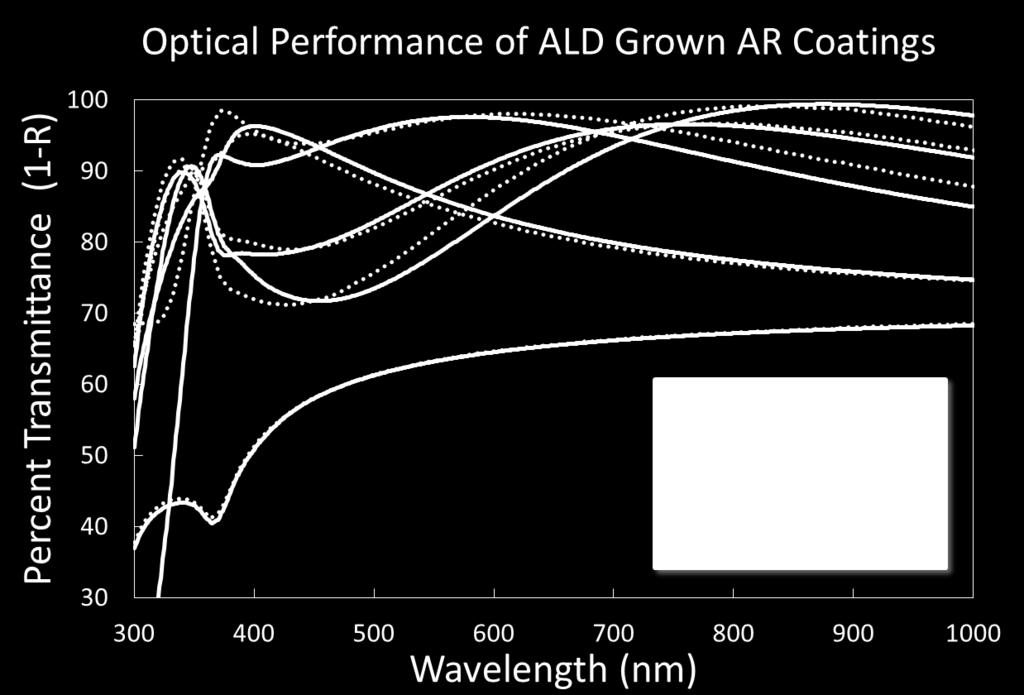
7 QE (%) > 50% External Quantum Efficiency Achieved in UV Bare MgF 2 13 nm Al 2 O 3 16 nm Al 2 O 3 23 nm HfO 2 23 nm GALEX FUV GALEX NUV Wavelength (nm) Delta doping & Atomic Layer Deposition of standard CCDs & EMCCDs Nikzad, et al. Applied Optics, 2012


8 High External QE with Atomic Layer Deposition through Atomically Precise Interface Engineering What is ALD? Surface reaction mediated deposition ALD cycles are repeated until desired film thickness is achieved Metals, Nitrides, and Oxides are achieved through choice of precursor and reactant species Can achieve thin film deposition or surface modifications at near room temperature Results in smooth, stoichiometric, thin layers. Abrupt interfaces and precision control makes ALD perfectly suitable for multilayer coatings A B Cycle Repeats to Grow Additional Monolayers


9 Wafer-Scale Processes Process steps Wafer-wafer bonding Thinning MBE growth ALD coating Patterning Etching Dicing Packaging 9
 High throughput, high yield processing of")

10 8-inch Wafer Silicon Molecular Beam Epitaxy (MBE) High throughput, high yield processing of high performance detectors Delta doping up to 8-inch diameter wafers Batch processing multiple wafers

11 Six R-grade e2v CCD97 s from the bonded, thinned, delta-doped wafer 18 have been packaged, wire-bonded and are being tested. One is AR coated with the FIREBALL multilayer design

12 FIREBall-2 Funded balloon under ROSES-APRA PI: Chris Martin Detector range: nm, 200 nm center requires QE > 50% FIREBall-1 flew a GALEX spare detector which was an MCP. Collaboration also with David Schiminovich, Erika Hamden, Columbia U Alice Reinheimer, Peter Pool, P. Fochi, et al e2v

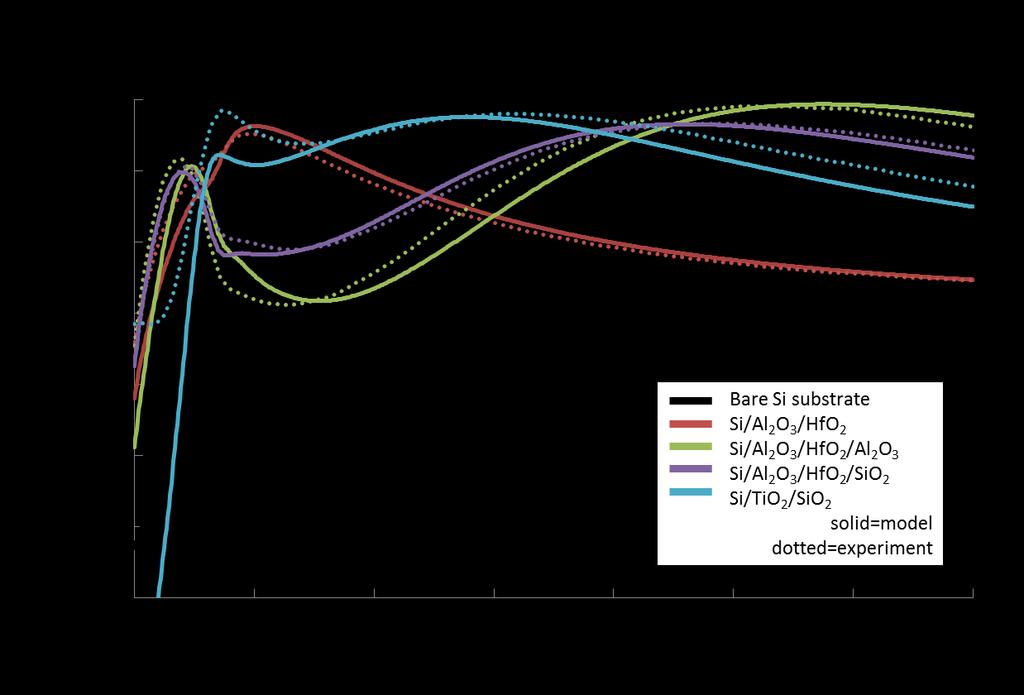
13 Preliminary QE Results on AR Coated (5-Layer), Delta Doped EMCCD More measurements required to obtain absolute QE Location of the peak matches the model!


14 ALD AR coatings, using CCD97 New ALD system greatly improves multilayer throughput Shadow mask CCD97, bonded, thinned, delta doped

15 CCD201, bonded and thinned
")

16 Far UV Rocket CHESS (sounding rocket, PI:Kevin France, Matt Beasley *CU) Collaboration with Paul Scowen, Todd Veach*, Alex Miller, ASU FUV, 3.5kx3.5k ( nm) delivered to CHESS


17 Delta-doped, AR coated fully depleted 2kx2k STA devices for WaSP guide and focus CCDs ( nm) WaSP for Palomar WaSP Photographs of an STA 3600 imager diced from a delta doped 200 micron wafer. It has been flattened against AlN and mounted in a AlN frame prior to wire bonding to flex. New packaging to accommodate WaSP requirements are under development
18


 Blue: neutral gas (dominant ion)")
19 Reflective Coatings for Astrophysics & Planetary Applications FUSE PI: Kevin France CU - CASA PI: W. Moos Johns Hopkins Reflective coatings determine the mission architecture for any UV mission (FUSE, HST/COS, etc.) FUV has a significant number of spectral lines that are of great interest to astronomers Purple: neutral gas (trace species) Blue: neutral gas (dominant ion) Green: warm, (intermediate ionization) plasma Red: highly ionized plasma Credit: T.A. Rector and B.A. Wolpa, NOAO, AURA, and NSF.
20 Benefits to Improved Mirror Coatings Aluminum mirrors require protective coatings (i.e. LiF or thick MgF 2 ) to prevent oxidation which would otherwise destroy reflectivity in the FUV Coatings also important in optical wavelengths as they affect polarization By using very thin, but high quality, MgF 2, both issues can be addressed simultaneously. Very thin coatings minimize impact on polarization of incident light Thin films of MgF 2 (1-2 nm) enable higher reflectivity (due to lower absorption losses) than LiF or thick MgF 2 Collaboration with K. France, M. Beasley* (CU) F. Greer* ( JPL) FUSE FUSE w/ improved coatings Size ~6 m ~3 m
21 XPS Characterization of ALD MgF 2 Evaporated MgF 2 ALD MgF 2 Binding Energy (ev) Binding Energy (ev) ALD MgF 2 yields similar film stoichiometry to a thermally evaporated film, but with higher resistance to oxidation after air exposure.

22 ALD MgF 2 - Performance Took simplified approach to mirror coating problem initially to look at just the performance of ALD MgF 2 itself No complications of ALD Al nucleation and cross-contamination of the films in same chamber Ellipsometry data satisfactory down to 190 nm ALD MgF 2 is amorphous as deposited at 250 C. Surprising, but extremely good result for application as protective layer TEM Prep Layers ALD MgF 2 TEM Prep Layers ALD MgF 2 Evaporated Aluminum Evaporated Aluminum
 3 Mpxl CMOS, low noise, 150 frames/")

23 Breakthrough Results in Deep UV with Alacron/Fastvision PI: Michael Hoenk. Superlattice-doped, new design, Hoenk (US patent) 3 Mpxl CMOS, low noise, 150 frames/ second, 8 wafers. Demonstrated unprecedented stability. 500x saturation exposure to Excimer laser (2 billion high energy pulses of the laser hitting the device!!). Called a breakthrough by industry!!
24 Summary Atomic scale surface engineering through MBE and ALD enable high efficiency, stable response in detectors Wafer scale and batch detector processing enable high throughput, high yield compatible with mission delivery time scale and cost Delivery to FIREBall, CHESS, WaSP progress Optical coatings using ALD under development. Characterization of ALD MgF 2 underway
Coatings. Ion Assisted Deposition (IAD) process Advance Plasma Source (APS) plasma-ion assisted Deposition. Coatings on Optical Fibers
 process Advance Plasma Source (APS) plasma-ion assisted Deposition. Coatings on Optical Fibers") Anti-Reflection Custom Ion Assisted Deposition (IAD) process Advance Plasma Source (APS) plasma-ion assisted Deposition Anti-Reflection on Optical Fibers OptoSigma supplies a wide selection of optical
Anti-Reflection Custom Ion Assisted Deposition (IAD) process Advance Plasma Source (APS) plasma-ion assisted Deposition Anti-Reflection on Optical Fibers OptoSigma supplies a wide selection of optical
State of the art quality of a GeOx interfacial passivation layer formed on Ge(001)
") APPLICATION NOTE State of the art quality of a Ox interfacial passivation layer formed on (001) Summary A number of research efforts have been made to realize Metal-Oxide-Semiconductor Field Effect Transistors
APPLICATION NOTE State of the art quality of a Ox interfacial passivation layer formed on (001) Summary A number of research efforts have been made to realize Metal-Oxide-Semiconductor Field Effect Transistors
Lecture 5. SOI Micromachining. SOI MUMPs. SOI Micromachining. Silicon-on-Insulator Microstructures. Agenda:
 EEL6935 Advanced MEMS (Spring 2005) Instructor: Dr. Huikai Xie SOI Micromachining Agenda: SOI Micromachining SOI MUMPs Multi-level structures Lecture 5 Silicon-on-Insulator Microstructures Single-crystal
Optical Coatings. Photonics 4 Luxury Coatings , Genève. Dr. Andreas Bächli Head of Optical Coatings at RhySearch, Buchs (SG)
") Optical Coatings Photonics 4 Luxury Coatings 21.06.2017, Genève Dr. Andreas Bächli Head of Optical Coatings at RhySearch, Buchs (SG) RhySearch The Research- and Innovation Center in the Rhine Valley RhySearch
Optical Coatings Photonics 4 Luxury Coatings 21.06.2017, Genève Dr. Andreas Bächli Head of Optical Coatings at RhySearch, Buchs (SG) RhySearch The Research- and Innovation Center in the Rhine Valley RhySearch
Silicon Wafer Processing PAKAGING AND TEST
 Silicon Wafer Processing PAKAGING AND TEST Parametrical test using test structures regularly distributed in the wafer Wafer die test marking defective dies dies separation die fixing (not marked as defective)
Lecture Day 2 Deposition
 Deposition Lecture Day 2 Deposition PVD - Physical Vapor Deposition E-beam Evaporation Thermal Evaporation (wire feed vs boat) Sputtering CVD - Chemical Vapor Deposition PECVD LPCVD MVD ALD MBE Plating
Thin Films: Sputtering Systems (Jaeger Ch 6 & Ruska Ch 7,) Sputtering: gas plasma transfers atoms from target to substrate Can deposit any material
 Sputtering: gas plasma transfers atoms from target to substrate Can deposit any material") Thin Films: Sputtering Systems (Jaeger Ch 6 & Ruska Ch 7,) Sputtering: gas plasma transfers atoms from target to substrate Can deposit any material on any substrate (in principal) Start with pumping down
Thin Films: Sputtering Systems (Jaeger Ch 6 & Ruska Ch 7,) Sputtering: gas plasma transfers atoms from target to substrate Can deposit any material on any substrate (in principal) Start with pumping down
Understanding Optical Coatings For Military Applications
 Understanding Optical Coatings For Military Applications By Trey Turner, Chief Technology Officer, REO Virtually all optical components used in military applications, such as target designation, rangefinding
Schottky Tunnel Contacts for Efficient Coupling of Photovoltaics and Catalysts
 Schottky Tunnel Contacts for Efficient Coupling of Photovoltaics and Catalysts Christopher E. D. Chidsey Department of Chemistry Stanford University Collaborators: Paul C. McIntyre, Y.W. Chen, J.D. Prange,
Lecture 19 Microfabrication 4/1/03 Prof. Andy Neureuther
 EECS 40 Spring 2003 Lecture 19 Microfabrication 4/1/03 Prof. ndy Neureuther How are Integrated Circuits made? Silicon wafers Oxide formation by growth or deposition Other films Pattern transfer by lithography
3.155J / 6.152J Micro/Nano Processing Technology TAKE-HOME QUIZ FALL TERM 2005
 3.155J / 6.152J Micro/Nano Processing Technology TAKE-HOME QUIZ FALL TERM 2005 1) This is an open book, take-home quiz. You are not to consult with other class members or anyone else. You may discuss the
Transmission Mode Photocathodes Covering the Spectral Range
 Transmission Mode Photocathodes Covering the Spectral Range 6/19/2002 New Developments in Photodetection 3 rd Beaune Conference June 17-21, 2002 Arlynn Smith, Keith Passmore, Roger Sillmon, Rudy Benz ITT
2Dlayer Product Catalog
 2Dlayer Product Catalog Your idea, Our materials! We provide solutions, not just materials. Tel.: 1-919-228-9662 Email: info@2dlayer.com URL: http://2dlayer.com We accept purchase orders and all kinds
Poly-SiGe MEMS actuators for adaptive optics
 Poly-SiGe MEMS actuators for adaptive optics Blake C.-Y. Lin a,b, Tsu-Jae King a, and Richard S. Muller a,b a Department of Electrical Engineering and Computer Sciences, b Berkeley Sensor and Actuator
Plasma-Enhanced Chemical Vapor Deposition
 Plasma-Enhanced Chemical Vapor Deposition Steven Glenn July 8, 2009 Thin Films Lab 4 ABSTRACT The objective of this lab was to explore lab and the Applied Materials P5000 from a different point of view.
Metallization deposition and etching. Material mainly taken from Campbell, UCCS
 Metallization deposition and etching Material mainly taken from Campbell, UCCS Application Metallization is back-end processing Metals used are aluminum and copper Mainly involves deposition and etching,
Photonic Drying Pulsed Light as a low Temperature Sintering Process
 Photonic Drying Pulsed Light as a low Temperature Sintering Process Lou Panico Xenon Corporation W E S T E R N M I C H I G A N U N I V E R S I T Y PRESENTATION OVERVIEW What is Printed Electronics Materials
Atomic Oxygen-Resistant, Static-Dissipative, Pinhole-Free Coatings for Spacecraft
 Physical Sciences Inc. VG10-109 Atomic Oxygen-Resistant, Static-Dissipative, Pinhole-Free Coatings for Spacecraft Michelle T. Schulberg, Robert H. Krech, Frederick S. Lauten Physical Sciences Inc. Roy
EE40 Lec 22. IC Fabrication Technology. Prof. Nathan Cheung 11/19/2009
 Suggested Reading EE40 Lec 22 IC Fabrication Technology Prof. Nathan Cheung 11/19/2009 300mm Fab Tour http://www-03.ibm.com/technology/manufacturing/technology_tour_300mm_foundry.html Overview of IC Technology
PRECISION OPTICAL FILTERS BY EOSS - ENHANCED OPTICAL SPUTTERING SYSTEM. Fraunhofer
 PRECISION OPTICAL FILTERS BY EOSS - ENHANCED OPTICAL SPUTTERING SYSTEM EOSS ENHANCED OPTICAL SPUTTERING SYSTEM Fraunhofer IST, Braunschweig Contact: Dr. M. Vergöhl +49 531 2155 640 EOSS Coating System
Laser Produced Plasma for Production EUV Lithography
 TRW / Cutting Edge Optronics Laser Produced Plasma for Production EUV Lithography EUVL Source Workshop October 29, 2001 TRW/CEO Laser-Produced Plasma (LPP) EUV Source Development and Commercialization
5.8 Diaphragm Uniaxial Optical Accelerometer
 5.8 Diaphragm Uniaxial Optical Accelerometer Optical accelerometers are based on the BESOI (Bond and Etch back Silicon On Insulator) wafers, supplied by Shin-Etsu with (100) orientation, 4 diameter and
Fabrication Technology
 Fabrication Technology By B.G.Balagangadhar Department of Electronics and Communication Ghousia College of Engineering, Ramanagaram 1 OUTLINE Introduction Why Silicon The purity of Silicon Czochralski
KGC SCIENTIFIC Making of a Chip
 KGC SCIENTIFIC www.kgcscientific.com Making of a Chip FROM THE SAND TO THE PACKAGE, A DIAGRAM TO UNDERSTAND HOW CPU IS MADE? Sand CPU CHAIN ANALYSIS OF SEMICONDUCTOR Material for manufacturing process
Alternative Methods of Yttria Deposition For Semiconductor Applications. Rajan Bamola Paul Robinson
 Alternative Methods of Yttria Deposition For Semiconductor Applications Rajan Bamola Paul Robinson Origin of Productivity Losses in Etch Process Aggressive corrosive/erosive plasma used for etch Corrosion/erosion
Thermal Evaporation. Theory
 Thermal Evaporation Theory 1. Introduction Procedures for depositing films are a very important set of processes since all of the layers above the surface of the wafer must be deposited. We can classify
Fig1: Melt pool size of LAMP vs. µlamp. The LAMP process s melt pool is x the area of the LAMP s melt pool.
 Proceedings of the 4th Annual ISC Research Symposium ISCRS 2010 April 21, 2010, Rolla, Missouri LOW COST IMAGING OF MELTPOOL IN MICRO LASER AIDED MANUFACTURING PROCESS (µlamp) ABSTRACT This paper describes
IISW-2009 BSI technical challenges
 IISW-2009 BSI technical challenges Bergen. 25th June 2009 Outline BSI consumer vs BSI scientific BSI vs FSI Remaining challenges Charges collection BSI overlay challenges BSI laser annealing Thinning Process
IMP EPD End Point Detector
 IMP EPD End Point Detector An overview of the Hiden Analytical SIMS end point detector system for ion beam etch applications IMP-EPD Presentation Topics The topics covered in the presentation include:
Process steps for Field Emitter devices built on Silicon wafers And 3D Photovoltaics on Silicon wafers
 Process steps for Field Emitter devices built on Silicon wafers And 3D Photovoltaics on Silicon wafers David W. Stollberg, Ph.D., P.E. Research Engineer and Adjunct Faculty GTRI_B-1 Field Emitters GTRI_B-2
Figure 2.3 (cont., p. 60) (e) Block diagram of Pentium 4 processor with 42 million transistors (2000). [Courtesy Intel Corporation.
 (e) Block diagram of Pentium 4 processor with 42 million transistors (2000). [Courtesy Intel Corporation.") Figure 2.1 (p. 58) Basic fabrication steps in the silicon planar process: (a) oxide formation, (b) selective oxide removal, (c) deposition of dopant atoms on wafer, (d) diffusion of dopant atoms into exposed
Figure 2.1 (p. 58) Basic fabrication steps in the silicon planar process: (a) oxide formation, (b) selective oxide removal, (c) deposition of dopant atoms on wafer, (d) diffusion of dopant atoms into exposed
2006 UPDATE METROLOGY
 INTERNATIONAL TECHNOLOGY ROADMAP FOR SEMICONDUCTORS METROLOGY THE ITRS DEVED AND INTENDED FOR TECHNOLOGY ASSESSMENT ONLY AND WITHOUT REGARD TO ANY COMMERCIAL CONSIDERATIONS PERTAINING TO INDIVIDUAL PRODUCTS
LOW TEMPERATURE PHOTONIC SINTERING FOR PRINTED ELECTRONICS. Dr. Saad Ahmed XENON Corporation November 19, 2015
 LOW TEMPERATURE PHOTONIC SINTERING FOR PRINTED ELECTRONICS Dr. Saad Ahmed XENON Corporation November 19, 2015 Topics Introduction to Pulsed Light Photonic sintering for Printed Electronics R&D Tools for
Photoresist Coat, Expose and Develop Laboratory Dr. Lynn Fuller
 ROCHESTER INSTITUTE OF TECHNOLOGY MICROELECTRONIC ENGINEERING Photoresist Coat, Expose and Develop Laboratory Dr. Lynn Fuller Webpage: http://www.rit.edu/lffeee 82 Lomb Memorial Drive Rochester, NY 14623-5604
Electroless CoWP Boosts Copper Reliability, Device Performance Bill Lee, Blue29, Sunnyvale, Calif. -- 7/1/2004 Semiconductor International

Supporting Information
 Supporting Information Fast-Response, Sensitivitive and Low-Powered Chemosensors by Fusing Nanostructured Porous Thin Film and IDEs-Microheater Chip Zhengfei Dai,, Lei Xu,#,, Guotao Duan *,, Tie Li *,,
Multilayer Development for Extreme Ultraviolet and Shorter Wavelength Lithography
 Multilayer Development for Extreme Ultraviolet and Shorter Wavelength Lithography Eric Louis 1, Igor Makhotkin 1, Erwin Zoethout 1, Stephan Müllender 2 and Fred Bijkerk 1,3 1 FOM Institute for Plasma Physics
VLSI Technology. By: Ajay Kumar Gautam
 By: Ajay Kumar Gautam Introduction to VLSI Technology, Crystal Growth, Oxidation, Epitaxial Process, Diffusion Process, Ion Implantation, Lithography, Etching, Metallization, VLSI Process Integration,
Measurement of thickness of native silicon dioxide with a scanning electron microscope
 Measurement of thickness of native silicon dioxide with a scanning electron microscope V. P. Gavrilenko* a, Yu. A. Novikov b, A. V. Rakov b, P. A. Todua a a Center for Surface and Vacuum Research, 40 Novatorov
Lecture 8. Deposition of dielectrics and metal gate stacks (CVD, ALD)
") Lecture 8 Deposition of dielectrics and metal gate stacks (CVD, ALD) Thin Film Deposition Requirements Many films, made of many different materials are deposited during a standard CMS process. Gate Electrodes
Lecture 8 Deposition of dielectrics and metal gate stacks (CVD, ALD) Thin Film Deposition Requirements Many films, made of many different materials are deposited during a standard CMS process. Gate Electrodes
COMPATIBILITY OF THE ALTERNATIVE SEED LAYER (ASL) PROCESS WITH MONO- Si AND POLY-Si SUBSTRATES PATTERNED BY LASER OR WET ETCHING
 PROCESS WITH MONO- Si AND POLY-Si SUBSTRATES PATTERNED BY LASER OR WET ETCHING") COMPATIBILITY OF THE ALTERNATIVE SEED LAYER (ASL) PROCESS WITH MONO- Si AND POLY-Si SUBSTRATES PATTERNED BY LASER OR WET ETCHING Lynne Michaelson 1, Anh Viet Nguyen 2, Krystal Munoz 1, Jonathan C. Wang
COMPATIBILITY OF THE ALTERNATIVE SEED LAYER (ASL) PROCESS WITH MONO- Si AND POLY-Si SUBSTRATES PATTERNED BY LASER OR WET ETCHING Lynne Michaelson 1, Anh Viet Nguyen 2, Krystal Munoz 1, Jonathan C. Wang
Amorphous Silicon Solar Cells
 The Birnie Group solar class and website were created with much-appreciated support from the NSF CRCD Program under grants 0203504 and 0509886. Continuing Support from the McLaren Endowment is also greatly
200mm Next Generation MEMS Technology update. Florent Ducrot
 200mm Next Generation MEMS Technology update Florent Ducrot The Most Exciting Industries on Earth Semiconductor Display Solar 20,000,000x reduction in COST PER TRANSISTOR in 30 years 1 20x reduction in
Substrate surface effect on the structure of cubic BN thin films from synchrotron-based X-ray diffraction and reflection
 Substrate surface effect on the structure of cubic BN thin films from synchrotron-based X-ray diffraction and reflection X.M. Zhang, W. Wen, X.L.Li, X.T. Zhou published on Dec 2012 PHYS 570 Instructor
Section 4: Thermal Oxidation. Jaeger Chapter 3. EE143 - Ali Javey
 Section 4: Thermal Oxidation Jaeger Chapter 3 Properties of O Thermal O is amorphous. Weight Density =.0 gm/cm 3 Molecular Density =.3E molecules/cm 3 O Crystalline O [Quartz] =.65 gm/cm 3 (1) Excellent
EXCIMER LASER ANNEALING FOR LOW- TEMPERATURE POLYSILICON THIN FILM TRANSISTOR FABRICATION ON PLASTIC SUBSTRATES
 EXCIMER LASER ANNEALING FOR LOW- TEMPERATURE POLYSILICON THIN FILM TRANSISTOR FABRICATION ON PLASTIC SUBSTRATES G. Fortunato, A. Pecora, L. Maiolo, M. Cuscunà, D. Simeone, A. Minotti, and L. Mariucci CNR-IMM,
Process Flow in Cross Sections
 Process Flow in Cross Sections Process (simplified) 0. Clean wafer in nasty acids (HF, HNO 3, H 2 SO 4,...) --> wear gloves! 1. Grow 500 nm of SiO 2 (by putting the wafer in a furnace with O 2 2. Coat
ME 141B: The MEMS Class Introduction to MEMS and MEMS Design. Sumita Pennathur UCSB
 ME 141B: The MEMS Class Introduction to MEMS and MEMS Design Sumita Pennathur UCSB Outline today Introduction to thin films Oxidation Deal-grove model CVD Epitaxy Electrodeposition 10/6/10 2/45 Creating
UTILIZATION OF ATMOSPHERIC PLASMA SURFACE PREPARATION TO IMPROVE COPPER PLATING PROCESSES.
 SESSION 14 MATERIALS AND PROCESSES FOR ADVANCED PACKAGING UTILIZATION OF ATMOSPHERIC PLASMA SURFACE PREPARATION TO IMPROVE COPPER PLATING PROCESSES. Eric Schulte 1, Gilbert Lecarpentier 2 SETNA Corporation
micro resist technology
 Characteristics Processing guidelines Negative Tone Photoresist Series ma-n 2400 ma-n 2400 is a negative tone photoresist series designed for the use in micro- and nanoelectronics. The resists are available
High Power Operation of Cryogenic Yb:YAG. K. F. Wall, B. Pati, and P. F. Moulton Photonics West 2007 San Jose, CA January 23, 2007
 High Power Operation of Cryogenic Yb:YAG K. F. Wall, B. Pati, and P. F. Moulton Photonics West 2007 San Jose, CA January 23, 2007 Outline Early work on cryogenic lasers MPS laser technology Recent program
Amorphous Oxide Transistor Electrokinetic Reflective Display on Flexible Glass
 Amorphous Oxide Transistor Electrokinetic Reflective Display on Flexible Glass Devin A. Mourey, Randy L. Hoffman, Sean M. Garner *, Arliena Holm, Brad Benson, Gregg Combs, James E. Abbott, Xinghua Li*,
Lecture 12. Physical Vapor Deposition: Evaporation and Sputtering Reading: Chapter 12. ECE Dr. Alan Doolittle
 Lecture 12 Physical Vapor Deposition: Evaporation and Sputtering Reading: Chapter 12 Evaporation and Sputtering (Metalization) Evaporation For all devices, there is a need to go from semiconductor to metal.
Surface micromachining and Process flow part 1
 Surface micromachining and Process flow part 1 Identify the basic steps of a generic surface micromachining process Identify the critical requirements needed to create a MEMS using surface micromachining
Semiconductor Manufacturing Technology. IC Fabrication Process Overview
 Semiconductor Manufacturing Technology Michael Quirk & Julian Serda October 00 by Prentice Hall Chapter 9 IC Fabrication Process Overview /4 Objectives After studying the material in this chapter, you
MARORA A Plasma Selective-oxidation Apparatus for Metal-gate Devices
 Hitachi Review Vol. 57 (2008), No. 3 127 MARORA A Plasma Selective-oxidation Apparatus for Metal-gate Devices Tadashi Terasaki Masayuki Tomita Katsuhiko Yamamoto Unryu Ogawa, Dr. Eng. Yoshiki Yonamoto,
Specimen Preparation Technique for a Microstructure Analysis Using the Focused Ion Beam Process
 Specimen Preparation Technique for a Microstructure Analysis Using the Focused Ion Beam Process by Kozue Yabusaki * and Hirokazu Sasaki * In recent years the FIB technique has been widely used for specimen
Large-area laser-lift-off processing in microelectronics
 Available online at www.sciencedirect.com Physics Procedia 41 (2013 ) 241 248 Lasers in Manufacturing Conference 2013 Large-area laser-lift-off processing in microelectronics R. Delmdahl*, R. Pätzel, J.
Oxide Growth. 1. Introduction
 Oxide Growth 1. Introduction Development of high-quality silicon dioxide (SiO2) has helped to establish the dominance of silicon in the production of commercial integrated circuits. Among all the various
PROVIDER OF BREAKTHROUGH TECHNOLOGY, PROCESSES AND EQUIPMENT FOR ENGINEERED SUBSTRATE SOLUTIONS. ...
 SEMICONDUCTOR SOLAR DISPLAY OPTOELECTRONIC PROVIDER OF BREAKTHROUGH TECHNOLOGY, PROCESSES AND EQUIPMENT FOR ENGINEERED SUBSTRATE SOLUTIONS........... A Look at Silicon Genesis 1997 Founded as a fabless
Flexible functional devices at mass production level with the FLEx R2R sald platform
 Flexible functional devices at mass production level with the FLEx R2R sald platform D. Spee, W. Boonen, D. Borsa and E. Clerkx Meyer Burger (Netherlands) B.V. Meyer Burger Introduction to sald Challenges
VACUUM VIEWPORTS. Introduction... I 03 KF Viewports... I 09 I 01. VACUUM / Components & Consumables
 I VAUUM VIEWPORTS Introduction... I 03 KF Viewports... I 09 I I 01 Neyco manufactures a range of UHV viewports in F, ISO or KF flange styles including a variety of coatings to enhance performance. Materials
Nanostructured Engineered Materials With High Magneto-optic Performance For Integrated Photonics Applications
 Edith Cowan University Research Online School of Engineering Publications 28 Nanostructured Engineered Materials With High Magneto-optic Performance For Integrated Photonics Applications Mikhail Vasiliev
4 Concept of Ripple Pyrometry during Flash Lamp Annealing
 4 Concept of Ripple Pyrometry during Flash Lamp Annealing 4.1 Review on Temperature Measurement for Flash Lamp Annealing Several different efforts have been undertaken to measure temperature by contactless
Processing guidelines. Negative Tone Photoresist Series ma-n 2400
 Characteristics Processing guidelines Negative Tone Photoresist Series ma-n 2400 ma-n 2400 is a negative tone photoresist series designed for the use in micro- and nanoelectronics. The resists are available
Advances in Intense Pulsed Light Solutions For Display Manufacturing. XENON Corporation Dr. Saad Ahmed Japan IDW 2016
 Advances in Intense Pulsed Light Solutions For Display Manufacturing XENON Corporation Dr. Saad Ahmed Japan IDW 2016 Talk Outline Introduction to Pulsed Light Applications in Display UV Curing Applications
Visualization and Control of Particulate Contamination Phenomena in a Plasma Enhanced CVD Reactor
 Visualization and Control of Particulate Contamination Phenomena in a Plasma Enhanced CVD Reactor Manabu Shimada, 1 Kikuo Okuyama, 1 Yutaka Hayashi, 1 Heru Setyawan, 2 and Nobuki Kashihara 2 1 Department
Surface Analysis of Electrochromic Switchable Mirror Glass Based on Magnesium-Nickel Thin Film in Accelerated Degradation Test
 Materials Transactions, Vol. 52, No. 3 (2011) pp. 464 to 468 #2011 The Japan Institute of Metals Surface Analysis of Electrochromic Switchable Mirror Glass Based on Magnesium-Nickel Thin Film in Accelerated
High Temperature Oxygen Out-Diffusion from the Interfacial SiOx Bond Layer in Direct Silicon Bonded (DSB) Substrates
 Substrates") High Temperature Oxygen Out-Diffusion from the Interfacial SiOx Bond Layer in Direct Silicon Bonded (DSB) Substrates Jim Sullivan, Harry R. Kirk, Sien Kang, Philip J. Ong, and Francois J. Henley Silicon
High Temperature Oxygen Out-Diffusion from the Interfacial SiOx Bond Layer in Direct Silicon Bonded (DSB) Substrates Jim Sullivan, Harry R. Kirk, Sien Kang, Philip J. Ong, and Francois J. Henley Silicon
Mater. Res. Soc. Symp. Proc. Vol Materials Research Society
 Mater. Res. Soc. Symp. Proc. Vol. 940 2006 Materials Research Society 0940-P13-12 A Novel Fabrication Technique for Developing Metal Nanodroplet Arrays Christopher Edgar, Chad Johns, and M. Saif Islam
E-Beam Coating Technology for EUVL Optics
 E-Beam Coating Technology for EUVL Optics Eric Louis, Andrey Yakshin, Sebastian Oestreich, Peter Görts, Marc Kessels, Edward Maas and Fred Bijkerk Institute Rijnhuizen, Nieuwegein, The Netherlands Stephan
Method to obtain TEOS PECVD Silicon Oxide Thick Layers for Optoelectronics devices Application
 Method to obtain TEOS PECVD Silicon Oxide Thick Layers for Optoelectronics devices Application ABSTRACT D. A. P. Bulla and N. I. Morimoto Laboratório de Sistemas Integráveis da EPUSP São Paulo - S.P. -
EV Group 300mm Wafer Bonding Technology July 16, 2008
 EV Group 300mm Wafer Bonding Technology July 16, 2008 EV Group in a Nutshell st Our philosophy Our mission in serving next generation application in semiconductor technology Equipment supplier for the
The Significance of Bragg s Law in Electron Diffraction and Microscopy and Bragg s Second Law
 The Significance of Bragg s Law in Electron Diffraction and Microscopy and Bragg s Second Law Colin Humphreys University of Cambridge Bragg Symposium Adelaide 6 December 2012 Bragg s Second Law E. W.
COS Monthly Status Review. September 26, 2001 GSFC
 COS GSFC Page 1 Agenda Progress Summary Since Last Monthly Optics Development Status Instrument Performance Overview UCB FUV Detector Programmatic Status UCB FUV Detector Technical Status Schedules Descope
Excimer Laser Annealing of Hydrogen Modulation Doped a-si Film
 Materials Transactions, Vol. 48, No. 5 (27) pp. 975 to 979 #27 The Japan Institute of Metals Excimer Laser Annealing of Hydrogen Modulation Doped a-si Film Akira Heya 1, Naoto Matsuo 1, Tadashi Serikawa
Vertically aligned Ni magnetic nanowires fabricated by diblock-copolymer-directed Al thin film anodization
 Vertically aligned Ni magnetic nanowires fabricated by diblock-copolymer-directed Al thin film anodization Researcher: Kunbae (Kevin) Noh, Graduate Student, MAE Dept. and CMRR Collaborators: Leon Chen,
Development of a Multi-layer Anti-reflective Coating for Gallium Arsenide/Aluminum Gallium Arsenide Solar Cells
 ARL-TR-7349 JULY 2015 US Army Research Laboratory Development of a Multi-layer Anti-reflective Coating for Gallium Arsenide/Aluminum Gallium Arsenide Solar Cells by Kimberley A Olver Approved for public
Energy Efficient Glazing Design. John Ridealgh Off-Line Coatings Technology Group Pilkington European Technology Centre
 Energy Efficient Glazing Design John Ridealgh Off-Line Coatings Technology Group Pilkington European Technology Centre 2 John Ridealgh 30th November 2009 Talk Outline Pilkington Group Limited & NSG Group
8. Epitaxy. - Extended single-crystal film formation on top of a crystalline substrate
 8. Epitaxy 1. Introduction επι(epi placed or resting upon) ταξιζ(taxis arrangement) - Extended single-crystal film formation on top of a crystalline substrate - Homoepitaxy : Film and substrate are the
From microelectronics down to nanotechnology.
 From microelectronics down to nanotechnology sami.franssila@tkk.fi Contents Lithography: scaling x- and y-dimensions MOS transistor physics Scaling oxide thickness (z-dimension) CNT transistors Conducting
R Sensor resistance (Ω) ρ Specific resistivity of bulk Silicon (Ω cm) d Diameter of measuring point (cm)
 ρ Specific resistivity of bulk Silicon (Ω cm) d Diameter of measuring point (cm)") 4 Silicon Temperature Sensors 4.1 Introduction The KTY temperature sensor developed by Infineon Technologies is based on the principle of the Spreading Resistance. The expression Spreading Resistance derives
4 Silicon Temperature Sensors 4.1 Introduction The KTY temperature sensor developed by Infineon Technologies is based on the principle of the Spreading Resistance. The expression Spreading Resistance derives
Ion-assist applications of broad-beam ion sources
 Ion-assist applications of broad-beam ion sources H.R. Kaufman a and J.M.E. Harper b a Kaufman & Robinson, Inc., 1306 Blue Spruce Dr., Fort Collins, CO 80524; b University of New Hampshire, Dept. of Physics,
Advanced Gate Stack, Source/Drain, and Channel Engineering for Si-Based CMOS 6: New Materials, Processes, and Equipment
 Advanced Gate Stack, Source/Drain, and Channel Engineering for Si-Based CMOS 6: New Materials, Processes, and Equipment Editors: E. P. Gusev Qualcomm MEMS Technologies San Jose, California, USA D-L. Kwong
Formation of and Light Emission from Si nanocrystals Embedded in Amorphous Silicon Oxides
 10.1149/1.2392914, copyright The Electrochemical Society Formation of and Light Emission from Si nanocrystals Embedded in Amorphous Silicon Oxides D. Comedi a, O. H. Y. Zalloum b, D. E. Blakie b, J. Wojcik
Isolation Technology. Dr. Lynn Fuller
 ROCHESTER INSTITUTE OF TECHNOLOGY MICROELECTRONIC ENGINEERING Isolation Technology Dr. Lynn Fuller Motorola Professor 82 Lomb Memorial Drive Rochester, NY 14623-5604 Tel (585) 475-2035 Fax (585) 475-5041
Fabrication Techniques for Thin-Film Silicon Layer Transfer
 Fabrication Techniques for Thin-Film Silicon Layer Transfer S. L. Holl a, C. A. Colinge b, S. Song b, R. Varasala b, K. Hobart c, F. Kub c a Department of Mechanical Engineering, b Department of Electrical
R&D ACTIVITIES AT ASSCP-BHEL,GURGAON IN SOLAR PV. DST-EPSRC Workshop on Solar Energy Research
 R&D ACTIVITIES AT -BHEL,GURGAON IN SOLAR PV at the DST-EPSRC Workshop on Solar Energy Research (22 nd 23 rd April, 2009) by Dr.R.K. Bhogra, Addl. General Manager & Head Email: cpdrkb@bhel.co.in Dr.A.K.
Atomic Layer Deposition(ALD)
") Atomic Layer Deposition(ALD) AlO x for diffusion barriers OLED displays http://en.wikipedia.org/wiki/atomic_layer_deposition#/media/file:ald_schematics.jpg Lam s market-leading ALTUS systems combine CVD
Atomic Layer Deposition(ALD) AlO x for diffusion barriers OLED displays http://en.wikipedia.org/wiki/atomic_layer_deposition#/media/file:ald_schematics.jpg Lam s market-leading ALTUS systems combine CVD
Radiation Damage of Polycrystalline CVD Diamond with Graphite Electrical Contacts
 Radiation Damage of Polycrystalline CVD Diamond with Graphite Electrical Contacts E. Alemanno 1,2, M. Martino 1,2, A.P. Caricato 1,2, M. Corrado 1,2, C. Pinto 1,2, S. Spagnolo 1,2, G. Chiodini 2, R. Perrino
Laser Micromachining for Industrial Applications and R&D. 3D-Micromac AG. Symposium on Smart Integrated Systems in Chemnitz. 3D-Micromac AG
 3D-Micromac AG Symposium on Smart Integrated Systems in Chemnitz 1 1 microdice - TLS-Dicing for separation of SiC 2 microprep - for high-throughput microstructure diagnostics 3 About 3D-Micromac AG 2 microdice
Real-time tablet API analysis: a comparison of a palm-size NIR spectrometer to HPLC method
 Real-time tablet API analysis: a comparison of a palm-size NIR spectrometer to HPLC method Presented by: Chris Pederson, Product Applications Engineer, JDS Uniphase Corp. Co-Authors: Nada O Brien, JDS
CMOS Manufacturing Process
 CMOS Manufacturing Process CMOS Process A Modern CMOS Process gate-oxide TiSi 2 AlCu Tungsten SiO 2 n+ p-well p-epi poly n-well p+ SiO 2 p+ Dual-Well Trench-Isolated CMOS Process Circuit Under Design V
PARAMETER EFFECTS FOR THE GROWTH OF THIN POROUS ANODIC ALUMINUM OXIDES
 10.1149/1.2794473, The Electrochemical Society PARAMETER EFFECTS FOR THE GROWTH OF THIN POROUS ANODIC ALUMINUM OXIDES S. Yim a, C. Bonhôte b, J. Lille b, and T. Wu b a Dept. of Chem. and Mat. Engr., San
Thin film silicon technology. Cosimo Gerardi 3SUN R&D Tech. Coordinator
 Thin film silicon technology Cosimo Gerardi 3SUN R&D Tech. Coordinator 1 Outline Why thin film Si? Advantages of Si thin film Si thin film vs. other thin film Hydrogenated amorphous silicon Energy gap
Solar Cells and Photosensors.
 Designing Photonic Crystals in Strongly Absorbing Material for Applications in Solar Cells and Photosensors. Minda Wagenmaker 1, Ebuka S. Arinze 2, Botong Qiu 2, Susanna M. Thon 2 1 Mechanical Engineering
A Deep Silicon RIE Primer Bosch Etching of Deep Structures in Silicon
 A Deep Silicon RIE Primer Bosch Etching of Deep Structures in Silicon April 2009 A Deep Silicon RIE Primer 1.0) Etching: Silicon does not naturally etch anisotropically in fluorine based chemistries. Si
Dallas Semicoductor DS80C320 Microcontroller
 Construction Analysis Dallas Semicoductor DS80C320 Microcontroller Report Number: SCA 9702-525 Global Semiconductor Industry the Serving Since 1964 15022 N. 75th Street Scottsdale, AZ 85260-2476 Phone:
Plastic Coated Silica/Silica (Low OH) FIBER CROSS SECTION Polyimide and Acrylate Coated. Nylon and Tefzel Coated
 FIBER CROSS SECTION Polyimide and Acrylate Coated. Nylon and Tefzel Coated") DESCRIPTION When looking for a high quality fiber with superior transmission and a numerical aperture (N.A.) of 0.22 for efficient light coupling, the is the fiber of choice. The Anhydroguide fiber is
DESCRIPTION When looking for a high quality fiber with superior transmission and a numerical aperture (N.A.) of 0.22 for efficient light coupling, the is the fiber of choice. The Anhydroguide fiber is
MODEL 1051 TEM Mill ION MILLING. Ion milling is used on physical science. specimens to reduce thickness to electron
 MODEL 1051 TEM Mill A state-of-the-art ion milling and polishing system offering reliable, high performance specimen preparation. It is compact, precise, and consistently produces high-quality transmission