Thermo-Mechanical Reliability Assessment of TSV Die Stacks by Finite Element Analysis
|
|
|
- Beverly Kennedy
- 6 years ago
- Views:
Transcription
1 Thermo-Mechanical Reliability Assessment of TSV Die Stacks by Finite Element Analysis Dr. Roland Irsigler, emens AG Corporate Technology, CT T P HTC


2 Outline TSV SOLID µbump Stacking TSV application FEA modeling appoaches Material parameter set TSV FE/BE build-up process Impact of TSV geometry on internal die level stress Regions of critical loading Packaging related stress on TSVs Options to lower the risks Summary Packaging Page 2


 Benefits: Challenges:")

3 TSV Application: DRAM TSV-Package TSV-Interconnect Chip (UP-TV) TSV s DRAM wafer TSV-Testvehicle Power Pad gnal Pad 8,0 mm Dummy Pad Via Ø 5-10 µm 12,4 mm SOLID Interconnect TSV stack (4-fold) Benefits: Challenges: memory/volume low parasitics new technology new equipment cost, yield reliability Page 3


4 FEA modeling approaches IZM Fraunhofer Institut Zuverlässigkeit und Mikrointegration 2D via model 3D via model Global/Submodel approach Al Ti/ W O2 Coupled z DOFs Coupled x DOFs O2 Polymer W Ti/ Symmetric BC Symmetric BC rotatio symmetry periodic bounderies variation in: - via diameter & pitch - layer thickness - material set Page 4 full 3D model variation in: - via shape, dimensions - via arrays - pad geometry fixed material set include build-up process flow 3D model of complete TSV-package boundary conditions for TSV submodel are determined by the global model variation in: - # of dies/stack - package construction


5 Material Regions and Dimensions 3D FE quarter -Via model with circular via cross section Coupled z DOFs* Pad of next die top region -pad Al-pad 30 µm Dielectric layer opening 17 µm 15 µm Via Ø 10 µm Sn, 2 µm, 50 µm, 4 µm O 2, 1,5 µm bottom region, 4 µm Pad of next die Polymer, here 1 µm Ti/, 50/150 nm Al, 850 nm, Ø10 µm O 2, 100 nm *Coupled degrees of freedom of the nodes at the outside area Page 5


6 3D Global Stacked Die Model and Submodelling Submodel: single via Global model: 8 fold stack in package global-local matching Interconnect side view Top die Bottom -pad IMC 3 Sn mplified die global model Bottom die Top -pad Via region At the so-called cut boundaries the displacements, which were calculated in the global model, are extrapolated on the finer mesh of the submodel. Package warpage Page 6
7 Material Parameter Set Micro Materials Center Berlin and Chemnitz Head: Prof. B. Michel Material Constitutive law (Instantaneous-) E-Modulus [MPa] Poissons ratio CTE [1/K] Initial yield stress [MPa] Source Chip Elastic 168, Normally used for <100> O 2 - Passivation x N 4 - Passivation Elastic 72, Normally used in semiconductor fabrication Elastic Normally used in semiconductor fabrication Al-Pad Elastic-plastic 70,000 at 233 K 50,000 at 523 K W-via Elastic-plastic 210,000 at 233 K -via/pad Elastic-plastic 180,000 at 523 K 103,000 at 233 K 83,000 at 673 K Ti/ Elastic-plastic 110,000 at 233 K 90,000 at 523 K σ 0 : 210;E tan : 4000 at 233K σ 0 : 180;E tan : 5000 at 523K σ0: 3100;Etan: 6900 at 233K σ 0 : 2810;E tan : 6900 at 523K σ 0 : 410;E tan : 1090 at 233K σ 0: 350;E tan: 1090 at 553K σ 0 : 540;E tan : at 233K σ 0 : 450;E tan : 7353 at 523K CINDAS (after Nanoindentation and simulation) (after Nanoindentation and simulation updated) CINDAS WPR Backside Polymer Viscoelastic, T g =100 C 4,200 at 218 K 2,800 at 423 K < 373K > 373K Shear:a1: ; a 2 : at t 1 : 45.68; t 2 : Measured in previous project IMC 3 Sn Elastic-plastic 115, σ 0 : 400 Applied in previous projects *Microelectronics Packaging Materials Database developed at Purdue University, Center for Numerical Data Analysis and Synthesis (CINDAS) under the Sponsorship of Semiconductor Research Corporation (SRC), Version 2.32, 1999 Thin film material parameter can differ significantly from bulk material parameter They can also depend on the deposition process and the source chemistry Measurements on dedicated testsamples required Page 7
8 Initial condition Process temperature [ C] TSV build-up process Elastic-plastic conditions Al-layer deposition Process Flow I deposition hard passivation upside Process Time [s] step Adjusting deposition T Wafer/die level Visco-elastic conditions Heating up to polymer deposition Process temperature [ C] Polymer deposition Ti/ deposition upside and backside Process Flow II Resist deposition Polymer etch plating upside and backside Resist strip Ti/ etch Time [s] Process Flow III The process steps up to the starting point (initial condition) can be neglected in the FE analysis because only elastic strains occur Process steps with elastic-plastic conditions were realized as loading steps with fictive time scale. Layer is stress free at deposition temperature. Non-thermal intrinsic stress (e.g. chemical shrink) were not considered. The first time step with real process time becomes effective after the deposition of the viscoelastic polymer at the wafer bottom due to its time dependent properties. Process temperature [ C] Package level Packaging Heating up to 270 C and adding 3 Sn solder Reflow soldering and cooling Molding - cooling to RT Ti/ etch Time [s] Page 8


9 ngle step vs. TSV build-up process results 1 after one equivalent cooling step Equivalent plastic strain after an intermediate step of the processing sequence Al active elements TSV / Pad interface edge Deactivated (dead) elements Al W O 2 Max. 1.9 % Max. 3.9 % W O 2 effects of the process steps have to be modeled adequately differences in stress and strain distribution patterns as well as in their amplitudes are obvious single-step approach even fails qualitatively. Page 9
10 Schematic representation of results and tendencies Results after process flow 2 Ø 15 µm Ø 2,5 µm <1 µm 10 µm Page 10


11 Results from 2D and 3D Modeling Maximum stress values in and 10x40 via 10x20 via 10x10 via 13 via array 5x1 via array circ.tsv arrays ngle rect. TSV s Page 11


 in")

12 Regions of critical loading 2D Model Al-pad Top region O 2 W S eqv [MPa] Bottom region Top region, Al Pad Al-pad W O 2 3D Model Al-pad pad O 2 Polym. Al-pad Ε pl,eqv pad Regions of stress concentrations (Indicator: v.mises stress and equiv. plastic strain) in the via structure independent of the via shape, dimension, and the level of modeling Page 12
13 FE modeling procedure to include process flow 3 ( packaging ) Create submodel (TSV) Calculation Sequential building of the TSV structure up to molding temperature 180 C Deposition temperature is stress free (reference) temperature Delete boundary conditions set for build-up Save submodel Write cut boundary nodes Create global model (package) Calculation Molding 180 C to RT Execute cut boundary interpolation for molding step Set cut boundary DOF specifications for molding-step Calculation Molding 180 C to RT Page 13
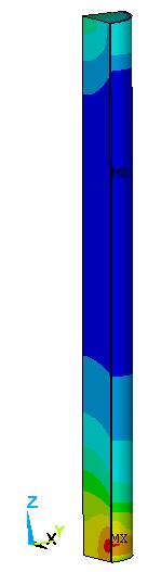
14 Via loading depending on the number of -chips in the stack Z displacements [µm] of the global model Page 14


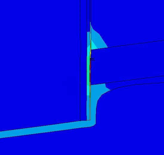
15 Results after process flow 3 ( packaging ) Top region Bottom region The via is located at the edge of a 4fold stack in package in the 2nd die from bottom of. -Pad pad O 2 ε pl,eqv Max. stress moved to outer edge of pad Polym. WPR-Pad Factor 6 higher than die level stress! Displacement scaling: 3x tilt and shear! 1% higher New quality and quantity of stress loading for the via structure after the inclusion of soldering and molding in the sequence of the build-up process Page 15
![Results after process flow 3 ( packaging ) -via filling Top region S z [MPa] ε pleqv Bottom region Plastic](/docs-images/77/75093795/images/16-0.jpg "straining is induced at the via bottom region, which accumulates during thermal cycling fatigue risk Page")
16 Results after process flow 3 ( packaging ) -via filling Top region S z [MPa] ε pleqv Bottom region Plastic straining is induced at the via bottom region, which accumulates during thermal cycling fatigue risk Page 16
17 Impact of bottom isolation layer material substitution Temperature Cycle: 125 C -55 C van-mises Stress [MPa] O2 Stress in Via Passivation Plastic Strain in the Via Initial Design PI Plastic Strain per Thermal Cylce [%] Young's Modulus of Bottom Insulator Film [GPa] 0.0 A more rigid bottom isolation layer can lower stresses and strains in the TSV bottom region Page 17
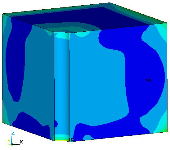
18 Impact of underfiller between dies Package without underfilling S eqv [MPa] Package with underfilling S eqv [MPa] S z [MPa] S eqv [MPa] S z [MPa] S eqv [MPa] Page 18
19 Summary General: TSV process temperature sequence has to be modeled adequately to identify critical regions and stress levels. Thin film material parameter needs to be determined properly measurements Die level: No clear failure risk for all simulated variants of via shapes found. Circuar vias and via arrays show less stress in than single, rectanular vias Local stress concentrations are /O2/Al at the top region and /O2/Polymer at the bottom region. Package level: No clear failure risk at via top region identified Clear failure risk on via bottom region due to the low stiffness of the polymer layer. Use of rigid bottom isolation layer or underfill significantly reduces stress at the via Page 19
20 Contact Dr. Roland Irsigler emens AG, CT T P HTC, Erlangen roland.irsigler@siemens.com Dr. Rainer Dudek Fraunhofer ENAS, Micro Materials Center Berlin and Chemnitz rainer.dudek@enas.fraunhofer.de Dr. Sven Rzepka Fraunhofer ENAS, Micro Materials Center Berlin and Chemnitz Sven.Rzepka@ENAS.Fraunhofer.de Thermo-Mechanical Reliability Assessment for 3D Through- Stacking, R. Dudek et al. EuromE 2009, Delft, April 2009 Virtual Prototyping in Microelectronics and Packaging, S. Rzepka et al., 33th International Conference and Exhibition IMAPS Poland 2009, September 2009 Page 20
Effects of Design, Structure and Material on Thermal-Mechanical Reliability of Large Array Wafer Level Packages
 Effects of Design, Structure and Material on Thermal-Mechanical Reliability of Large Array Wafer Level Packages Bhavesh Varia 1, Xuejun Fan 1, 2, Qiang Han 2 1 Department of Mechanical Engineering Lamar
Thermo-Mechanical FEM Analysis of Lead Free and Lead Containing Solder for Flip Chip Applications
 Thermo-Mechanical FEM Analysis of Lead Free and Lead Containing Solder for Flip Chip Applications M. Gonzalez 1, B. Vandevelde 1, Jan Vanfleteren 2 and D. Manessis 3 1 IMEC, Kapeldreef 75, 3001, Leuven,
Cu Pillar Interconnect and Chip-Package-Interaction (CPI) for Advanced Cu Low K chip
 for Advanced Cu Low K chip") EPRC 12 Project Proposal Cu Pillar Interconnect and Chip-Package-Interaction (CPI) for Advanced Cu Low K chip 15 th Aug 2012 Page 1 Introduction: Motivation / Challenge Silicon device with ultra low k
EPRC 12 Project Proposal Cu Pillar Interconnect and Chip-Package-Interaction (CPI) for Advanced Cu Low K chip 15 th Aug 2012 Page 1 Introduction: Motivation / Challenge Silicon device with ultra low k
Experience in Applying Finite Element Analysis for Advanced Probe Card Design and Study. Krzysztof Dabrowiecki Jörg Behr
 Experience in Applying Finite Element Analysis for Advanced Probe Card Design and Study Krzysztof Dabrowiecki Jörg Behr Overview A little bit of history in applying finite element analysis for probe card
Micro-tube insertion into aluminum pads: Simulation and experimental validations
 Micro-tube insertion into aluminum pads: Simulation and experimental validations A. Bedoin, B. Goubault, F. Marion, M. Volpert, F. Berger, A. Gueugnot, H. Ribot CEA, LETI, Minatec Campus 17, rue des Martyrs
Jeong et al.: Effect of the Formation of the Intermetallic Compounds (1/7)
") Jeong et al.: Effect of the Formation of the Intermetallic Compounds (1/7) Effect of the Formation of the Intermetallic Compounds between a Tin Bump and an Electroplated Copper Thin Film on both the Mechanical
Jeong et al.: Effect of the Formation of the Intermetallic Compounds (1/7) Effect of the Formation of the Intermetallic Compounds between a Tin Bump and an Electroplated Copper Thin Film on both the Mechanical
Reliability Evaluation of CIF (chip-in-flex) and COF (chip-on-flex) packages
 and COF (chip-on-flex) packages") Reliability Evaluation of CIF (chip-in-flex) and COF (chip-on-flex) packages Jae-Won Jang* a, Kyoung-Lim Suk b, Kyung-Wook Paik b, and Soon-Bok Lee a a Dept. of Mechanical Engineering, KAIST, 335 Gwahangno
Reliability Evaluation of CIF (chip-in-flex) and COF (chip-on-flex) packages Jae-Won Jang* a, Kyoung-Lim Suk b, Kyung-Wook Paik b, and Soon-Bok Lee a a Dept. of Mechanical Engineering, KAIST, 335 Gwahangno
Recent Advances in Die Attach Film
 Recent Advances in Die Attach Film Frederick Lo, Maurice Leblon, Richard Amigh, and Kevin Chung. AI Technology, Inc. 70 Washington Road, Princeton Junction, NJ 08550 www.aitechnology.com Abstract: The
Manufacturing and Reliability Modelling
 Manufacturing and Reliability Modelling Silicon Chip C Bailey University of Greenwich London, England Printed Circuit Board Airflow Temperature Stress at end of Reflow Stress Product Performance in-service
System Level Effects on Solder Joint Reliability
 System Level Effects on Solder Joint Reliability Maxim Serebreni 2004 2010 Outline Thermo-mechanical Fatigue of solder interconnects Shear and tensile effects on Solder Fatigue Effect of Glass Style on
Field Condition Reliability Assessment for SnPb and SnAgCu Solder Joints in Power Cycling Including Mini Cycles
 Field Condition Reliability Assessment for SnPb and SnAgCu Solder Joints in Power Cycling Including Mini Cycles Min Pei 1, Xuejun Fan 2 and Pardeep K. Bhatti 2 1 Georgia Tech, 801 Ferst Dr. NW, Atlanta,
NANOINDENTATION OF SILICON CARBIDE WAFER COATINGS
 NANOINDENTATION OF SILICON CARBIDE WAFER COATINGS Prepared by Jesse Angle 6 Morgan, Ste156, Irvine CA 9618 P: 949.461.99 F: 949.461.93 nanovea.com Today's standard for tomorrow's materials. 010 NANOVEA
Power Electronics Packaging Solutions for Device Junction Temperature over 220 o C
 EPRC 12 Project Proposal Power Electronics Packaging Solutions for Device Junction Temperature over 220 o C 15 th August 2012 Page 1 Motivation Increased requirements of high power semiconductor device
Avatrel Stress Buffer Coatings: Low Stress Passivation and Redistribution Applications
 Avatrel Stress Buffer Coatings: Low Stress Passivation and Redistribution Applications Ed Elce, Chris Apanius, Jeff Krotine, Jim Sperk, Andrew Bell, Rob Shick* Sue Bidstrup-Allen, Paul Kohl Takashi Hirano,
Simulation of Embedded Components in PCB Environment and Verification of Board Reliability
 Simulation of Embedded Components in PCB Environment and Verification of Board Reliability J. Stahr, M. Morianz AT&S Leoben, Austria M. Brizoux, A. Grivon, W. Maia Thales Global Services Meudon-la-Forêt,
3D Package Technologies Review with Gap Analysis for Mobile Application Requirements. Apr 22, 2014 STATS ChipPAC Japan
 3D Package Technologies Review with Gap Analysis for Mobile Application Requirements Apr 22, 2014 STATS ChipPAC Japan T.Nishio Contents Package trends and roadmap update Advanced technology update Fine
Ultra Fine Pitch Bumping Using e-ni/au and Sn Lift-Off Processes
 Ultra Fine Pitch Bumping Using e-ni/au and Sn Lift-Off Processes Andrew Strandjord, Thorsten Teutsch, and Jing Li Pac Tech USA Packaging Technologies, Inc. Santa Clara, CA USA 95050 Thomas Oppert, and
IMPACT OF LEAD-FREE COMPONENTS AND TECHNOLOGY SCALING FOR HIGH RELIABILITY APPLICATIONS
 IMPACT OF LEAD-FREE COMPONENTS AND TECHNOLOGY SCALING FOR HIGH RELIABILITY APPLICATIONS Chris Bailey, Ph.D. University of Greenwich London, United Kingdom c.bailey@gre.ac.uk ABSTRACT Semiconductor technology
PARASITIC EFFECTS REDUCTION FOR WAFER-LEVEL PACKAGING OF RF-MEMS
 Stresa, Italy, 26-28 April 2006 J. Iannacci 1,2, J. Tian 1, S.M. Sinaga 1, R. Gaddi 2, A. Gnudi 2, and M. Bartek 1 1) HiTeC-DIMES, Delft University of Technology, Mekelweg 4, 2628 CD Delft, the Netherlands
Design, Analysis and Manufacturing of a Re-Entry Capsule made by Inflatable Structures
 Design, Analysis and Manufacturing of a Re-Entry Capsule made by Inflatable Structures E. Carrera a, L. Montefiore a, E. Beruto b, G. Augello b, M. Adami c, A. Hromadkova c, E. Gabellini d a Aerospace
178 IEEE TRANSACTIONS ON COMPONENTS, PACKAGING AND MANUFACTURING TECHNOLOGY, VOL. 7, NO. 2, FEBRUARY 2017
 178 IEEE TRANSACTIONS ON COMPONENTS, PACKAGING AND MANUFACTURING TECHNOLOGY, VOL. 7, NO. 2, FEBRUARY 2017 Experimental and Theoretical Assessment of Thin Glass Substrate for Low Warpage Scott McCann, Vanessa
A Review of Suitability for PWHT Exemption Requirements in the Aspect of Residual Stresses and Microstructures
 Transactions, SMiRT-23 Division IX, Paper ID 612 (inc. assigned division number from I to X) A Review of Suitability for PWHT Exemption Requirements in the Aspect of Residual Stresses and Microstructures
Parametric Design and Reliability Analysis of Wire Interconnect Technology Wafer Level Packaging
 Y. T. Lin Graduate Assistant C. T. Peng Graduate Assistant K. N. Chiang Associate Professor e-mail: Knchiang@pme.nthu.edu.tw Dept. of Power Mechanical Engineering, National Tsing Hua University, HsinChu
Micro-Electro-Mechanical Systems (MEMS) Fabrication. Special Process Modules for MEMS. Principle of Sensing and Actuation
 Fabrication. Special Process Modules for MEMS. Principle of Sensing and Actuation") Micro-Electro-Mechanical Systems (MEMS) Fabrication Fabrication Considerations Stress-Strain, Thin-film Stress, Stiction Special Process Modules for MEMS Bonding, Cavity Sealing, Deep RIE, Spatial forming
Micro-Electro-Mechanical Systems (MEMS) Fabrication Fabrication Considerations Stress-Strain, Thin-film Stress, Stiction Special Process Modules for MEMS Bonding, Cavity Sealing, Deep RIE, Spatial forming
Materials Characterization for Stress Management
 Materials Characterization for Stress Management Ehrenfried Zschech, Fraunhofer IZFP Dresden, Germany Workshop on Stress Management for 3D ICs using TSVs San Francisco/CA, July 13, 2010 Outline Stress
An Innovative High Throughput Thermal Compression Bonding Process
 An Innovative High Throughput Thermal Compression Bonding Process Li Ming 2 September 2015 Outline Introduction Throughput improved TCB Process Liquid Phase Contact (LPC) bonding Flux-LPC-TCB under inert
Chips Face-up Panelization Approach For Fan-out Packaging
 Chips Face-up Panelization Approach For Fan-out Packaging Oct. 15, 2015 B. Rogers, D. Sanchez, C. Bishop, C. Sandstrom, C. Scanlan, TOlson T. REV A Background on FOWLP Fan-Out Wafer Level Packaging o Chips
FEM STRESS CONCENTRATION FACTORS FOR FILLET WELDED CHS-PLATE T-JOINT
 Engineering Review Vol. 32, Issue 3, 147-155, 2012. 147 FEM STRESS CONCENTRATION FACTORS FOR FILLET WELDED CHS-PLATE T-JOINT S. * G. Turkalj Department of Engineering Mechanics, Faculty of Engineering,
Evaluation of Cu Pillar Chemistries
 Presented at 2016 IMAPS Device Packaging Evaluation of Cu Pillar Chemistries imaps Device Packaging Conference Spring 2016 Matthew Thorseth, Mark Scalisi, Inho Lee, Sang-Min Park, Yil-Hak Lee, Jonathan
TSV CHIP STACKING MEETS PRODUCTIVITY
 TSV CHIP STACKING MEETS PRODUCTIVITY EUROPEAN 3D TSV SUMMIT 22-23.1.2013 GRENOBLE HANNES KOSTNER DIRECTOR R&D BESI AUSTRIA OVERVIEW Flip Chip Packaging Evolution The Simple World of C4 New Flip Chip Demands
Reliability Challenges for 3D Interconnects:
 Reliability Challenges for 3D Interconnects: A material and design perspective Paul S. Ho Suk-Kyu Ryu, Kuan H. (Gary) Lu, Qiu Zhao, Jay Im and Rui Huang The University of Texas at Austin 3D Sematech Workshop,
3D FRACTURE MECHANICS ANALYSIS OF UNDERFILL DELAMINATION FOR FLIP CHIP PACKAGES
 3D FRACTURE MECHANICS ANALYSIS OF UNDERFILL DELAMINATION FOR FLIP CHIP PACKAGES Zhen Zhang, Charlie J Zhai, and Raj N Master Advanced Micro Devices, Inc. 1050 E. Arques Ave., Sunnyvale, CA 94085, USA Phone:
Vibration Analysis of Propeller Shaft Using FEM.
 Vibration Analysis of Propeller Shaft Using FEM. 1 Akshay G. Khande, 2 Shreyash A. Sable, 3 Vaibhav R. Bidwai, 4 Chandrasekhar B. Aru, 5 Brahmanand S.Jadhav 12345 Mechanical Engineering Department, Babasahebh
Challenges for Embedded Device Technologies for Package Level Integration
 Challenges for Embedded Device Technologies for Package Level Integration Kevin Cannon, Steve Riches Tribus-D Ltd Guangbin Dou, Andrew Holmes Imperial College London Embedded Die Technology IMAPS-UK/NMI
Copyright 2009 Year IEEE. Reprinted from 2009 Electronic Components and Technology Conference. Such permission of the IEEE does not in any way imply
 Copyright 2009 Year IEEE. Reprinted from 2009 Electronic Components and Technology Conference. Such permission of the IEEE does not in any way imply IEEE endorsement of any of Institute of Microelectronics
Behaviors of QFN Packages on a Leadframe Strip
 Behaviors of QFN Packages on a Leadframe Strip Eric Ouyang, Billy Ahn, Seng Guan Chow, Anonuevo Dexter, SeonMo Gu, YongHyuk Jeong, JaeMyong Kim STATS ChipPAC Inc 46429 Landing Parkway, Fremont, CA 94538,
Thermal Management of Die Stacking Architecture That Includes Memory and Logic Processor
 Thermal Management of Die Stacking Architecture That Includes Memory and Logic Processor Bhavani P. Dewan-Sandur, Abhijit Kaisare and Dereje Agonafer The University of Texas at Arlington, Box 19018, TX
INTEGRATED FINITE ELEMENT ENVIRONMENT FOR COMPOSITE PROCESS SIMULATION
 INTEGRATED FINITE ELEMENT ENVIRONMENT FOR COMPOSITE PROCESS SIMULATION Tomasz Garstka, Garry Cole, David Irving, Paul Lyons Finite Element Analysis Limited, Forge House, 66 High Street, Kingston upon Thames,
Topography and Deformation Measurement and FE Modeling Applied to substrate-mounted large area wafer-level packages (including stacked dice and TSVs)
") Topography and Deformation Measurement and FE Modeling Applied to substrate-mounted large area wafer-level packages (including stacked dice and TSVs) M. Hertl Insidix, 24 rue du Drac, 38180 Grenoble/Seyssins,
Topography and Deformation Measurement and FE Modeling Applied to substrate-mounted large area wafer-level packages (including stacked dice and TSVs) M. Hertl Insidix, 24 rue du Drac, 38180 Grenoble/Seyssins,
curamik CERAMIC SUBSTRATES AMB technology Design Rules Version #04 (09/2015)
") curamik CERAMIC SUBSTRATES AMB technology Design Rules Version #04 (09/2015) Content 1. Geometric properties 1.01. Available ceramic types / thicknesses... 03 1.02. thicknesses (standard)... 03 3. Quality
curamik CERAMIC SUBSTRATES AMB technology Design Rules Version #04 (09/2015) Content 1. Geometric properties 1.01. Available ceramic types / thicknesses... 03 1.02. thicknesses (standard)... 03 3. Quality
IMPLEMENTATION OF A FULLY MOLDED FAN-OUT PACKAGING TECHNOLOGY
 IMPLEMENTATION OF A FULLY MOLDED FAN-OUT PACKAGING TECHNOLOGY B. Rogers, C. Scanlan, and T. Olson Deca Technologies, Inc. Tempe, AZ USA boyd.rogers@decatechnologies.com ABSTRACT Fan-Out Wafer-Level Packaging
An Advanced Reliability Improvement and Failure Analysis Approach to Thermal Stress Issues in IC Packages
 An Advanced Reliability Improvement and Failure Analysis Approach to Thermal Stress Issues in IC Packages Michael Hertl 1, Diane Weidmann 1, and Alex Ngai 2 1 Insidix, 24 rue du Drac, F-38180 Grenoble/Seyssins,
Available online at ScienceDirect. Procedia Engineering 79 (2014 )
") Available online at www.sciencedirect.com ScienceDirect Procedia Engineering 79 (2014 ) 333 338 37th National Conference on Theoretical and Applied Mechanics (37th NCTAM 2013) & The 1st International Conference
Available online at www.sciencedirect.com ScienceDirect Procedia Engineering 79 (2014 ) 333 338 37th National Conference on Theoretical and Applied Mechanics (37th NCTAM 2013) & The 1st International Conference
Reduced Ductility due to Local Variation in Material Properties for 3D-printed Components
 Reduced Ductility due to Local Variation in Material Properties for 3D-printed Components T. Tryland SINTEF Raufoss Manufacturing, Raufoss, Norway 1 Background It is often useful to have a physical model
Package Design Optimization and Materials Selection for Stack Die BGA Package
 Package Design Optimization and Materials Selection for Stack Die BGA Package Rahul Kapoor, Lim Beng Kuan, Liu Hao United Test & Assembly Center Ltd (UTAC) 5 Serangoon North Ave 5, Singapore 554916 Email:
Flip-Chip Process Improvements for Low Warpage
 Flip-Chip Process Improvements for Low Warpage Robert L. Hubbard Lambda Technologies, Inc. Morrisville, NC, USA bhubbard@microcure.com Pierino Zappella*, Pukun Zhu Henkel Corporation Irvine, CA, USA Abstract
Novel Materials and Activities for Next Generation Package. Hitachi Chemical., Co.Ltd. Packaging Solution Center Hiroaki Miyajima
 Novel Materials and Activities for Next Generation Package Hitachi Chemical., Co.Ltd. Packaging Solution Center Hiroaki Miyajima 1. Activities of Packaging Solution Center 2. Novel Materials for Next Gen.
Study on Mixed Mode Crack-tip Plastic Zones in CTS Specimen
 Proceedings of the World Congress on Engineering Vol II WCE, July -,, London, U.K. Study on Mixed Mode Crack-tip Plastic Zones in Specimen C. M. Sharanaprabhu, S. K. Kudari Member, IAENG Abstract The studies
EFFECT OF LOCAL WALL THINNING ON FRACTURE BEHAVIOR OF STRAIGHT PIPE
 ECF EFFECT OF LOCAL WALL THINNING ON FRACTURE BEHAVIOR OF STRAIGHT PIPE Masato Ono, Ki-Woo Nam*, Koji Takahashi, Kotoji Ando Department of Safety & Energy Engineering, Yokohama National University 79-
A Solder Joint Reliability Model for the Philips Lumileds LUXEON Rebel LED Carrier Using Physics of Failure Methodology
 A Solder Joint Reliability Model for the Philips Lumileds LUXEON Rebel LED Carrier Using Physics of Failure Methodology Rudi Hechfellner 1, Michiel Kruger 1, Tewe Heemstra 2 Greg Caswell 3, Nathan Blattau
SUSS SOLUTIONS FOR LARGE FORMAT PATTERNING UV Scanning Lithography and Excimer Laser Ablation
 SUSS SOLUTIONS FOR LARGE FORMAT PATTERNING UV Scanning Lithography and Excimer Laser Ablation Kevin Yang, Habib Hichri, Ralph Zoberbier SÜSS MicroTec Photonic Systems Inc. June 18, 2015 MARKET DRIVER Mobile
Board Level Reliability Improvement in ewlb (Embedded Wafer Level BGA) Packages
 Packages") Board Level Reliability Improvement in ewlb (Embedded Wafer Level BGA) Packages by Seng Guan Chow, Yaojian Lin, Bernard Adams * and Seung Wook Yoon** STATS ChipPAC Ltd. 5 Yishun Street 23, Singapore 768442
Board Level Reliability Improvement in ewlb (Embedded Wafer Level BGA) Packages by Seng Guan Chow, Yaojian Lin, Bernard Adams * and Seung Wook Yoon** STATS ChipPAC Ltd. 5 Yishun Street 23, Singapore 768442
Reliability of Interconnects in LED Lighting Assemblies Utilizing Metal Clad Printed Circuit Boards Stefano Sciolè BDM I.M.S.
 Reliability of Interconnects in LED Lighting Assemblies Utilizing Metal Clad Printed Circuit Boards Stefano Sciolè BDM I.M.S. Henkel Electronic Materials Agenda 1. Introduction 2. Motivation 3. Interconnect
Compressive strength of double-bottom under alternate hold loading condition
 Progress in the Analysis and Design of Marine Structures Guedes Soares & Garbatov (Eds) 017 Taylor & Francis Group, London, ISBN 978-1-138-06907-7 Compressive strength of double-bottom under alternate
Design under high windload
 Structural Glazing: Design under high windload Pierre Descamps Dow Corning Corporation, Belgium Jon Kimberlain Dow Corning Corporation, Midland (United States) Jayrold Bautista Dow Corning Corporation,
Investigation on Flip Chip Solder Joint Fatigue With Cure-Dependent Underfill Properties
 388 IEEE TRANSACTIONS ON COMPONENTS AND PACKAGING TECHNOLOGIES, VOL. 26, NO. 2, JUNE 2003 Investigation on Flip Chip Solder Joint Fatigue With Cure-Dependent Underfill Properties D. G. Yang, G. Q. Zhang,
Silicon Wafer Processing PAKAGING AND TEST
 Silicon Wafer Processing PAKAGING AND TEST Parametrical test using test structures regularly distributed in the wafer Wafer die test marking defective dies dies separation die fixing (not marked as defective)
Wire-bonds Durability in High-temperature Applications M. Klíma, B. Psota, I. Szendiuch
 Ročník 2013 Číslo V Wire-bonds Durability in High-temperature Applications M. Klíma, B. Psota, I. Szendiuch Department of Microelectronics, Faculty of Electrical Engineering and Communication, Brno University
White Paper Quality and Reliability Challenges for Package on Package. By Craig Hillman and Randy Kong
 White Paper Quality and Reliability Challenges for Package on Package By Craig Hillman and Randy Kong Background Semiconductor technology advances have been fulfilling Moore s law for many decades. However,
Lead-Free Solder Bump Technologies for Flip-Chip Packaging Applications
 Lead-Free Solder Bump Technologies for Flip-Chip Packaging Applications Zaheed S. Karim 1 and Jim Martin 2 1 Advanced Interconnect Technology Ltd. 1901 Sunley Centre, 9 Wing Yin Street, Tsuen Wan, Hong
PCB Technologies for LED Applications Application note
 PCB Technologies for LED Applications Application note Abstract This application note provides a general survey of the various available Printed Circuit Board (PCB) technologies for use in LED applications.
Flip-Chip Process Improvements for Low Warpage
 Flip-Chip Process Improvements for Low Warpage Robert L. Hubbard Lambda Technologies, Inc. Morrisville, NC, USA bhubbard@microcure.com Pierino Zappella*, Pukun Zhu Henkel Corporation Irvine, CA, USA Abstract
"ewlb Technology: Advanced Semiconductor Packaging Solutions"
 "ewlb Technology: Advanced Semiconductor Packaging Solutions" by Sharma Gaurav@, S.W. Yoon, Yap Yok Mian, Shanmugam Karthik, Yaojian Lin, Pandi C. Marimuthu and Yeong J. Lee* STATS ChipPAC Ltd. 5 Yishun
3D Finite Element Modeling and Analysis of Micromechanical Sensors
 Abstract 3D Finite Element Modeling and Analysis of Micromechanical Sensors Alexey I. Borovkov, Eugeny V. Pereyaslavets Computational Mechanics Laboratory, St. Petersburg State Technical University, Russia
RF System in Packages using Integrated Passive Devices
 RF System in Packages using Integrated Passive Devices by Kai Liu, YongTaek Lee, HyunTai Kim, Gwang Kim, and Billy Ahn STATS ChipPAC 1711 W. Greentree Drive, Suite #117, Tempe, AZ 85284, USA Tel: 480-222-1722
Compressive strength of double-bottom under alternate hold loading condition
 Compressive strength of double-bottom under alternate hold loading condition J.M. Gordo CENTEC, IST, University of Lisbon, Portugal ABSTRACT: The alternate bending of the bottom structure of a ship as
FABRICATION AND RELIABILITY OF ULTRA-FINE RDL STRUCTURES IN ADVANCED PACKAGING BY EXCIMER LASER ABLATION
 FABRICATION AND RELIABILITY OF ULTRA-FINE RDL STRUCTURES IN ADVANCED PACKAGING BY EXCIMER LASER ABLATION NCCAVS Joint Users Group Technical Symposium San Jose, June 7 th, 2017 Markus Arendt, SÜSS MicroTec
TSV Processing and Wafer Stacking. Kathy Cook and Maggie Zoberbier, 3D Business Development
 TSV Processing and Wafer Stacking Kathy Cook and Maggie Zoberbier, 3D Business Development Outline Why 3D Integration? TSV Process Variations Lithography Process Results Stacking Technology Wafer Bonding
SEMI MEMS Tech Seminar (Sept 26, Cornaredo, Italy)
") SEMI MEMS Tech Seminar (Sept 26, 2013 - Cornaredo, Italy) Opportunities of Wafer Level Embedded Technologies for MEMS Devices T. Braun ( 1 ), K.-F. Becker ( 1 ), R. Kahle ( 2 ), V. Bader ( 1 ), S. Voges
SEMI MEMS Tech Seminar (Sept 26, 2013 - Cornaredo, Italy) Opportunities of Wafer Level Embedded Technologies for MEMS Devices T. Braun ( 1 ), K.-F. Becker ( 1 ), R. Kahle ( 2 ), V. Bader ( 1 ), S. Voges
Modelling Embedded Die Systems
 Modelling Embedded Die Systems Stoyan Stoyanov and Chris Bailey Computational Mechanics and Reliability Group (CMRG) University of Greenwich, London, UK 22 September 2016 IMAPS/NMI Conference on EDT Content
THIN IMMERSION TIN USING ORGANIC METALS
 THIN IMMERSION TIN USING ORGANIC METALS Jim Kenny, Nils Arendt, Bernhard Wessling, and Karl Wengenroth Enthone Inc., A Business of Cookson Electronics West Haven, CT, USA ABSTRACT With the international
a. 50% fine pearlite, 12.5% bainite, 37.5% martensite. 590 C for 5 seconds, 350 C for 50 seconds, cool to room temperature.
 Final Exam Wednesday, March 21, noon to 3:00 pm (160 points total) 1. TTT Diagrams A U.S. steel producer has four quench baths, used to quench plates of eutectoid steel to 700 C, 590 C, 350 C, and 22 C
Thermo-mechanical mechanical coupled simulation of hot forming processes considering die cooling
 Thermo-mechanical mechanical coupled simulation of hot forming processes considering die cooling M. Medricky 1, R. Struck 1, C. Sunderkötter 1, D. Lorenz 2, P. Olle 3, B.-A. Behrens 3 1 Volkswagen Group
Simulation of Residual Deformation from a Forming and Welding Process using LS-DYNA
 13 th International LS-DYNA Users Conference Session: Simulation Simulation of Residual Deformation from a Forming and Welding Process using LS-DYNA Mikael Schill 1, Eva-Lis Odenberger 2 1 DYNAmore Nordic
TSV Interposer Process Flow with IME 300mm Facilities
 TSV Interposer Process Flow with IME 300mm Facilities Property of Institute of Microelectronics (IME)-Singapore August 17, 2012 Outline 1. TSV interposer (TSI) cross sectional schematic TSI with BEOL,
AN Handling and processing of sawn wafers on UV dicing tape. Document information. Sawn wafers, UV dicing tape, handling and processing
 Handling and processing of sawn wafers on UV dicing tape Rev. 2.0 13 January 2009 Application note Document information Info Keywords Abstract Content Sawn wafers, UV dicing tape, handling and processing
Todd F. Shupe Associate Professor School of Renewable Natural Resources Louisiana State University AgCenter Baton Rouge, LA 70803
 FINITE ELEMENT ANALYSES OF WOOD LAMINATED COMPOSITE POLES 1 Cheng Piao Postdoctoral Research Associate USDA Forest Service Forest Products Laboratory Madison, WI 53726 Todd F. Shupe Associate Professor
FRAUNHOFER INSTITUTE FOR RELIABILITY AND MICROINTEGRATION IZM DEPARTMENT WAFER LEVEL SYSTEM INTEGRATION BERLIN
 FRAUNHOFER INSTITUTE FOR RELIABILITY AND MICROINTEGRATION IZM DEPARTMENT WAFER LEVEL SYSTEM INTEGRATION BERLIN WAFER LEVEL SYSTEM INTEGRATION ELECTRONIC PACKAGING AT FRAUNHOFER IZM The Fraunhofer Institute
STUDY OF POLYMER FLOW BEHAVIOR IN CAVITY FILLING OF ALIGNMENT STRUCTURES IN MICRO HOT EMBOSSING THESIS
 i STUDY OF POLYMER FLOW BEHAVIOR IN CAVITY FILLING OF ALIGNMENT STRUCTURES IN MICRO HOT EMBOSSING THESIS Presented to the Graduate Council of Texas State University-San Marcos in Partial Fulfillment of
FRAUNHOFER INSTITUTE FOR MACHINE TOOLS AND FORMING TECHNOLOGY IWU SIMULATION IN FORMING TECHNOLOGY
 FRAUNHOFER INSTITUTE FOR MACHINE TOOLS AND FORMING TECHNOLOGY IWU SIMULATION IN FORMING TECHNOLOGY 1 SIMULATION IN SHEET METAL FORMING Simulation is an essential part of the development chain, especially
Thin Wafers Bonding & Processing
 Thin Wafers Bonding & Processing A market perspective 2012 Why New Handling Technologies Consumer electronics is today a big driver for smaller, higher performing & lower cost device configurations. These
Study of Cracking of Thin Glass Interposers Intended for Microelectronic Packaging Substrates
 Study of Cracking of Thin Glass Interposers Intended for Microelectronic Packaging Substrates Scott R. McCann 1,2, Yoichiro Sato 3, Venkatesh Sundaram 1,4, Rao R. Tummala 1,4,5, and Suresh K. Sitaraman
A MODEL FOR RESIDUAL STRESS AND PART WARPAGE PREDICTION IN MATERIAL EXTRUSION WITH APPLICATION TO POLYPROPYLENE. Atlanta, GA 30332
 Solid Freeform Fabrication 2016: Proceedings of the 26th 27th Annual International Solid Freeform Fabrication Symposium An Additive Manufacturing Conference A MODEL FOR RESIDUAL STRESS AND PART WARPAGE
E APPENDIX. The following problems are intended for solution using finite element. Problems for Computer Solution E.1 CHAPTER 3
 E APPENDIX Problems for Computer Solution The following problems are intended for solution using finite element analysis software. In general, the problems associated with Chapters 3, 4, and 9 can be solved
NPL Manual. Modelling Creep in Toughened Epoxy Adhesives
 NPL Manual Modelling Creep in Toughened Epoxy Adhesives This Electronic Guide was produced as part of the Measurements for Materials System Programme on Design for Fatigue and Creep in Joined Systems Introduction
FINITE ELEMENT MODELING TECHNIQUES OF 3D WELDED JOINTS THE STRUCTURAL HOT SPOT APPROACH
 FINITE ELEMENT MODELING TECHNIQUES OF 3D WELDED JOINTS THE STRUCTURAL HOT SPOT APPROACH Keurrie Cipriano Goes, keurrie.goes@arvinmeritor.com ArvinMeritor do Brasil Sistemas Automotivos Commercial Vehicle
System-in-Package (SiP) on Wafer Level, Enabled by Fan-Out WLP (ewlb)
 on Wafer Level, Enabled by Fan-Out WLP (ewlb)") System-in-Package (SiP) on Wafer Level, Enabled by Fan-Out WLP (ewlb) Steffen Kröhnert, José Campos, Eoin O Toole NANIUM S.A., Vila do Conde, Portugal Outline Short Company Overview NANIUM Introduction
System-in-Package (SiP) on Wafer Level, Enabled by Fan-Out WLP (ewlb) Steffen Kröhnert, José Campos, Eoin O Toole NANIUM S.A., Vila do Conde, Portugal Outline Short Company Overview NANIUM Introduction
Finite Element Analysis on the Unloading Elastic Modulus of Aluminum Foams by Unit-cell Model
 IOP Conference Series: Materials Science and Engineering PAPER OPEN ACCESS Finite Element Analysis on the Unloading Elastic Modulus of Aluminum Foams by Unit-cell Model To cite this article: F Triawan
Simulation Study on the Warpage Behavior and Board-level Temperature Cycling Reliability of PoP Potentially for High-speed Memory Packaging
 Simulation Study on the Warpage Behavior and Board-level Temperature Cycling Reliability of PoP Potentially for High-speed Memory Packaging Wei Sun, W.H. Zhu, Kriangsak Sae Le and H.B. Tan United Test
EUV Mask Image Placement Management in Writing, Registration, and Exposure Tools
 EUV Mask Image Placement Management in Writing, Registration, and Exposure Tools Eric Cotte a *, Uwe Dersch a, Christian Holfeld a, Uwe Mickan b, Holger Seitz c, Thomas Leutbecher c, and Günter Hess c
M3 Review Automated Nanoindentation
 M3 Review Automated Nanoindentation Prepared by Duanjie Li, PhD & Pierre Leroux 6 Morgan, Ste156, Irvine CA 92618 P: 949.461.9292 F: 949.461.9232 nanovea.com Today's standard for tomorrow's materials.
An example of finite element modelling of progressive collapse
 COST Action TU0601 Robustness of Structures 2nd and 3rd of March 2009 Coimbra, Portugal An example of finite element modelling of progressive collapse Leslaw KWASNIEWSKI Marian A. GIZEJOWSKI Faculty of
Key words: microprocessor integrated heat sink Electronic Packaging Material, Thermal Management, Thermal Conductivity, CTE, Lightweight
 Aluminum Silicon Carbide (AlSiC) Microprocessor Lids and Heat Sinks for Integrated Thermal Management Solutions Mark A. Occhionero, Robert A. Hay, Richard W. Adams, Kevin P. Fennessy, and Glenn Sundberg
Nonlinear Finite Element Modeling & Simulation
 Full-Scale Structural and Nonstructural Building System Performance during Earthquakes & Post-Earthquake Fire A Joint Venture between Academe, Industry and Government Nonlinear Finite Element Modeling
Study on ultimate strength of ship plates with calculated weld-induced residual stress
 Maritime Technology and Engineering Guedes Soares & Santos (Eds) 2015 Taylor & Francis Group, London, ISBN 978-1-138-02727-5 Study on ultimate strength of ship plates with calculated weld-induced residual
YIELD & TENSILE STRENGTH OF STEEL & ALUMINIUM USING MICROINDENTATION
 YIELD & TENSILE STRENGTH OF STEEL & ALUMINIUM USING MICROINDENTATION Prepared by Duanjie Li, PhD & Pierre Leroux 6 Morgan, Ste156, Irvine CA 9618 P: 949.461.99 F: 949.461.93 nanovea.com Today's standard
Effect of Encapsulation Materials on Tensile Stress during Thermo-Mechanical Cycling of Pb-Free Solder Joints
 Effect of Encapsulation Materials on Tensile Stress during Thermo-Mechanical Cycling of Pb-Free Solder Joints Maxim Serebreni, Dr. Nathan Blattau, Dr. Gilad Sharon, Dr. Craig Hillman DfR Solutions Beltsville,
Panel Discussion: Advanced Packaging
 Dr. Steve Bezuk Senior Director IC Packaging Engineering Qualcomm Technologies, Inc. Panel Discussion: Advanced Packaging PAGE 1 Technical Challenges of Packaging (Mobile Focus) Materials Die materials
Numerical study of residual stresses formation during the APS process
 Numerical study of residual stresses formation during the APS process J.Li, R. Bolot, H.Liao and C.Coddet, LERMPS-UTBM, Belfort /F The formation of residual stresses during thermal spray processes may
Simulation of welding using MSC.Marc. Paper reference number:
 Simulation of welding using MSC.Marc Paper reference number: 2001-29 Tor Morten Olsen 1, Henrik Runnemalm 1 and Daniel Berglund 1, 2 1 Volvo Aero Corporation, Trollhettan, Sweden Tor-morten.olsen@volvo.com