Failure Analysis: The Right Way
|
|
|
- Lambert Hensley
- 6 years ago
- Views:
Transcription
1 i Failure Analysis: The Right Way Counterfeit Diode Investigation DfR Staff i


2 Introduction 1 A DfR customer received diodes through broker distribution channels that had shown a very high failure rate during in-process testing. Testing of as received diodes showed a significant portion of the diodes did not meet their data sheet reverse breakdown voltage and reverse current specifications. Failure analysis on sample diodes that did not meet their electrical characteristics indicated high current stress damage. In-house diodes were screened electrically for reverse breakdown voltage/leakage current. A sample of 24 diodes that passed this screening was subjected to a Steady State Operation Life test in accordance with MIL-PRF-19500/477G, Para and Mil Std 750 Method The sample of 24 diodes was initially checked for electrical performance per group A (reverse breakdown voltage, reverse current, forward voltage drop at 4A pulse and forward voltage drop at 6A pulse). All diodes passed. At 250 hours into the 1000 hour steady state life test the test articles were subject to an interim group A electrical test. At that point diode D21 was reported as failed. Experimental Procedure The failed diode was subjected to the following analyses: X-ray Imaging Electrical Characterization Decapsulation, Cross-Sectioning with Optical Microscopy was performed to inspect the die for damages X-ray imaging Initial examination of D21 was performed through X-ray. The X-ray images were taken at three different magnifications and at different X-ray energies, allowing the viewing of the molding compound, the insulation and the die as well. No definitive anomalies were identified. Example images are shown below. 11 For the purposes of clarity and confidentiality, this report has been abbreviated
3 Electrical Characterization Figure 1 shows the small signal current voltage characteristic of diode D21. At -3V bias, the reverse current is approximately -20mA. The diode is shorted exhibiting a resistance of 150 Ohms. Figure 1: I-V characteristic of diode D21

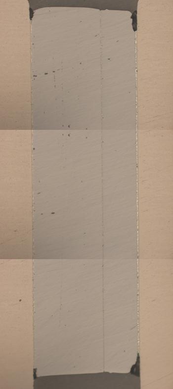
4 Cross-sectioning Diode D21 was cross-sectioned for further investigation of the die. Shown below is the picture of the die sandwiched between the leads. The dark line inside the die was identified as a metallic layer with a definitive variation in thickness. Two subsequent picture series show the die area from top to bottom (next page, left image) and the active region of the die (next page, right image).
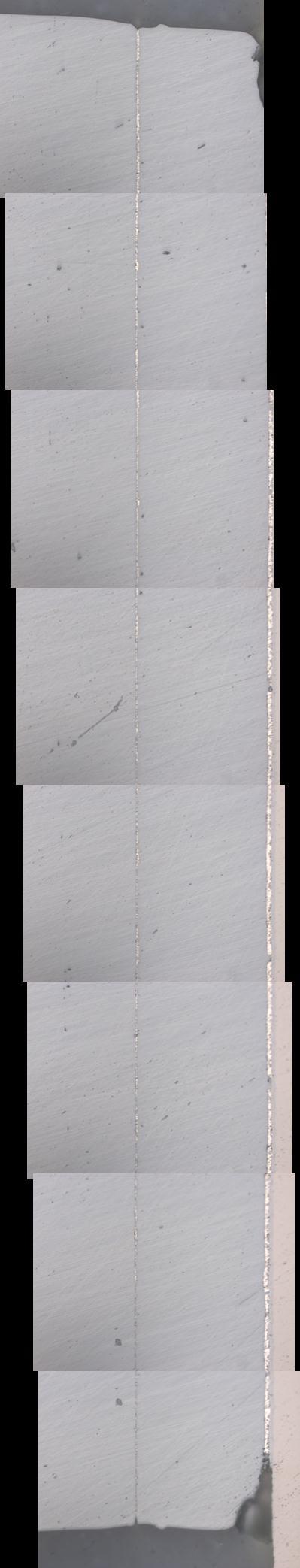
5

6 Failure Site DFR Solutions performed sequential cross sectioning on D21 with curve tracing performed in between grinding/polishing steps. Cross sectioning proceeded to the center of the diode without any change in the curve trace signature. Just beyond the center of the diode the curve trace showed that the fault was no longer present (see Figure 2). A finer polish was performed to see if any artifacts of the fault remained. A crack in the bulk silicon is visible (Figure 3). The loss of the failure signature by grinding a small distance further into the diode suggests a highly localized failure site of the short. Figure 2: Curve trace of diode D21; left, before grinding past failure site; right, after Figure 3: Failed Diode D21 after grinding past the main short
7 Current (A) The diode with approximately half of the area still present still exhibited a high reverse leakage current of -370μA at -160V (see Figure 4). This indicates the presence of a distribution of failure sites across the die, of which one failed catastrophically. 0.00E+00 Reverse Bias Diode D21 after grinding past the main failure site -5.00E E E E E E E-04 Diode D E E E Voltage (V) Figure 4: Measurements of reverse leakage current after grinding past failure site Electron Microscopy Energy dispersive spectroscopy (EDS) performed during examination by electron microscopy identified silver as the primary element in the metallic layer. A small amount of gold was also identified. As can be seen in the figure to the right, gold energy transition peaks at kev (Au Mα) and at kev (Au Lα 1 ) are evident in Spectrum 3 and Spectrum 2. The image resolution of Spectrum 1 is unfortunately insufficient to clearly prove the presence of gold in the silicon, but the Au Mα peak seems to be present. Gold is known to be used as a dopant in fast-recovery diodes. While contamination of silver does not necessarily lead to a strong degradation of the diode properties, contamination with gold is known to degrade the junction performance severely..
8 Diffusivity (cm 2 /sec) Metal contamination Metal contamination of silicon can occur throughout the fabrication process. Impurities can be introduced by contaminated wafer handling, improper surface or etching treatments, by the presence of a contaminated gas atmosphere during high temperature treatments, or by inappropriate post-processing of metallized devices. The influence of these contaminants will depend on the type of contaminant, its concentration, and the environmental parameters, time and temperature, the silicon device experiences after exposure to the contaminant. Silicon p-n diodes are the oldest and one of the most common of all semiconductor devices. A p-n diode is created by doping silicon wafers with Group III elements (such as boron) to create p-type layers and Group V elements (such as phosphorous) to create n-type layers. Silicon power diodes are also more susceptible because their manufacture requires higher temperatures and longer diffusion times compared to standard semiconductor technology. Additional steps after wafer production, such as welding and glass sealing, can also involve temperatures high enough to induce the diffusion of excessive amounts of impurities. Crystallographic defects present in the silicon, such as vacancies, dislocations, and stacking faults, can have a large effect on the solubility and diffusivity of transition metal impurities. As a result, the solubilities and diffusivities provided in Figure 5 and Figure 6 are based upon research-level purity silicon wafers and are not necessarily appropriate for silicon wafers with different defect characteristics. Taking the bulk diffusivity values in Figure 5 and assuming Fickian behavior, it can be seen that the present interface metals silver and gold will all easily diffuse to the junction of the silicon die over the time and temperatures used during the bonding and glass sealing processes 1.E-04 1.E-05 1.E-06 Cu Au i Ni Fe Ag i 1.E-07 1.E-08 Ti 1.E-09 1.E-10 Au s 1.E-11 1.E Temperature ( o C) Figure 5: The diffusivity of transition metals in silicon. Au i is the interstitial diffusivity of gold in silicon; Au s is the substitutional diffusivity of gold in silicon; Ag i is the interstitial diffusivity of silver in silicon 2. 2 Klaus Graff, Metal Impurities in Silicon-Device Fabrication, Springer-Verlag, Berlin (1995)
9 Solubility (cm -3 ) 1E+18 1E+17 Cu Ni Au s 1E+16 1E+15 Ag i 1E+14 1E+13 Au i Fe Ti 1E+12 1E Temperature ( o C) Figure 6: Solubility of transition metals in silicon. Au i is the interstitial solubility of gold in silicon; Au s is the substitutional solubility of gold in silicon; Ag i is the interstitial solubility of silver in silicon 2. Because the solubility has a steep temperature dependence, upon cooling from high temperatures the transition metal atoms will tend to exceed their saturation limit in silicon. In response to the changing equilibrium condition and the increasing driving force to nucleate, the impurity atoms can exhibit four different behaviors: The impurity atoms will diffuse to the surface of diode (outdiffusion) and form precipitates at the surface. This process requires a high diffusion rate, such as found in nickel and copper (see Figure 5). The impurity atoms will precipitate within the bulk of silicon. For homogeneous nucleation, a high diffusion rate and high solubility are necessary. For heterogeneous nucleation, a high diffusion rate and the presence of crystallographic defects are required. The impurity atom remains dissolved within the bulk of the silicon. This process requires low diffusion rates coupled with high cooling rates. Dissolved impurities are electrically active and form deep energy levels within the silicon band gap. The impurity atoms form complexes with other impurities present in the silicon. These complexes are unstable and will result in changes in the electrical behavior with variations in the external stimuli, i.e., temperature, current, etc.
10 The following paragraphs will review the influence of silver, and gold on the electrical properties of p-n diodes. Silver Silver is also a fast diffuser in silicon (see Figure 5). Silver acts as a singly ionizable donor in p- and n-type silicon. In p-type silicon, the donor level is 0.26eV above the valence band; in n-type silicon, the acceptor level is 0.29eV below the conduction band. Previous work has found that at room temperature. Because the capture cross-section at room temperature for silver atoms is low [2], carrier mobilities and carrier lifetimes in silicon diodes are relatively unaffected by the introduction of large concentrations of silver. Gold Because gold acts as a strong recombination center in silicon, it has been widely used as a dopant to control minority carrier lifetime and improve the speed of semiconductor devices. However, the unintended doping of silicon with gold can lead to the degradation of important electrical properties. Tolerable gold impurity content during wafer production is often much less than cm -3, which necessitates the use of Deep Level Transient Spectroscopy (DLTS) for impurity detection. Concerns about gold impurity have led to stricter quality control during wafer processing and replacement of gold as a rear contact material. These steps have led to a reduction in the frequency of excessive gold contamination. The contamination of silicon with gold is easily performed by the mechanical contact of gold with silicon because gold rapidly migrates into silicon, even at low temperatures (< 800 C). As an example, Mielke 3 and Makhkamov 4 measured a three orders of magnitude increase in the gold concentration in silicon, from cm -3 to approximately cm -3, after a heat treatment of 800 C for one hour. This high diffusion rate is in part due to the formation of a gold-silicon eutectic at 370 C. With increasing temperatures, this liquid phase acts as a rapid diffusion source. Gold diffusion in silicon occurs by an interstitial-substitutional process. The diffusivity of interstitial gold is very high while the solubility is low. The reverse is true for substitutional gold, which has a low diffusivity and a high solubility 5. The net result is that the diffusive flux is carried almost entirely by interstitial diffusion. The interstitials can then combine with vacancies in the silicon lattice to form substitutional defects. These substitutional gold defects are electrically active and will tend to have the greatest effect on the electrical properties of the p-n diode. [2] Two orders of magnitude lower than gold. 3 W. Mielke, "Penentration of Gold and Platinum Through Phosphorous-Doped N+ Layers in Silicon," Journal of the Electrochemical Society, vol. 122, no. 7, pp (1975) 4 S. Makhkamov, N.A. Tursunov, M. Mamanova, and M. Ashurov, "The Effect of a New Gold Center on the Characteristics of Silicon Diodes," Soviet Tech. Phys. Letters, vol. 17, no. 12, pp (1991) 5 Substitutional gold diffusion and solubility is strongly dependent upon crystal perfection and the presence other defects. As a result, diffusivity and solubility measurements for homogeneous silicon cannot be applied indiscriminately to silicon with other defect characteristics or to all regions of a particular device.
11 Gold tends to have a greater influence on junction behavior than other transition metals, because the position of acceptor energy level for substitutional gold in n-type silicon, -0.54eV below the conduction band edge or in the middle of the band gap, makes gold a very effective recombination center. In addition, since gold introduces both a deep donor and acceptor in silicon, it decreases the net carrier concentration in both p-type and n-type material. Gold can also combine with iron impurities already present in the silicon crystal to create irongold complexes. These iron-gold complexes form between C and can result in a reduction in the carrier lifetime by a factor of five in comparison to substitutional gold of equal concentration. It is therefore important to avoid the formation of iron-gold pairs. This requires avoiding gold contamination, since iron is almost always present in silicon wafers, at least in low concentrations. A summary of previous work on the effect of gold on the electrical properties of silicon diodes is provided below: Resisitivity Gold increases the resistivity of silicon diodes by decreasing the net carrier concentration 6. Reverse Leakage Current The leakage current in gold doped silicon can be estimated from I = qwante t p, where q is the electronic charge, W is the depletion width, A is the area of the diode, Nt is the gold concentration, and e t p is the thermal emission rate of holes from neutral acceptors 7,8 (see Figure 7). The reverse current at 1000V at 180 C was found to increase from 4 ma to 130 ma after diffusing gold into silicon at 865 C. Diffusion time and gold concentration were not provided 9. Due to increases in the leakage current with increasing temperature, for a gold dopant level of 2x10 14 cm -3, silicon p + -n diodes will become unstable at 150 C 8. 6 E.D. Wolley and R. Stickler, "Formation of Precipitates in Gold Diffused Silicon," Journal of Electrochemical Society, vol. 114, no. 12, pp (1967) 7 W.M. Bullis, "Properties of Gold in Silicon," Solid-State Electronics, vol. 9, pp (1966). 8 M.D. Miller, "Differences Between Platinum- and Gold-Doped Silicon Power Devices," IEEE Trans. Electron Devices, vol. ED-23, no. 12, p , (1976) 9 B.J. Baliga and E. Sun, "Comparison of Gold, Platinum, and Electron Irradiation for Controlling Lifetime in Power Rectifiers," IEEE Trans. Electron Devices, vol. ED-24, no. 6, p , (1977)
12 Reverse Current (Amps) 1.E-02 1.E-03 1.E-04 1.E-05 1.E-06 1.E Temperature ( o C) Applied Voltage: 800V Gold Concentration: 2x10 14 cm -3 Area of the Diode: cm 2 Depletion Width: 100 m Figure 7: The predicted leakage current for gold doped silicon p+-n diode as a function of junction temperature 8 Breakdown Voltage The addition of gold for a p + -n junction results in a reduction in the electric field. For breakdown to occur, the electric field must reach a critical value. Therefore, the breakdown voltage of p + -n silicon diodes will increase with gold doping 10 (see Figure 8). The breakdown voltage of golddoped p + -n silicon diodes changes with frequency 11. There is a sharp decrease in the breakdown voltage in n + -p silicon diodes for gold diffusion temperatures greater than 800 C 12 (see Figure 9). The gold doping of silicon decreases the low-current (20 μa) breakdown voltage in n + -p diodes. Can also cause localized avalanche breakdowns, resulting in I-V curves with double break characteristics D.K. Schroder, "Impedance and Other Properties of Gold Doped Silicon P-N Junctions," Thesis. University of Illinois. (1968) 11 K. Kijima, H. Gamo, and S. Ohsaki, "Frequency Dependence of the Breakdown Voltage of Gold-Doped Si P+N junctions," Electrochemical Society Fall Meeting - Battery Division, New York, NY, p , (1974) 12 T. Ogawa, "Influence of Metal Impurities on Breakdown Characteristics of High Voltage Silicon n+p Junctions," Japanese Journal of Applied Physics, vol. 5, no. 2, pp (1966) 13 J.M Fairfield and B.V. Gokhale, "Control of Diffused Diode Recovery Time Through Gold Doping," Solid-State Electronics, vol. 9, pp , (1966)
13 Breakdown Voltage (V) Reverse Leakage Current (Amps) Breakdown Voltage (V) p + -n silicon mesa diode n + -p silicon mesa diode Diffusion Temperature ( o C) Figure 8: Change in breakdown voltage as a function of gold diffusion temperature 10. Device characteristics: Junction area was 4.5x10⁻³ cm2; junction depth was approximately 2.5 microns; diffusion time was 48 hours. Over the diffusion temperatures selected, C, gold concentration ranged from 1x10 14 to 1x10 16 cm E Breakdown Voltage 1.E E E E E-05 0 Reverse Current Diffusion Temperature ( o C) 1.E-06 Figure 9: Change in breakdown voltage and leakage current as a function of diffusion temperature in gold-doped n + -p silicon diodes. Breakdown voltage was defined as a reverse current of 3 µa for samples with sharp I-V characteristics and 1mA for devices with soft I-V characteristics (>800 C). Reverse current was measured at 900V. Diffusion time was 1 hour.
14 Forward Current Forward current is also dependent upon gold concentration. The dependency is linear or square root depending if low current or high current densities 7. Junction Capacitance The transition capacitance of silicon p-n diodes is frequency independent. When gold is added, the junction capacitance of gold-doped p + -n diodes becomes frequency dependent 14 and varies with gold concentration C.T. Sah and V.G. Reddi, Transactions of the Institute of Electrical and Electronic Engineers, vol. ED-11, pp. 345 (1964)
15 Summary Cross-sectioning of the diode showed the failure sites being distributed across the die, with a catastrophic failure (150Ω) occurring very localized at one of those sites. A review of the EDS data shows the presence of silver and gold close to the diode region. The silver is present in the die attach between the two dies, which is expected as silver is a common conductor in commercial die attach material. Since gold is frequently used as a dopant for fast recovery diodes, it is not clear whether the gold is present as part of the silver attach or as a dopant. Gold is known to diffuse easily into the p-n region of a diode. The effects of gold contamination are among others reduction in reverse breakdown voltage and increased reverse leakage current, as well as increase in forward bias resistivity. Given the evidence of multiple failure sites, the presence of gold is the likely root-cause of diode failure and its presence in the critical regions of the die should be confirmed through the use of secondary ion mass spectroscopy (SIMS)
16 Disclaimer DfR represents that a reasonable effort has been made to ensure the accuracy and reliability of the information within this report. However, DfR Solutions makes no warranty, both express and implied, concerning the content of this report, including, but not limited to the existence of any latent or patent defects, merchantability, and/or fitness for a particular use. DfR will not be liable for loss of use, revenue, profit, or any special, incidental, or consequential damages arising out of, connected with, or resulting from, the information presented within this report. Confidentiality The information contained in this document is considered to be proprietary to DfR Solutions and the appropriate recipient. Dissemination of this information, in whole or in part, without the prior written authorization of DfR Solutions, is strictly prohibited.
R Sensor resistance (Ω) ρ Specific resistivity of bulk Silicon (Ω cm) d Diameter of measuring point (cm)
 ρ Specific resistivity of bulk Silicon (Ω cm) d Diameter of measuring point (cm)") 4 Silicon Temperature Sensors 4.1 Introduction The KTY temperature sensor developed by Infineon Technologies is based on the principle of the Spreading Resistance. The expression Spreading Resistance derives
4 Silicon Temperature Sensors 4.1 Introduction The KTY temperature sensor developed by Infineon Technologies is based on the principle of the Spreading Resistance. The expression Spreading Resistance derives
Learning Objectives. Chapter Outline. Solidification of Metals. Solidification of Metals
 Learning Objectives Study the principles of solidification as they apply to pure metals. Examine the mechanisms by which solidification occurs. - Chapter Outline Importance of Solidification Nucleation
Imperfections: Good or Bad? Structural imperfections (defects) Compositional imperfections (impurities)
 Compositional imperfections (impurities)") Imperfections: Good or Bad? Structural imperfections (defects) Compositional imperfections (impurities) 1 Structural Imperfections A perfect crystal has the lowest internal energy E Above absolute zero
Imperfections: Good or Bad? Structural imperfections (defects) Compositional imperfections (impurities) 1 Structural Imperfections A perfect crystal has the lowest internal energy E Above absolute zero
Radiation Defects and Thermal Donors Introduced in Silicon by Hydrogen and Helium Implantation and Subsequent Annealing
 Solid State Phenomena Vols. 131-133 (2008) pp. 201-206 online at http://www.scientific.net (2008) Trans Tech Publications, Switzerland Online available since 2007/10/25 Radiation Defects and Thermal Donors
Defects and Diffusion
 Defects and Diffusion Goals for the Unit Recognize various imperfections in crystals Point imperfections Impurities Line, surface and bulk imperfections Define various diffusion mechanisms Identify factors
Implant Metrology for Bonded SOI Wafers Using a Surface Photo-Voltage Technique
 Implant Metrology for Bonded SOI Wafers Using a Surface Photo-Voltage Technique Adam Bertuch a, Wesley Smith a, Ken Steeples a, Robert Standley b, Anca Stefanescu b, and Ron Johnson c a QC Solutions Inc.,
Fabrication Technology
 Fabrication Technology By B.G.Balagangadhar Department of Electronics and Communication Ghousia College of Engineering, Ramanagaram 1 OUTLINE Introduction Why Silicon The purity of Silicon Czochralski
Citation for the original published paper (version of record):
:") http://www.diva-portal.org This is the published version of a paper published in Energy Procedia. Citation for the original published paper (version of record): Boulfrad, Y., Lindroos, J., Inglese, A.,
http://www.diva-portal.org This is the published version of a paper published in Energy Procedia. Citation for the original published paper (version of record): Boulfrad, Y., Lindroos, J., Inglese, A.,
Formation, evolution, and annihilation of interstitial clusters in ion-implanted Si
 PHYSICAL REVIEW B, VOLUME 63, 195206 Formation, evolution, and annihilation of interstitial clusters in ion-implanted Si Sebania Libertino and Salvatore Coffa CNR-IMETEM, Stradale Primosole 50, I-95121
Project III. 4: THIN FILM DEVICES FOR LARGE AREA ELECTRONICS
 Project III. 4: THIN FILM DEVICES FOR LARGE AREA ELECTRONICS Project leader: Dr D.N. Kouvatsos Collaborating researchers from other projects: Dr D. Davazoglou Ph.D. candidates: M. Exarchos, L. Michalas
Free Electron Model What kind of interactions hold metal atoms together? How does this explain high electrical and thermal conductivity?
 Electrical Good conductors of heat & electricity Create semiconductors Oxides are basic ionic solids Aqueous cations (positive charge, Lewis acids) Reactivity increases downwards in family Mechanical Lustrous
Transmission Mode Photocathodes Covering the Spectral Range
 Transmission Mode Photocathodes Covering the Spectral Range 6/19/2002 New Developments in Photodetection 3 rd Beaune Conference June 17-21, 2002 Arlynn Smith, Keith Passmore, Roger Sillmon, Rudy Benz ITT
TOPIC 2. STRUCTURE OF MATERIALS III
 Universidad Carlos III de Madrid www.uc3m.es MATERIALS SCIENCE AND ENGINEERING TOPIC 2. STRUCTURE OF MATERIALS III Topic 2.3: Crystalline defects. Solid solutions. 1 PERFECT AND IMPERFECT CRYSTALS Perfect
Free Electron Model What kind of interactions hold metal atoms together? How does this explain high electrical and thermal conductivity?
 Electrical Good conductors of heat & electricity Create semiconductors Oxides are basic ionic solids Aqueous cations (positive charge, Lewis acids) Reactivity increases downwards in family Free Electron
Point Defects. Vacancies are the most important form. Vacancies Self-interstitials
 Grain Boundaries 1 Point Defects 2 Point Defects A Point Defect is a crystalline defect associated with one or, at most, several atomic sites. These are defects at a single atom position. Vacancies Self-interstitials
Fe doped Magnetic Nanodiamonds made by Ion
 Fe doped Magnetic Nanodiamonds made by Ion Implantation ChienHsu Chen a, I.C. Cho b, Hui-Shan Jian c and H. Niu a* a Nuclear Science and Technology Development Center, National Tsing Hua University, HsinChu
National Semiconductor LM2672 Simple Switcher Voltage Regulator
 Construction Analysis National Semiconductor LM2672 Simple Switcher Voltage Regulator Report Number: SCA 9712-570 Global Semiconductor Industry the Serving Since 1964 17350 N. Hartford Drive Scottsdale,
CHAPTER 5 IMPERFECTIONS IN SOLIDS PROBLEM SOLUTIONS
 CHAPTER 5 IMPERFECTIONS IN SOLIDS PROBLEM SOLUTIONS Vacancies and Self-Interstitials 5.1 Calculate the fraction of atom sites that are vacant for copper at its melting temperature of 1084 C (1357 K). Assume
1. Introduction. What is implantation? Advantages
 Ion implantation Contents 1. Introduction 2. Ion range 3. implantation profiles 4. ion channeling 5. ion implantation-induced damage 6. annealing behavior of the damage 7. process consideration 8. comparison
Long-term reliability of SiC devices. Power and Hybrid
 Long-term reliability of SiC devices Power and Hybrid Rob Coleman Business Development and Applications Manager TT electronics, Power and Hybrid Roger Tall Product Specialist Charcroft Electronics Ltd
Performance and Radiation Resistance of Quantum Dot Multi-Junction Solar Cells
 B.C. Richards 1, Young Lin 1, Pravin Patel 1, Daniel Chumney 1, Paul R. Sharps 1 Chris Kerestes 1,2, David Forbes 2, Kristina Driscoll 2, Adam Podell 2, Seth Hubbard 2 1 EMCORE Corporation, Albuquerque,
The Nernst-Einstein equation indicates that the ratio β /D for a given material varies only with temperature. Calculate β/d for oxygen ions in Zr 0.
 The Nernst-Einstein equation indicates that the ratio β /D for a given material varies only with temperature. Calculate β/d for oxygen ions in 0.8 Y 0.2 1.9 at 800 C. 1 The Nernst-Einstein equation indicates
2007 Elsevier Science. Reprinted with permission from Elsevier.
 J. Härkönen, E. Tuovinen, P. Luukka, H.K. Nordlund, and E. Tuominen, Magnetic Czochralski silicon as detector material, Nuclear Instruments and Methods in Physics Research A 579 (2007) 648 652. 2007 Elsevier
Radiation Tolerant Isolation Technology
 Radiation Tolerant Isolation Technology Background The following contains a brief description of isolation technologies used for radiation hardened integrated circuits. The technologies mentioned are junction
LANDOLT-BÖRNSTEIN. Zahlenwerte und Funktionen aus Naturwissenschaften und Technik. Neue Serie. Gesamtherausgabe: K.-H. Hellwege O.
 LANDOLT-BÖRNSTEIN Zahlenwerte und Funktionen aus Naturwissenschaften und Technik Neue Serie Gesamtherausgabe: K.-H. Hellwege O. Madelung Gruppe III: Kristall- und Festkörperphysik Band 17 Halbleiter Herausgeber:
Electrical Properties of Ultra Shallow p Junction on n type Si Wafer Using Decaborane Ion Implantation
 Mat. Res. Soc. Symp. Proc. Vol. 686 2002 Materials Research Society Electrical Properties of Ultra Shallow p Junction on n type Si Wafer Using Decaborane Ion Implantation Jae-Hoon Song, Duck-Kyun Choi
Doping and Silicon Reference: Chapter 4 Jaeger or Chapter 3 Ruska
 Doping and Silicon Reference: Chapter 4 Jaeger or Chapter 3 Ruska Recalll dopants in silicon (column IV element) Column V extra electrons N type dopant N D P Phospherus, As Arsenic & Sb Antimony most common
CdTe and CdZnTe Crystal Growth and Production of Gamma Radiation Detectors
 CdTe and CdZnTe Crystal Growth and Production of Gamma Radiation Detectors Uri Lachish, guma science, P.O. Box 2104, Rehovot 76120, Israel Abstract Bridgman CdTe and CdZnTe crystal growth, with cadmium
N-PERT BACK JUNCTION SOLAR CELLS: AN OPTION FOR THE NEXT INDUSTRIAL TECHNOLOGY GENERATION?
 N-PERT BACK JUNCTION SOLAR CELLS: AN OPTION FOR THE NEXT INDUSTRIAL TECHNOLOGY GENERATION? Bianca Lim *, Till Brendemühl, Miriam Berger, Anja Christ, Thorsten Dullweber Institute for Solar Energy Research
Definition and description of different diffusion terms
 Definition and description of different diffusion terms efore proceeding further, it is necessary to introduce different terms frequently used in diffusion studies. Many terms will be introduced, which
IMP EPD End Point Detector
 IMP EPD End Point Detector An overview of the Hiden Analytical SIMS end point detector system for ion beam etch applications IMP-EPD Presentation Topics The topics covered in the presentation include:
Section 4: Thermal Oxidation. Jaeger Chapter 3. EE143 - Ali Javey
 Section 4: Thermal Oxidation Jaeger Chapter 3 Properties of O Thermal O is amorphous. Weight Density =.0 gm/cm 3 Molecular Density =.3E molecules/cm 3 O Crystalline O [Quartz] =.65 gm/cm 3 (1) Excellent
IEEE TRANSACTIONS ON NUCLEAR SCIENCE, VOL. 55, NO. 4, AUGUST
 IEEE TRANSACTIONS ON NUCLEAR SCIENCE, VOL. 55, NO. 4, AUGUST 2008 1833 Radiation Effects in MOS Oxides James R. Schwank, Fellow, IEEE, Marty R. Shaneyfelt, Fellow, IEEE, Daniel M. Fleetwood, Fellow, IEEE,
Newsletter. Test Services & Failure Analysis Laboratory. April The Reality of Flip-Chip Solder Bump Electromigration Failure INSIDE THIS ISSUE
 Test Services & Failure Analysis Laboratory April 2008 Newsletter INSIDE THIS ISSUE Features Solder Bump Electromigration Failure Solder Joint Failure Criteria External Inspection of PCBs Hollow Fibers
PHOTOVOLTAIC SOLAR ENERGY POLYCRYSTALLINE MODULES - SI-ESF-M-P156-60
 Solar Innova uses the latest materials to manufacture photovoltaic modules. Our modules are ideal for any application that uses the photoelectric effect as a clean energy source because of its minimal
Kinetics. Rate of change in response to thermodynamic forces
 Kinetics Rate of change in response to thermodynamic forces Deviation from local equilibrium continuous change T heat flow temperature changes µ atom flow composition changes Deviation from global equilibrium
Chemistry 145 Exam number 4 name 11/19/98 # Faraday s constant is 96,500 c/mole of electrons.
 Chemistry 145 Exam number 4 name 11/19/98 # Faraday s constant is 96,500 c/mole of electrons. A.(16) An electrochemical cell is prepared with a strip of manganese metal dipping in to a 1.0 M MnSO 4 solution
Chapter 1.6. Polished Single-Crystal Silicon, Prime Wafers (all numbers nominal) Wafer Specification Table. Diameter 100 mm 4-inch 150 mm 6-inch
 Wafer Specification Table. Diameter 100 mm 4-inch 150 mm 6-inch") Chapter 1.6 I - Substrate Specifications Polished Single-Crystal Silicon, Prime Wafers (all numbers nominal) Wafer Specification Table Diameter 100 mm 4-inch 150 mm 6-inch Thickness 525 µm 20.5 mils 675
Chapter 1.6 I - Substrate Specifications Polished Single-Crystal Silicon, Prime Wafers (all numbers nominal) Wafer Specification Table Diameter 100 mm 4-inch 150 mm 6-inch Thickness 525 µm 20.5 mils 675
2006 UPDATE METROLOGY
 INTERNATIONAL TECHNOLOGY ROADMAP FOR SEMICONDUCTORS METROLOGY THE ITRS DEVED AND INTENDED FOR TECHNOLOGY ASSESSMENT ONLY AND WITHOUT REGARD TO ANY COMMERCIAL CONSIDERATIONS PERTAINING TO INDIVIDUAL PRODUCTS
Alloys and Solid Solutions
 Alloys and Solid Solutions Chemistry 123 Spring 2008 Dr. Woodward Solutions Solid Solution 14 Carat Gold Liquid Solution Vodka Gaseous Solution Air Solution = A homogeneous mixture 1 Alloys An alloy is
Deformation Twinning in Bulk Aluminum with Coarse Grains
 Proceedings of the 12th International Conference on Aluminium Proceedings Alloys, of the September 12th International 5-9, 2010, Yokohama, Conference Japan on 2010 Aluminum The Japan Alloys, Institute
Dallas Semicoductor DS80C320 Microcontroller
 Construction Analysis Dallas Semicoductor DS80C320 Microcontroller Report Number: SCA 9702-525 Global Semiconductor Industry the Serving Since 1964 15022 N. 75th Street Scottsdale, AZ 85260-2476 Phone:
CHAPTER 5 IMPERFECTIONS IN SOLIDS PROBLEM SOLUTIONS ev /atom = exp. kt ( =
 CHAPTER 5 IMPERFECTIONS IN SOLIDS PROBLEM SOLUTIONS Vacancies and Self-Interstitials 5.1 Calculate the fraction of atom sites that are vacant for copper at its melting temperature of 1084 C (1357 K). Assume
Increased Efficiency and Improved Reliability in ORing functions using Trench Schottky Technology
 Increased Efficiency and Improved Reliability in ORing functions using Trench Schottky Technology Davide Chiola, Stephen Oliver, Marco Soldano International Rectifier, El Segundo, USA. As presented at
Solar Energy Research Institute of Singapore (SERIS), National University of Singapore (NUS), Singapore
, National University of Singapore (NUS), Singapore") MODELLING AND CHARACTERIZATION OF BBr3 BORON DIFFUSION PROCESS FOR N-TYPE SI WAFER SOLAR CELLS LI Mengjie 1, 2, a, HOEX Bram 3, MA Fa-Jun 3, DEVAPPA SHETTY Kishan 1, ABERLE Armin G. 1, 2, SAMUDRA Ganesh
MODELLING AND CHARACTERIZATION OF BBr3 BORON DIFFUSION PROCESS FOR N-TYPE SI WAFER SOLAR CELLS LI Mengjie 1, 2, a, HOEX Bram 3, MA Fa-Jun 3, DEVAPPA SHETTY Kishan 1, ABERLE Armin G. 1, 2, SAMUDRA Ganesh
Ph.D. Admission 20XX-XX Semester X
 Ph.D. Admission 20XX-XX Semester X Written Examination Materials Science & Engineering Department, IIT Kanpur Date of Examination: XX XXXX 20XX Timing: XX:XX XX:XX XX Application# Please read these instructions
Ferroelectric Oxide Single-Crystalline Layers by Wafer Bonding and Hydrogen/Helium Implantation
 Mat. Res. Soc. Symp. Proc. Vol. 748 2003 Materials Research Society U11.8.1 Ferroelectric Oxide Single-Crystalline Layers by Wafer Bonding and Hydrogen/Helium Implantation Ionut Radu, Izabela Szafraniak,
Isolation Technology. Dr. Lynn Fuller
 ROCHESTER INSTITUTE OF TECHNOLOGY MICROELECTRONIC ENGINEERING Isolation Technology Dr. Lynn Fuller Motorola Professor 82 Lomb Memorial Drive Rochester, NY 14623-5604 Tel (585) 475-2035 Fax (585) 475-5041
ELECTRICAL RESISTIVITY AS A FUNCTION OF TEMPERATURE
 ELECTRICAL RESISTIVITY AS A FUNCTION OF TEMPERATURE Introduction The ability of materials to conduct electric charge gives us the means to invent an amazing array of electrical and electronic devices,
Excimer Laser Annealing of Hydrogen Modulation Doped a-si Film
 Materials Transactions, Vol. 48, No. 5 (27) pp. 975 to 979 #27 The Japan Institute of Metals Excimer Laser Annealing of Hydrogen Modulation Doped a-si Film Akira Heya 1, Naoto Matsuo 1, Tadashi Serikawa
Silicon Oxides: SiO 2
 Silicon Oxides: SiO 2 Uses: diffusion masks surface passivation gate insulator (MOSFET) isolation, insulation Formation: grown / native thermal: highest quality anodization deposited: C V D, evaporate,
2. High Efficiency Crystalline Si Solar Cells
 2 High Efficiency Crystalline Si Solar Cells Students: Karthick Murukesan, Sandeep S S, Meenakshi Bhaisare, Bandana Singha, Kalaivani S and Ketan Warikoo Faculty members: Anil Kottantharayil, B M Arora,
Measurement data at orders of magnitude lower cost than other techniques BENEFITS Simple UVC source ideal for compact sensors
 Optan The Optan Ball Lens, with integrated focusing optics, is the first choice for discerning professionals developing sensors and instruments in demanding measurement applications. Designed for and proven
Challenges of Silicon Carbide MOS Devices
 Indo German Winter Academy 2012 Challenges of Silicon Carbide MOS Devices Arjun Bhagoji IIT Madras Tutor: Prof. H. Ryssel 12/17/2012 1 Outline What is Silicon Carbide (SiC)? Why Silicon Carbide? Applications
Metallization. Typical current density ~10 5 A/cm 2 Wires introduce parasitic resistance and capacitance
 Metallization Interconnects Typical current density ~10 5 A/cm 2 Wires introduce parasitic resistance and capacitance RC time delay Inter-Metal Dielectric -Prefer low dielectric constant to reduce capacitance
Schottky Tunnel Contacts for Efficient Coupling of Photovoltaics and Catalysts
 Schottky Tunnel Contacts for Efficient Coupling of Photovoltaics and Catalysts Christopher E. D. Chidsey Department of Chemistry Stanford University Collaborators: Paul C. McIntyre, Y.W. Chen, J.D. Prange,
Fabrication, Electrical Characterization, and Annealing of Al/, Cu/, and Au/4H-SiC Schottky Diodes
 Clemson University TigerPrints All Theses Theses 12-2007 Fabrication, Electrical Characterization, and Annealing of Al/, Cu/, and Au/4H-SiC Schottky Diodes Nikhil Karkhanis Clemson University, nkarkha@clemson.edu
COMPATIBILITY OF THE ALTERNATIVE SEED LAYER (ASL) PROCESS WITH MONO- Si AND POLY-Si SUBSTRATES PATTERNED BY LASER OR WET ETCHING
 PROCESS WITH MONO- Si AND POLY-Si SUBSTRATES PATTERNED BY LASER OR WET ETCHING") COMPATIBILITY OF THE ALTERNATIVE SEED LAYER (ASL) PROCESS WITH MONO- Si AND POLY-Si SUBSTRATES PATTERNED BY LASER OR WET ETCHING Lynne Michaelson 1, Anh Viet Nguyen 2, Krystal Munoz 1, Jonathan C. Wang
COMPATIBILITY OF THE ALTERNATIVE SEED LAYER (ASL) PROCESS WITH MONO- Si AND POLY-Si SUBSTRATES PATTERNED BY LASER OR WET ETCHING Lynne Michaelson 1, Anh Viet Nguyen 2, Krystal Munoz 1, Jonathan C. Wang
PHOTOVOLTAIC SOLAR ENERGY POLYCRYSTALLINE MODULES - SI-ESF-M-BIPV-SM-P125-36
 Solar Innova uses the latest materials to manufacture photovoltaic modules. Our modules are ideal for any application that uses the photoelectric effect as a clean energy source because of its minimal
Photovoltaics under concentrated sunlight
 Photovoltaics under concentrated sunlight April 2, 2013 The University of Toledo, Department of Physics and Astronomy Principles and Varieties of Solar Energy (PHYS 4400) Reading assignment: Sections 9.4
Semiconductor Technology
 Semiconductor Technology von A bis Z Metallization www.halbleiter.org Contents Contents List of Figures List of Tables II III 1 Metallization 1 1.1 Requirements on metallization........................
COMPUTER SIMULATION AND EXPERIMENTAL RESEARCH OF CAST PISTON POROSITY
 Tome V (year 2007), Fascicole 2, (ISSN 1584 2665) COMPUTER SIMULATION AND EXPERIMENTAL RESEARCH OF CAST PISTON POROSITY D. KAKAS, L. KOVACEVIC, P. TEREK UNIVERSITY OF NOVI SAD, FACULTY OF TECHNICAL SCIENCES,
Quality and Reliability Report
 Quality and Reliability Report Product Qualification MAAM-008819 2mm 8-Lead PDFN Plastic Package QTR-0147 M/A-COM Technology Solutions Inc. 100 Chelmsford Street Lowell, MA 01851 Tel: (978) 656-2500 Fax:
Fast recovery Radiation Enhanced Diffusion (RED) Diode:
 Diode:") Fast recovery Radiation Enhanced Diffusion (RED) Diode: Palladium versus Platinum J. Vobecký 1,2, V. Záhlava 2, V. Komarnitskyy 2 1 ABB SWITZERLAND Ltd. SEMICONDUCTORS Fabrikstrasse 3, CH-5600 Lenzburg,
Fast recovery Radiation Enhanced Diffusion (RED) Diode: Palladium versus Platinum J. Vobecký 1,2, V. Záhlava 2, V. Komarnitskyy 2 1 ABB SWITZERLAND Ltd. SEMICONDUCTORS Fabrikstrasse 3, CH-5600 Lenzburg,
Silver and Sulfur: Case Studies, Physics, and Possible Solutions. C. Hillman, S. Binfield, J. Seppi, and J. Arnold DfR Solutions April 15, 2009
 Silver and Sulfur: Case Studies, Physics, and Possible Solutions C. Hillman, S. Binfield, J. Seppi, and J. Arnold DfR Solutions April 15, 2009 2004-2007 Introduction Silver is a common metal in electronics
State of the art quality of a GeOx interfacial passivation layer formed on Ge(001)
") APPLICATION NOTE State of the art quality of a Ox interfacial passivation layer formed on (001) Summary A number of research efforts have been made to realize Metal-Oxide-Semiconductor Field Effect Transistors
APPLICATION NOTE State of the art quality of a Ox interfacial passivation layer formed on (001) Summary A number of research efforts have been made to realize Metal-Oxide-Semiconductor Field Effect Transistors
Boron Diffusion and Silicon Self-Interstitial Recycling between SiGeC layers
 Mat. Res. Soc. Symp. Proc. Vol. 810 2004 Materials Research Society C3.5.1 oron Diffusion and Silicon Self-Interstitial Recycling between SiGeC layers M. S. Carroll 1 J. C. Sturm, Dept. of Electrical Engineering,
a) The self-diffusion coefficient of a metal with cubic structure can be expressed as
 The self-diffusion coefficient of a metal with cubic structure can be expressed as") EXERCISES KJM5120 Chapter 5; Diffusion 1. Random (self) diffusion a) The self-diffusion coefficient of a metal with cubic structure can be expressed as 1 n D = s 6 t 2 where n/t represents the jump frequency
EXERCISES KJM5120 Chapter 5; Diffusion 1. Random (self) diffusion a) The self-diffusion coefficient of a metal with cubic structure can be expressed as 1 n D = s 6 t 2 where n/t represents the jump frequency
Features. Benefits. Min Typical Max Min Max. OPTAN-250H-BL 245 nm 250 nm 255 nm 0.5 mw 1.0 mw. OPTAN-255H-BL 250 nm 255 nm 260 nm 0.5 mw 1.
 DATA SHEET OPTAN BALL LENS UVC LEDS IN A TO-39 PACKAGE WHICH OFFERS SUPERIOR LIGHT OUTPUT, EXCELLENT SPECTRAL QUALITY AND LONG LIFETIMES. AVAILABLE IN PEAK WAVELENGTHS FROM 25 nm-28 nm AND OPTICAL OUTPUT
Module-6. Dislocations and Strengthening Mechanisms
 Module-6 Dislocations and Strengthening Mechanisms Contents 1) Dislocations & Plastic deformation and Mechanisms of plastic deformation in metals 2) Strengthening mechanisms in metals 3) Recovery, Recrystallization
Formation and Annihilation of Hydrogen-Related Donor States in Proton-Implanted and Subsequently Plasma-Hydrogenated N-Type Float-Zone Silicon
 Formation and Annihilation of Hydrogen-Related Donor States in Proton-Implanted and Subsequently Plasma-Hydrogenated N-Type Float-Zone Silicon Reinhart Job, University of Hagen, Germany Franz-Josef Niedernostheide,
Effect of Growth Process on Polycrystalline Silicon Solar Cells Efficiency.
 Effect of Growth Process on Polycrystalline Silicon Solar Cells Efficiency. ZOHRA BENMOHAMED, MOHAMED REMRAM* Electronic department university of Guelma Département d Electronique Université mai 195 BP
C h a p t e r 4 : D e f e c t s i n C r y s t a l s
 C h a p t e r 4 : D e f e c t s i n C r y s t a l s...perfection's a gift of The gods, few can boast they possess it - and most Of you, my dears, don't. - Ovid, The Art of Love Chapter 4: Defects in Crystals...
Soft Magnetic Properties of Nanocystalline Fe Si B Nb Cu Rod Alloys Obtained by Crystallization of Cast Amorphous Phase
 Materials Transactions, Vol. 43, No. 9 (2002) pp. 2337 to 2341 c 2002 The Japan Institute of Metals EXPRESS REGULAR ARTICLE Soft Magnetic Properties of Nanocystalline Fe Si B Nb Cu Rod Alloys Obtained
Section 4: Thermal Oxidation. Jaeger Chapter 3
 Section 4: Thermal Oxidation Jaeger Chapter 3 Properties of O Thermal O is amorphous. Weight Density =.0 gm/cm 3 Molecular Density =.3E molecules/cm 3 O Crystalline O [Quartz] =.65 gm/cm 3 (1) Excellent
Schottky-Barrier-Height Modulation of Ni Silicide/Si Contacts by Insertion of Thin Er or Pt Layers
 Schottky-Barrier-Height Modulation of Ni Silicide/Si Contacts by Insertion of Thin Er or Pt Layers Yoshihisa Ohishi 1, Kohei Noguchi 1, Kuniyuki Kakushima 2, Parhat Ahmet 1, Kazuo Tsutsui 2, Nobuyuki Sugii
Experiment E: Martensitic Transformations
 Experiment E: Martensitic Transformations Introduction: The purpose of this experiment is to introduce students to a family of phase transformations which occur by shear rather than diffusion. In metals,
High-efficiency GaN-based light-emitting diodes fabricated with identical Ag contact formed on both n- and p-layers
 High-efficiency GaN-based light-emitting diodes fabricated with identical Ag contact formed on both n- and p-layers Munsik Oh and Hyunsoo Kim * School of Semiconductor and Chemical Engineering and Semiconductor
Doris Ehrt and Doris Möncke. Friedrich Schiller University of Jena, Otto-Schott-Institut, Fraunhoferstr. 6, D Jena, Germany,
 Charge transfer absorption of Fe 3+ and Fe + complexes and UV radiation induced defects in different glasses Doris Ehrt and Doris Möncke Friedrich Schiller University of Jena, Otto-Schott-Institut, Fraunhoferstr.
Reflow Profiling: Time a bove Liquidus
 Reflow Profiling: Time a bove Liquidus AIM/David Suraski Despite much research and discussion on the subject of reflow profiling, many questions and a good deal of confusion still exist. What is clear
9. Welding Defects 109
 9. Welding Defects 9. Welding Defects 109 Figures 9.1 to 9.4 give a rough survey about the classification of welding defects to DIN 8524. This standard does not classify existing welding defects according
BONDING OF MULTIPLE WAFERS FOR HIGH THROUGHPUT LED PRODUCTION. S. Sood and A. Wong
 10.1149/1.2982882 The Electrochemical Society BONDING OF MULTIPLE WAFERS FOR HIGH THROUGHPUT LED PRODUCTION S. Sood and A. Wong Wafer Bonder Division, SUSS MicroTec Inc., 228 SUSS Drive, Waterbury Center,
Quality and Reliability Report
 Quality and Reliability Report Product Qualification MASW-007921 2mm 8-Lead Plastic Package QTR-0148 M/A-COM Technology Solutions Inc. 100 Chelmsford Street Lowell, MA 01851 Tel: (978) 656-2500 Fax: (978)
Study of a Thermal Annealing Approach for Very High Total Dose Environments
 Study of a Thermal Annealing Approach for Very High Total Dose Environments S. Dhombres 1-2, J. Boch 1, A. Michez 1, S. Beauvivre 2, D. Kraehenbuehl 2, F. Saigné 1 RADFAC 2015 26/03/2015 1 Université Montpellier,
Rockwell R RF to IF Down Converter
 Construction Analysis Rockwell R6732-13 RF to IF Down Converter Report Number: SCA 9709-552 Global Semiconductor Industry the Serving Since 1964 17350 N. Hartford Drive Scottsdale, AZ 85255 Phone: 602-515-9780
BAR STRAIN GAGE DATA SEMICONDUCTOR BAR STRAIN GAGES DATA SHEET
 SEMICONDUCTOR BAR STRAIN GAGES DATA SHEET BAR STRAIN GAGE DATA BAR GAGE SCHEMATIC See Table for X, Y & Z dimensions X=Overall Length Y= Active Area Z= Width BAR SEMICONDUCTOR STRAIN GAGES Part Number Lead
Heatsink Optimization Nathan Blattau
 Heatsink Optimization Nathan Blattau Introduction Optimal design of a heatsink, meeting program targets for cost, weight, size, and performance, is one of the more challenging activities within most electronics
Unit 1 The Solid State
 Points to Remember Amorphous and Crystalline Solids Unit 1 The Solid State Amorphous- short range order, Irregular shape eg-glass Crystalline Solids- long range order, regular shape eg : NaCl Molecular
Fabrication of Ti-Ni-Zr Shape Memory Alloy by P/M Process
 Materials Transactions, Vol. 5, No. 1 (29) pp. 2446 to 245 #29 The Japan Institute of Metals Fabrication of Ti-Ni-Zr Shape Memory Alloy by P/M Process Akira Terayama 1, Koji Nagai 2; * and Hideki Kyogoku
GRAPHIC MANUFACTURING CAPABILITY Q217-18
 All features are design dependent and may not be achievable in combination Reduced Yield / Special values up ( or down ) to the standard limit are design and application dependent Standard features only
V I S H AY I N T E R T E C H N O L O G Y, I N C. Vishay Electro-Films. w w w. v i s h a y. c o m
 V I S H AY I N T E R T E C H N O L O G Y, I N C. Pattern Substrates Using Thin Film Technology Vishay Electro-Films Application-Specific Pattern Substrates P r e c i s i o n R e s i s t o r s C a p a b
Specimen Preparation Technique for a Microstructure Analysis Using the Focused Ion Beam Process
 Specimen Preparation Technique for a Microstructure Analysis Using the Focused Ion Beam Process by Kozue Yabusaki * and Hirokazu Sasaki * In recent years the FIB technique has been widely used for specimen
J = D C A C B x A x B + D C A C. = x A kg /m 2
 1. (a) Compare interstitial and vacancy atomic mechanisms for diffusion. (b) Cite two reasons why interstitial diffusion is normally more rapid than vacancy diffusion. (a) With vacancy diffusion, atomic
KGC SCIENTIFIC Making of a Chip
 KGC SCIENTIFIC www.kgcscientific.com Making of a Chip FROM THE SAND TO THE PACKAGE, A DIAGRAM TO UNDERSTAND HOW CPU IS MADE? Sand CPU CHAIN ANALYSIS OF SEMICONDUCTOR Material for manufacturing process
Figure 2.3 (cont., p. 60) (e) Block diagram of Pentium 4 processor with 42 million transistors (2000). [Courtesy Intel Corporation.
 (e) Block diagram of Pentium 4 processor with 42 million transistors (2000). [Courtesy Intel Corporation.") Figure 2.1 (p. 58) Basic fabrication steps in the silicon planar process: (a) oxide formation, (b) selective oxide removal, (c) deposition of dopant atoms on wafer, (d) diffusion of dopant atoms into exposed
Figure 2.1 (p. 58) Basic fabrication steps in the silicon planar process: (a) oxide formation, (b) selective oxide removal, (c) deposition of dopant atoms on wafer, (d) diffusion of dopant atoms into exposed
HBLED packaging is becoming one of the new, high
 Ag plating in HBLED packaging improves reflectivity and lowers costs JONATHAN HARRIS, President, CMC Laboratories, Inc., Tempe, AZ Various types of Ag plating technology along with the advantages and limitations
Available online at ScienceDirect. Energy Procedia 55 (2014 )
") Available online at www.sciencedirect.com ScienceDirect Energy Procedia 55 (2014 ) 618 623 4th International Conference on Silicon Photovoltaics, SiliconPV 2014 Cast silicon of varying purity for high
Available online at www.sciencedirect.com ScienceDirect Energy Procedia 55 (2014 ) 618 623 4th International Conference on Silicon Photovoltaics, SiliconPV 2014 Cast silicon of varying purity for high
Objective To study the time and temperature variations in the hardness of Al-4% Cu alloy on isothermal aging.
 EXPERIMENT 8 PRECIPITATION HARDENING IN 2024 ALUMINUM Objective To study the time and temperature variations in the hardness of Al-4% Cu alloy on isothermal aging. Introduction Materials can be hardened
Metallization. Typical current density ~105 A/cm2 Wires introduce parasitic resistance and capacitance
 Metallization Interconnects Typical current density ~105 A/cm2 Wires introduce parasitic resistance and capacitance RC time delay Inter-Metal Dielectric -Prefer low dielectric constant to reduce capacitance
Ivan Bazarov Physics Department, Cornell University. Fundamental processes in III-V photocathodes; application for high-brightness photoinjectors
 Ivan Bazarov Physics Department, Cornell University Fundamental processes in III-V photocathodes; application for high-brightness photoinjectors 07/21/09 I.V. Bazarov, III-V Photocathodes, ERL09 2 Contents