7-2E. Photonic crystals
|
|
|
- Buddy Hodges
- 6 years ago
- Views:
Transcription
1 7-2E. Photonic crystals Purdue Univ, Prof. Shalaev, Univ Central Florida, CREOL, Prof Kik,

2 3-D 2-D Λ 1-D


3
4
5
6
7
8
9 Consider a two-dimensional photonic crystal
10
11
12
13 Bloch theorem
14 Bloch theorem
15 Bloch theorem
16 Bloch theorem
17 Bloch theorem
18 Bloch theorem
19 Photonic Bandstructure Dispersion curve = Photonic band structure Bandgap #2 Bandgap (no transmission) Standing wave v group =0 Long wavelength limit: effective index
20 Dispersion curve = Photonic band structure
21 Remind the Dispersion Curve of Slab Waveguide Dispersion curve = Photonic band structure Because guiding modes redistribute themselves with frequency, for small ω, the dispersion curve of guiding modes approaches the cladding line; Band structure For large ω, it approaches the For large ω, it approaches the core line.
22 Dispersion curve = Photonic band structure
23 Origin of Photonic Band Gap (PBG) Light in 1-D photonic crystal H L H L H L Photonic band gap
24 Photonic band gap
25 Photonic band gap Bragg Reflection λ B = 2 nd Sin( θ ) λ B B ~2d k B 2π = = λ B π d


26 Photonic band gap Bragg Diffraction Wavelength corresponds to the period. Reflected waves are in phase. Wave does not propagate inside. Wavelength does not correspond to the period Reflected waves are not in phase. Wave propagates through.


27 Photonic band gap Electron Energy gap E 2 h 2 = h k 2m Gap in energy spectra of electrons arises in periodic structure
28 PBG formation Photonic band gap 1. Dispersion curve for free space 3. At the band edges, standing waves form, with the energy being either in the high or the low index regions 2. In a periodic system, y when half the wavelength corresponds to the periodicity λ 2 = a k = π a the Bragg effect prohibits photon propagation. 4. Standing waves transport no energy with zero group velocity
29 Dispersion relation Dispersion curve = Photonic band structure ω n 1 : high h index material n 2 : low index material 4. Standing waves transport no energy with zero group velocity Air standing band wave in n 2 n 1 n 2 n 1 n 2 n 1 n 2 n 1 Stop band bandgap standing wave in n 1 Dielectric band 0 π/a k
30 Dispersion Relation Dispersion curve = Photonic band structure Plot the dispersion curves for both the positive and the negative sides, and then shift the curve segments with k >π/a upward or downward one reciprocal lattice vectors. This reduced range of wave vectors is called the Brillouin zone
31 2-D Photonic Crystals 1. In 2-D PBG, different layer spacing, a, can be met along different direction. Strong interaction occurs when λ/2 = a. 2. PBG (Photonic band gap) = stop bands overlap in all directions
32 2D Photonic band structure Band Diagram Air band Stop band Dielectric band
33 2D Photonic band structure
34 2D Photonic band structure
35 2D Photonic band structure
36 2D Photonic band structure

")
37 Four Possible Functionalities of PBG 1. Use of Stop Band 1. Stop band 1. Stop Band: Use PBG as high reflectivity omni-directional mirror (PBG waveguides) ) Stop band


38 2. Dielectric band 2. Use of Dielectric Band 2. Dielectric Band: Uses the strong dispersion available in a photonic crystal (dispersion engineering with form birefringence) Dielectric band
39 2. Dielectric band
40 Remind the dispersion relation in bulk media 2. Dielectric band 1. In a homogeneous material in absence of material dispersion n(ω)=constant =n, the dispersion i diagram is simply a straight line: ω=kc/n. 2. In 2D systems, one can think of this line as a cone. For a given frequency ω, this cone becomes a constant frequency circle.
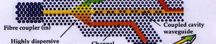
41 2. Dielectric band ky kx


42 Wave propagation in k-space 2. Dielectric band Real space The wave vector diagram tells us the direction and magnitude of the refracted and reflected beams. Their direction is normal to the iso-frequency curve and corresponds to Snell s law.
43 2. Dielectric band
44 2. Dielectric band
45 2. Dielectric band
46 2. Dielectric band
47 3. Air band 3. Use of Air Band 3. Air Band : Couples to radiative modes for light extraction from high-efficiency LEDs and fiber coupling. Air band
48 3. Air band


49 4. Defect band 4. Use of Defect Band 4. Defect Band : Couples to waveguide/cavity modes for spectral control such as PBG point defect laser or PBG line defect filter, etc. Defect band
50


51 Line Defect PBG Waveguide 4. Defect band Defect modes in stop band Dispersion diagram of W1 line-defect photonic crystal waveguide: Waveguide modes exist within the bandgap. Photons are prohibited in the 2D PBG, which lead to lossless confinement of photons in the line defect area.
52 Defects in PBG 4. Defect band
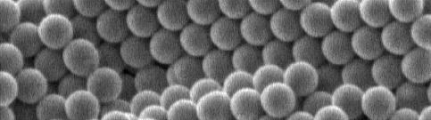
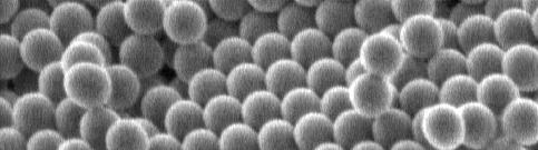
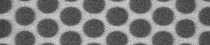
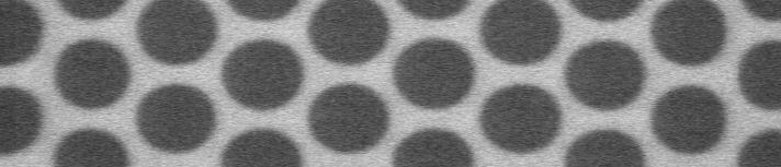
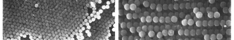
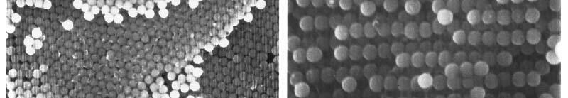
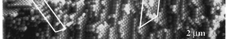
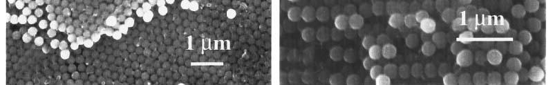
53 4. Defect band
54 4. Defect band
55 4. Defect band
56 4. Defect band


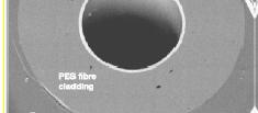
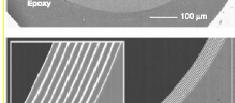
 K.")
 E.")
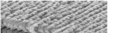
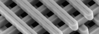
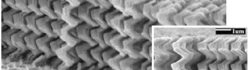
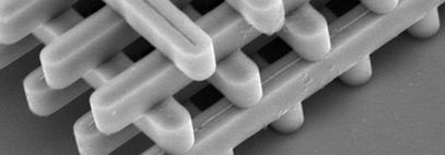
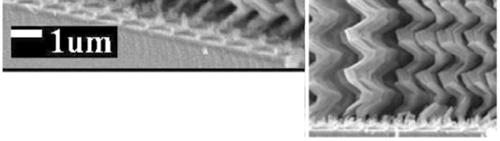
57 3D Photonic band structure 3D Photonic materials S.Noda, Nature (1999) K. Robbie, Nature (1996) E. Yablonovitch, PRL(1989)


58 Artificial Phonic Structure E.Yablonovitch et al., PRL (1987, 1991) 3D Photonic band structure Fabrication of artificial fcc material and band gap structure for such material.
59 Bragg diffraction through all electromagnetic region
60 Natural Opals


61 3D Photonic band structure Artificial Opal Artificial opal sample (SEM Image) Several cleaved planes of fcc structure are shown


62 Fabrication of artificial opals 3D Photonic band structure Silica spheres settle in close packed hexagonal layers There are 3 in-layer position A red; B blue; C green; Layers could pack in fcc lattice: ABCABC or ACBACB hcp lattice: ABABAB


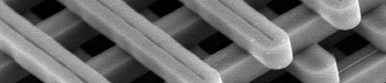
63 3D Photonic band structure Inverted Opals Inversed opals obtain greater dielectric contrast than opals.
64 3D Photonic band structure Band structure of diamond lattice Ph i b d f di d l i ( f i i d 3 45) Photonic band structure of diamond lattice (refractive index ~3.45) John et. al. PRE (1998)
65 Photonic Crystal Fibers PCF
66 PCF
67 The fiber supports a single mode over the range of at least nm! PCF
68 PCF
69 PCF
70 PCF
71 PCF
72 PCF
International Journal of Scientific & Engineering Research, Volume 6, Issue 2, February-2015 ISSN PHOTONIC CRYSTAL FIBER- AN OVERVIEW
 45 PHOTONIC CRYSTAL FIBER- AN OVERVIEW Neha Mahnot1, Shikha Maheshwary2, Rekha Mehra3 1, 2, 3 Govt. Engg. College, Ajmer 2 shikhasm1992@gmail.com 1 neha29mahnot@gmail.com Abstract- This review paper gives
Luminescent and Tunable 3D Photonic Crystal Structures
 Luminescent and Tunable 3D Photonic Crystal Structures Christopher J. Summers, E. Graugnard, D. Gaillot & J. S. King School of Materials Science and Engineering Georgia Institute of Technology Atlanta,
Chapter 3 Structure of Crystalline Solids
 Chapter 3 Structure of Crystalline Solids Crystal Structures Points, Directions, and Planes Linear and Planar Densities X-ray Diffraction How do atoms assemble into solid structures? (for now, focus on
Development of photonic and thermodynamic crystals conforming to sustainability conscious materials tectonics
 Sustainable Chemistry 103 Development of photonic and thermodynamic crystals conforming to sustainability conscious materials tectonics S. Kirihara, N. Ohta, T. Niki, Y. Uehara & S. Tasaki Joining and
High Pressure Chemical Vapor Deposition to make Multimaterial Optical Fibers
 High Pressure Chemical Vapor Deposition to make Multimaterial Optical Fibers Subhasis Chaudhuri *1 1, 2, 3, John V. Badding 1 Department of Chemistry, Pennsylvania State University, University Park, PA
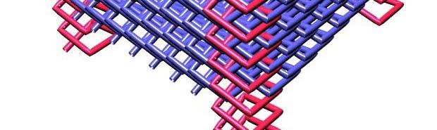
Optical properties of a three-dimensional silicon square spiral photonic crystal
 Photonics and Nanostructures Fundamentals and Applications xxx (2003) xxx xxx Optical properties of a three-dimensional silicon square spiral photonic crystal Scott R. Kennedy a,, Michael J. Brett a, Hernan
Engineering 45: Properties of Materials Final Exam May 9, 2012 Name: Student ID number:
 Engineering 45: Properties of Materials Final Exam May 9, 2012 Name: Student ID number: Instructions: Answer all questions and show your work. You will not receive partial credit unless you show your work.
Nanophotonics: principle and application. Khai Q. Le Lecture 11 Optical biosensors
 Nanophotonics: principle and application Khai Q. Le Lecture 11 Optical biosensors Outline Biosensors: Introduction Optical Biosensors Label-Free Biosensor: Ringresonator Theory Measurements: Bulk sensing
Simulation of Vector Mode Grating Coupler Interfaces for Integrated Optics. Chris Nadovich
 Simulation of Vector Mode Grating Coupler Interfaces for Integrated Optics Chris Nadovich Research Objective The novel combination of a forked holographic grating with a Bragg coupler structure to create
Basics of Plasmonics
 Basics of Plasmonics Min Qiu Laboratory of Photonics and Microwave Engineering School of Information and Communication Technology Royal Institute of Technology (KTH) Electrum 229, 16440 Kista, Sweden http://www.nanophotonics.se/
High Resolution X-ray Diffraction
 High Resolution X-ray Diffraction Nina Heinig with data from Dr. Zhihao Donovan Chen, Panalytical and slides from Colorado State University Outline Watlab s new tool: Panalytical MRD system Techniques:
Fs- Using Ultrafast Lasers to Add New Functionality to Glass
 An IMI Video Reproduction of Invited Lectures from the 17th University Glass Conference Fs- Using Ultrafast Lasers to Add New Functionality to Glass Denise M. Krol University of California, Davis 17th
Planar Defects in Materials. Planar Defects in Materials
 Classification of Defects in Solids: Planar defects: Stacking faults o {311} defects in Si o Inversion domain boundaries o Antiphase boundaries (e.g., super dislocations): analogous to partials but in
Experiment 2b X-Ray Diffraction* Optical Diffraction Experiments
 * Experiment 2b X-Ray Diffraction* Adapted from Teaching General Chemistry: A Materials Science Companion by A. B. Ellis et al.: ACS, Washington, DC (1993). Introduction Inorganic chemists, physicists,
Confocal Microscopy of Electronic Devices. James Saczuk. Consumer Optical Electronics EE594 02/22/2000
 Confocal Microscopy of Electronic Devices James Saczuk Consumer Optical Electronics EE594 02/22/2000 Introduction! Review of confocal principles! Why is CM used to examine electronics?! Several methods
11.3 The analysis of electron diffraction patterns
 11.3 The analysis of electron diffraction patterns 277 diameter) Ewald reflecting sphere, the extension of the reciprocal lattice nodes and the slight buckling of the thin foil specimens all of which serve
Steric Effects on the. Transition in YH x
 Steric Effects on the Metallic-Mirror Mirror to Transparent-Insulator Transition in YH x Troy C. Messina Department of Physics University of Texas at Austin Final Defense 22 November 2002 Outline Introduction
Solar Cells and Photosensors.
 Designing Photonic Crystals in Strongly Absorbing Material for Applications in Solar Cells and Photosensors. Minda Wagenmaker 1, Ebuka S. Arinze 2, Botong Qiu 2, Susanna M. Thon 2 1 Mechanical Engineering
nanosilicon Nanophotonics
 nanosilicon Nanophotonics Lorenzo Pavesi Universita di Trento Italy Outline Silicon Photonics NanoSilicon photonics Silicon Nanophotonics NanoSilicon Nanophotonics Conclusion Outline Silicon Photonics
2.1 µm CW Raman Laser in GeO 2 Fiber
 2.1 µm CW Raman Laser in GeO 2 Fiber B. A. Cumberland, S. V. Popov and J. R. Taylor Femtosecond Optics Group, Imperial College London, SW7 2AZ, United Kingdom O. I. Medvedkov, S. A. Vasiliev, E. M. Dianov
Tunable photonic bandgap structures for optical interconnects
 Optical Materials 27 (05) 740 744 www.elsevier.com/locate/optmat Tunable photonic bandgap structures for optical interconnects S.M. Weiss a, *, M. Haurylau b, P.M. Fauchet a,b a Institute of Optics, University
Coatings. Ion Assisted Deposition (IAD) process Advance Plasma Source (APS) plasma-ion assisted Deposition. Coatings on Optical Fibers
 process Advance Plasma Source (APS) plasma-ion assisted Deposition. Coatings on Optical Fibers") Anti-Reflection Custom Ion Assisted Deposition (IAD) process Advance Plasma Source (APS) plasma-ion assisted Deposition Anti-Reflection on Optical Fibers OptoSigma supplies a wide selection of optical
Anti-Reflection Custom Ion Assisted Deposition (IAD) process Advance Plasma Source (APS) plasma-ion assisted Deposition Anti-Reflection on Optical Fibers OptoSigma supplies a wide selection of optical
Theory of resonance and mode coupling in photonic crystal devices
 Theory of resonance and mode coupling in photonic crystal devices Thomas P. White A thesis submitted for the degree of Doctor of Philosophy Centre for Ultrahigh-bandwidth Devices for Optical Systems (CUDOS),
About Omics Group conferences
 About Omics Group OMICS Group International through its Open Access Initiative is committed to make genuine and reliable contributions to the scientific community. OMICS Group hosts over 400 leading-edge
Diffraction Basics. The qualitative basics:
 The qualitative basics: Diffraction Basics Coherent scattering around atomic scattering centers occurs when x-rays interact with material In materials with a crystalline structure, x-rays scattered in
CHAPTER 3: CRYSTAL STRUCTURES & PROPERTIES
 CHAPTER 3: CRYSTAL STRUCTURES & PROPERTIES ISSUES TO ADDRESS... How do atoms assemble into solid structures? (for now, focus on metals) How does the density of a material depend on its structure? When
Diffraction: Powder Method
 Diffraction: Powder Method Diffraction Methods Diffraction can occur whenever Bragg s law λ = d sin θ is satisfied. With monochromatic x-rays and arbitrary setting of a single crystal in a beam generally
Review key concepts from last lecture (lattice + basis = unit cell) Bravais lattices Important crystal structures Intro to miller indices
 Bravais lattices Important crystal structures Intro to miller indices") Outline: Review key concepts from last lecture (lattice + basis = unit cell) Bravais lattices Important crystal structures Intro to miller indices Review (example with square lattice) Lattice: square,
Outline: Review key concepts from last lecture (lattice + basis = unit cell) Bravais lattices Important crystal structures Intro to miller indices Review (example with square lattice) Lattice: square,
Standard Optics Information
 INFRASIL 301, 302 1. GENERAL PRODUCT DESCRIPTION Heraeus INFRASIL 301 and 302 are optical quartz glass grades manufactured by fusion of natural quartz crystals in an electrically heated furnace. They combine
Efficient, broadband and compact metal grating couplers for silicon-on-insulator waveguides
 Efficient, broadband and compact metal grating couplers for silicon-on-insulator waveguides Stijn Scheerlinck, Jonathan Schrauwen, Frederik Van Laere, Dirk Taillaert, Dries Van Thourhout and Roel Baets
Rare Earth Doped Fibers for Use in Fiber Lasers and Amplifiers
 Photonics Media Webinar: 4 th Nov 2013 Rare Earth Doped Fibers for Use in Fiber Lasers and Amplifiers George Oulundsen, Fiber Product Line Manager Bryce Samson, VP Business Development 1 Outline Introduction
Chapter Outline How do atoms arrange themselves to form solids?
 Chapter Outline How do atoms arrange themselves to form solids? Fundamental concepts and language Unit cells Crystal structures Face-centered cubic Body-centered cubic Hexagonal close-packed Close packed
PRECISION OPTICAL FILTERS BY EOSS - ENHANCED OPTICAL SPUTTERING SYSTEM. Fraunhofer
 PRECISION OPTICAL FILTERS BY EOSS - ENHANCED OPTICAL SPUTTERING SYSTEM EOSS ENHANCED OPTICAL SPUTTERING SYSTEM Fraunhofer IST, Braunschweig Contact: Dr. M. Vergöhl +49 531 2155 640 EOSS Coating System
Interferometric optical biosensor. Xingwei Wang
 Interferometric optical biosensor Xingwei Wang 1 Light Transverse electromagnetic wave Reflection Refraction Diffraction Interference 2 Fabry-Perot interferometer 3 Interferometer Two waves that coincide
First Electrically Pumped Hybrid Silicon Laser
 First Electrically Pumped Hybrid Silicon Laser UCSB Engineering Insights Oct 18 th 2006 Mario Paniccia Intel Corporation 1 Sept 18 th 2006 What We are Announcing Research Breakthrough: 1st Electrically
Polymer-based optical interconnects using nano-imprint lithography
 Polymer-based optical interconnects using nano-imprint lithography Arjen Boersma,Sjoukje Wiegersma Bert Jan Offrein, Jeroen Duis, Jos Delis, Markus Ortsiefer, Geert van Steenberge, MikkoKarppinen, Alfons
Efficient multi-mode to single-mode coupling in a photonic lantern
 Downloaded from orbit.dtu.dk on: Dec 15, 2017 Efficient multi-mode to single-mode coupling in a photonic lantern Noordegraaf, Danny; Skovgaard, Peter M.; Nielsen, Martin D.; Bland-Hawthorn, Jose Published
EBSD Basics EBSD. Marco Cantoni 021/ Centre Interdisciplinaire de Microscopie Electronique CIME. Phosphor Screen. Pole piece.
 EBSD Marco Cantoni 021/693.48.16 Centre Interdisciplinaire de Microscopie Electronique CIME EBSD Basics Quantitative, general microstructural characterization in the SEM Orientation measurements, phase
Inscription of first-order sapphire Bragg gratings using 400 nm femtosecond laser radiation
 Inscription of first-order sapphire Bragg gratings using 400 nm femtosecond laser radiation Tino Elsmann, 1,* Tobias Habisreuther, 1 Albrecht Graf, 1 Manfred Rothhardt, 1 and Hartmut Bartelt 1,2 1 Institute
Steps in solving a structure. Diffraction experiment. Obtaining well-diffracting crystals. Three dimensional crystals
 Protein structure from X-ray diffraction Diffraction images: ciprocal space Protein, chemical structure: IALEFGPSLKMNE Conformation, 3D-structure: CRYST1 221.200 73.600 80.900 90.00 90.00 90.00 P 21 21
SELF-POWERED FIBER BRAGG GRATING SENSORS. Benjamin W. McMillen. B.S. Electrical Engineering, University of Pittsburgh 2003
 SELF-POWERED FIBER BRAGG GRATING SENSORS by Benjamin W. McMillen B.S. Electrical Engineering, University of Pittsburgh 2003 Submitted to the Graduate Faculty of The School of Engineering in partial fulfillment
arxiv: v1 [physics.optics] 3 Feb 2010
![arxiv: v1 [physics.optics] 3 Feb 2010](/thumbs/72/66601340.jpg "arxiv: v1 [physics.optics] 3 Feb 2010") Plasmonic crystal demultiplexer and multiports Aurelien Drezet, Daniel Koller, Andreas Hohenau, Alfred Leitner, Franz R. Aussenegg, and Joachim R. Krenn Institute of Physics and Erwin Schrödinger Institute
Plasmonic crystal demultiplexer and multiports Aurelien Drezet, Daniel Koller, Andreas Hohenau, Alfred Leitner, Franz R. Aussenegg, and Joachim R. Krenn Institute of Physics and Erwin Schrödinger Institute
Transmission Mode Photocathodes Covering the Spectral Range
 Transmission Mode Photocathodes Covering the Spectral Range 6/19/2002 New Developments in Photodetection 3 rd Beaune Conference June 17-21, 2002 Arlynn Smith, Keith Passmore, Roger Sillmon, Rudy Benz ITT
Modification of Glass by FS Laser for Optical/Memory Applications
 Modification of Glass by FS Laser for Optical/Memory Applications Kazuyuki Hirao and Kiyotaka Miura Department of Material Chemistry Kyoto University International Workshop on Scientific Challenges of
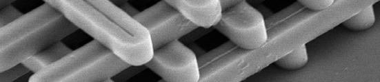
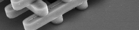
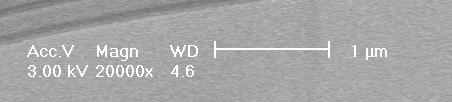
Supplementary Figure 1 Scanning electron micrograph (SEM) of a groove-structured silicon substrate. The micropillars are ca. 10 μm wide, 20 μm high
 of a groove-structured silicon substrate. The micropillars are ca. 10 μm wide, 20 μm high") Supplementary Figure 1 Scanning electron micrograph (SEM) of a groove-structured silicon substrate. The micropillars are ca. 10 μm wide, 20 μm high and own the gap of 10 μm. Supplementary Figure 2 Strictly
Supplementary Figure 1 Scanning electron micrograph (SEM) of a groove-structured silicon substrate. The micropillars are ca. 10 μm wide, 20 μm high and own the gap of 10 μm. Supplementary Figure 2 Strictly
Low-Loss Grating-Coupled Silicon Ridge Waveguides and Ring Resonators for Optical Gain at Telecommunication Frequencies
 Low-Loss Grating-Coupled Silicon Ridge Waveguides and Ring Resonators for Optical Gain at Telecommunication Frequencies J. P. Balthasar Müller Science Institute, University of Iceland, Dunhaga 3, IS-107
Single-polarization ultra-large-mode-area Ybdoped photonic crystal fiber
 Single-polarization ultra-large-mode-area Ybdoped photonic crystal fiber O. Schmidt, J. Rothhardt, T. Eidam, F. Röser, J. Limpert, A. Tünnermann Friedrich-Schiller University, Institute of Applied Physics,
Nanostructure Fabrication Using Laser Interference Lithography
 Nanostructure Fabrication Using Laser Interference Lithography ANTONIO JOU XIE, Class of 2012, Major: Electrical Engineering Mentor: SANG-WOO SEO, Professor, Electrical Engineering ABSTRACT: The constructive
Photoluminescence Spectroscopy on Chemically Synthesized Nanoparticles
 Photoluminescence Spectroscopy on Chemically Synthesized Nanoparticles Torben Menke 1 Institut für Angewandte Physik und Zentrum für Mikrostrukturforschung Universität Hamburg Diploma Talk, 18.12.27 1
High Gain Coefficient Phosphate Glass Fiber Amplifier
 High Gain Coefficient Phosphate Glass Fiber Amplifier Michael R. Lange, Eddy Bryant Harris Corp. Government Communications Systems Division P.O. Box 37 (MS: 13-9116) Melbourne, FL 3292 Michael J. Myers,
Optimization of dual-core and microstructure fiber geometries for dispersion compensation and large mode area
 Optimization of dual-core and microstructure fiber geometries for dispersion compensation and large mode area A. Huttunen Department of Electrical and Communications Engineering, Laboratory of Computational
BRAGG SCATTERING FROM COLLOIDAL CRYSTALS
 BRAGG SCATTERING FROM COLLOIDAL CRYSTALS In this experiment you have the opportunity to study the structure of microscopic crystals made of polystyrene spheres in water. By measuring the angles at which
UNIT V -CRYSTAL STRUCTURE
 UNIT V -CRYSTAL STRUCTURE Solids are of two types: Amorphous and crystalline. In amorphous solids, there is no order in the arrangement of their constituent atoms (molecules). Hence no definite structure
SPDT Effects on Surface Quality & Subsurface Damage in Ceramics
 SPDT Effects on Surface Quality & Subsurface Damage in Ceramics Deepak Ravindra & John Patten (Manufacturing Research Center- Western Michigan University) Jun Qu (Oak Ridge National Laboratory) Presentation
Digital resolution enhancement in surface plasmon microscopy
 Digital resolution enhancement in surface plasmon microscopy I.I. Smolyaninov 1) *, J. Elliott 2), G. Wurtz 2), A.V. Zayats 2), C.C. Davis 1) 1) Department of Electrical and Computer Engineering, University
Plasmonics: Application-oriented fabrication. Part 1. Introduction
 Plasmonics: Application-oriented fabrication Part 1. Introduction Victor Ovchinnikov Department of Aalto Nanofab Aalto University Espoo, Finland Alvar Aalto was a famous Finnish architect and designer
Electron microscopy II
 Electron microscopy II Nanomaterials characterization I RNDr. Věra Vodičková, PhD. Interaction ction: electrons solid matter Signal types SE.secondary e - AE Auger s e - BSE back scattered e - X-ray photons,
Mono/dual-polarization refractive-index biosensors with enhanced sensitivity based on annular photonic crystals
 arxiv:1405.5771 [physics.bio-ph] 23 May 2014 Mono/dual-polarization refractive-index biosensors with enhanced sensitivity based on annular photonic crystals Liyong Jiang 1,2,*, Hong Wu 1,3, We Zhang 1,
Plasmonic Nanostructures II
 Plasmonic Nanostructures II Dr. Krüger / Prof. M. Zacharias, IMTEK, Propagation of SPPs Propagation distance decreases with decreasing strip width! 2 Dr. Krüger / Prof. M. Zacharias, IMTEK, Bound and leaky
Introduction to Engineering Materials ENGR2000 Chapter 3: The Structure of Crystalline Solids. Dr. Coates
 Introduction to Engineering Materials ENGR2000 Chapter 3: The Structure of Crystalline Solids Dr. Coates Learning Objectives I 1. Describe difference in atomic/molecular structure between crystalline/noncrystalline
JECP/HOLZ, an Interactive Computer Program for Simulation of HOLZ Pattern
 JECP/HOLZ, an Interactive Computer Program for Simulation of HOLZ Pattern (Version 2t) X.Z. Li, Ph. D Copyright(C) 2002-2017 LANDYNE All Rights Reserved. Contents: 1. Purpose of the program 2. Graphic
OMICS Group signed an agreement with more than International Societies to make healthcare informati on Open Access. OMICS Group Conferences
 About Omics Group OMICS Group International through its Open Ac cess Initiative is committed to make genuine an d reliable contributions to the scientific commu nity. OMICS Group hosts over 400 leading-edg
Fundamental concepts and language Unit cells Crystal structures! Face-centered cubic! Body-centered cubic! Hexagonal close-packed Close packed
 Fundamental concepts and language Unit cells Crystal structures! Face-centered cubic! Body-centered cubic! Hexagonal close-packed Close packed crystal structures Density computations Crystal structure
Topological crystalline insulators. Tomasz Story Institute of Physics, Polish Academy of Sciences, Warsaw
 Topological crystalline insulators Tomasz Story Institute of Physics, Polish Academy of Sciences, Warsaw Topological crystalline insulators - outline 1. Introduction topological crystalline insulators
Presented at the 28th European PV Solar Energy Conference and Exhibition, 30 September 4 October, 2013, Paris, France
 INTEGRATING DIFFRACTIVE REAR SIDE STRUCTURES FOR LIGHT TRAPPING INTO CRYSTALLINE SILICON SOLAR CELLS J. Eisenlohr 1*, H. Hauser 1, J. Benick 1, A. Mellor 2, B. Bläsi 1, J.C. Goldschmidt 1, M. Hermle 1
Gotas Cuánticas (QD) de Semiconductores II-VI preparadas por ciclos de presión
 de Semiconductores II-VI preparadas por ciclos de presión") *C.E.S., Facultad de Ciencias, Departamento de Física, Universidad de Los Andes Mérida, Venezuela **Physique des Millieux Condenses (UA782), Tour 13, E4. Université P. et M. Curie, 4 Place Jussieu 75252,
*C.E.S., Facultad de Ciencias, Departamento de Física, Universidad de Los Andes Mérida, Venezuela **Physique des Millieux Condenses (UA782), Tour 13, E4. Université P. et M. Curie, 4 Place Jussieu 75252,
Symmetry in crystalline solids.
 Symmetry in crystalline solids. Translation symmetry n 1,n 2,n 3 are integer numbers 1 Unitary or primitive cells 2D 3D Red, green and cyano depict all primitive (unitary) cells, whereas blue cell is not
Scintillating Optical Fibers
 Scintillating Optical Fibers Plastic Scintillating Fibers Saint-Gobain Crystals manufactures a variety of plastic scintillating, wavelength-shifting and light-transmitting fibers used for research and
Study on Infrared Absorption Characteristics of Ti and TiN x Nanofilms. Mingquan Yuan, Xiaoxiong Zhou, Xiaomei Yu
 10.119/1.36982 The Electrochemical Society Study on Infrared Absorption Characteristics of Ti and TiN x Nanofilms Mingquan Yuan, Xiaoxiong Zhou, Xiaomei Yu National Key Laboratory of Science and Technology
Surface Plasmon Resonance-like integrated sensor at terahertz frequencies for gaseous analytes.
 Surface Plasmon Resonance-like integrated sensor at terahertz frequencies for gaseous analytes. Alireza Hassani and Maksim Skorobogatiy maksim.skorobogatiy@polymtl.ca www.photonics.phys.polymtl.ca Engineering
Lectures on: Introduction to and fundamentals of discrete dislocations and dislocation dynamics. Theoretical concepts and computational methods
 Lectures on: Introduction to and fundamentals of discrete dislocations and dislocation dynamics. Theoretical concepts and computational methods Hussein M. Zbib School of Mechanical and Materials Engineering
3.46 OPTICAL AND OPTOELECTRONIC MATERIALS
 Badgap Engineering: Precise Control of Emission Wavelength Wavelength Division Multiplexing Fiber Transmission Window Optical Amplification Spectrum Design and Fabrication of emitters and detectors Composition
FABRICATION AND PROPERTIES OF GALLIUM METALLIC PHOTONIC CRYSTALS
 FABRICATION AND PROPERTIES OF GALLIUM METALLIC PHOTONIC CRYSTALS V.F. Kozhevnikov, M. Diwekar, V.P. Kamaev, J. Shi, and Z.V. Vardeny Physics Department, University of Utah, Salt Lake City, UT 84112 Gallium
Scintillating Optical Fibers
 Scintillating Optical Fibers Plastic Scintillating Fibers Saint-Gobain Crystals manufactures a variety of plastic scintillating, wavelength-shifting and light-transmitting fibers used for research and
Travaux Pratiques de Matériaux de Construction
 Travaux Pratiques de Matériaux de Construction Section Matériaux 6 ème semestre 2009 Etude de Matériaux Cimentaire Par Diffraction des Rayons X Responsable: Silke Ruffing E-Mail: silke.ruffing@epfl.ch
Chapter 16. Liquids and Solids. Chapter 16 Slide 1 of 87
 Chapter 16 Liquids and Solids Chapter 16 Slide 1 of 87 Chapter Preview Intramolecular forces determine such molecular properties as molecular geometries and dipole moments. Intermolecular forces determine
12: Band Structure Calculations
 The Nuts and Bolts of First-Principles Simulation 12: Band Structure Calculations Durham, 6th-13th December 2001 CASTEP Developers Group with support from the ESF ψ k Network Outline Introduction to band
Monolithic Microphotonic Optical Isolator
 Monolithic Microphotonic Optical Isolator Lei Bi, Juejun Hu, Dong Hun Kim, Peng Jiang, Gerald F Dionne, Caroline A Ross, L.C. Kimerling Dept. of Materials Science and Engineering Massachusetts Institute
Photorefractive properties of lithium niobate crystals doped with manganese
 Yang et al. Vol. 20, No. 7/July 2003/J. Opt. Soc. Am. B 1491 Photorefractive properties of lithium niobate crystals doped with manganese Yunping Yang and Demetri Psaltis Department of Electrical Engineering,
Design Optimization of Structural Parameters for Highly Sensitive Photonic Crystal Label-Free Biosensors
 Sensors 2013, 13, 3232-3241; doi:10.3390/s130303232 Article OPEN ACCESS sensors ISSN 1424-8220 www.mdpi.com/journal/sensors Design Optimization of Structural Parameters for Highly Sensitive Photonic Crystal
Twins & Dislocations in HCP Textbook & Paper Reviews. Cindy Smith
 Twins & Dislocations in HCP Textbook & Paper Reviews Cindy Smith Motivation Review: Outline Crystal lattices (fcc, bcc, hcp) Fcc vs. hcp stacking sequences Cubic {hkl} naming Hcp {hkil} naming Twinning
Quiz on Monday covering: -symmetry operations -notations of axes, vectors, and face notation -Miller indices
 OTHER ANNOUNCEMENTS Quiz on Monday covering: -symmetry operations -notations of axes, vectors, and face notation -Miller indices 2 nd Draft of References due Monday Field Trip Saturday 10/4 and Sunday
Primitive cells, Wigner-Seitz cells, and 2D lattices. 4P70, Solid State Physics Chris Wiebe
 Primitive cells, Wigner-Seitz cells, and 2D lattices 4P70, Solid State Physics Chris Wiebe Choice of primitive cells! Which unit cell is a good choice?! A, B, and C are primitive unit cells. Why?! D, E,
Growth Of TiO 2 Films By RF Magnetron Sputtering Studies On The Structural And Optical Properties
 Journal of Multidisciplinary Engineering Science and Technology (JMEST) Growth Of TiO 2 Films By RF Magnetron Sputtering Studies On The Structural And Optical Properties Ahmed K. Abbas 1, Mohammed K. Khalaf
This experiment is included in the upgrade packages: XRC 4.0 X-ray characteristics and XRS 4.0 X-ray structural analysis.
 Characteristic X-rays of copper TEP Related Topics X-ray tube, bremsstrahlung, characteristic radiation, energy levels, crystal structures, lattice constant, absorption, absorption edges, interference,
Longitudinally Graded Optical Fibers
 Clemson University TigerPrints All Theses Theses 5-2013 Longitudinally Graded Optical Fibers Alexander Evert Clemson University, alex.g.evert@gmail.com Follow this and additional works at: http://tigerprints.clemson.edu/all_theses
Physical structure of matter. Monochromatization of molybdenum X-rays X-ray Physics. What you need:
 X-ray Physics Physical structure of matter Monochromatization of molybdenum X-rays What you can learn about Bremsstrahlung Characteristic radiation Energy levels Absorption Absorption edges Interference
Phil Saunders, spacechannel.org
 Guidi with Phil Saunders, spacechannel.org ng Light Long-Range nge Plasmons Aloyse Degiron, Pierre Berini and David R. Smith Long-range surface plasmons are optical modes propagating along metallic circuits
ENGINEERING MATERIALS LECTURE #4
 ENGINEERING MATERIALS LECTURE #4 Chapter 3: The Structure of Crystalline Solids Topics to Cover What is the difference in atomic arrangement between crystalline and noncrystalline solids? What features
Experimental study of EDFA Gain-Block for Booster Amplifier at C-band regime
 Experimental study of EDFA Gain-Block for Booster Amplifier at C-band regime S.K. Bhadra *, M. Pal, M.C. Paul, R. Sen, P. Biswas, S. Bandyopadhyay, and K. Dasgupta Fibre Optics Laboratory, Central Glass
TEM Study of the Morphology Of GaN/SiC (0001) Grown at Various Temperatures by MBE
 Grown at Various Temperatures by MBE") TEM Study of the Morphology Of GaN/SiC (0001) Grown at Various Temperatures by MBE W.L. Sarney 1, L. Salamanca-Riba 1, V. Ramachandran 2, R.M Feenstra 2, D.W. Greve 3 1 Dept. of Materials & Nuclear Engineering,
TEM Study of the Morphology Of GaN/SiC (0001) Grown at Various Temperatures by MBE W.L. Sarney 1, L. Salamanca-Riba 1, V. Ramachandran 2, R.M Feenstra 2, D.W. Greve 3 1 Dept. of Materials & Nuclear Engineering,
TEM imaging and diffraction examples
 TEM imaging and diffraction examples Duncan Alexander EPFL-CIME 1 Diffraction examples Kikuchi diffraction Epitaxial relationships Polycrystalline samples Amorphous materials Contents Convergent beam electron
356 Index. NLSGM nanorods, 124
 Index A Ab initio pseudopotentials, 35 Acoustic phonon dispersion, 330, 336 Acoustic pressure, 337 Anodic alumina, 206 Armchair CNT chirality, 93 Asymptotic stiffness, 83 B Band gap, 174, 190, 201, 211,
Large mode area silicon microstructured fiber with robust dual mode guidance
 Large mode area silicon microstructured fiber with robust dual mode guidance N. Healy 1, J. R. Sparks 2, M. N. Petrovich 1, P. J. A. Sazio 1,J.V. Badding 2, and A. C. Peacock 1 1 Optoelectronics Research
Geometries and materials for subwavelength surface plasmon modes
 44 J. Opt. Soc. Am. A/ Vol. 1, No. 1/ December 004 Zia et al. Geometries and materials for subwavelength surface plasmon modes Rashid Zia, Mark D. Selker, Peter B. Catrysse, and Mark L. Brongersma Geballe
Energy and Packing. Materials and Packing
 Energy and Packing Non dense, random packing Energy typical neighbor bond length typical neighbor bond energy r Dense, regular packing Energy typical neighbor bond length typical neighbor bond energy r
HOLLOW-CORE PHOTONIC CRYSTAL FIBER REFRACTIVE INDEX SENSOR BASED ON MODAL INTERFERENCE
 HOLLOW-CORE PHOTONIC CRYSTAL FIBER REFRACTIVE INDEX SENSOR BASED ON MODAL INTERFERENCE N. F. Baharin 1, N. Sidek 1, S. M. A. Musa 1, A. I. Azmi 1, A. S. Abdullah 1, M. Y. M. Noor 1 and M. E. M. Roslan
Mode conversion in two-dimensional magneto-photonic crystal waveguide made by fully compatible optical sol-gel matrix
 Optica Applicata, Vol. XLVI, No. 4, 216 DOI: 1.5277/oa1645 Mode conversion in two-dimensional magneto-photonic crystal waveguide made by fully compatible optical sol-gel matrix AHMED KAHLOUCHE *, ABDESSELAM
Introduction to Electron Backscattered Diffraction. TEQIP Workshop HREXRD Feb 1 st to Feb 5 th 2016
 Introduction to Electron Backscattered Diffraction 1 TEQIP Workshop HREXRD Feb 1 st to Feb 5 th 2016 SE vs BSE 2 Ranges and interaction volumes 3 (1-2 m) http://www4.nau.edu/microanalysis/microprobe/interact-effects.html
Fine Structure and Magnetism of the Cubic Oxide Compound Ni 0.3 Zn 0.7 O
 ISSN 163-7834, Physics of the Solid State, 11, Vol. 53, No. 7, pp. 136 1366. Pleiades Publishing, Ltd., 11. Original Russian Text S.F. Dubinin, V.I. Maksimov, V.D. Parkhomenko, V.I. Sokolov, A.N. Baranov,