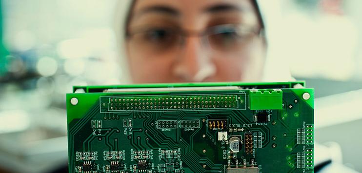
Annual Meeting. North Carolina State University Dr. Veena Misra. January 17 19, 2017 December
|
|
|
- Aileen Rosa Cole
- 6 years ago
- Views:
Transcription


1 Annual Meeting North Carolina State University Dr. Veena Misra January 17 19, 2017 December


2 Misra Group at NCSU Over 9 years experience in wide band gap research on SiC, GaN and Ga2O3. World leaders in atomic layer deposited (ALD) dielectrics for enhancing power device, logic, memory and sensor applications. SiC device research in PowerAmerica Device Development track The image cannot be displayed. Your computer may not have enough memory to open the image, or the image may have been corrupted. Restart your computer, and then open the file again. If the red x still appears, you may have to delete the image and then insert it again. 50 Capacitance [pf] 40 O3 Al2O3 H2O Al2O3 30 Al2O3 13nm PDA 400PMA RT CV 1MHz Vg [V]
3 Project Objectives The primary objectives are to: Demonstrate high mobility SiC MOSFETs based on incorporation of rare earth and high-k dielectrics using a manufacturable process flow for medium voltage (<1700V) power switch device application Key Performance measures: Reliability, mobility, threshold voltage and high temperature performance Broader impact on the WBG community: Our novel approach for SiC research provides 1) a fabrication cost reduction by achieving high mobility and 2) better gate stack reliability by process optimization and innovation. 3
4 Milestones and Deliverables Open foundry process & stability / reliability assessment Fabricate SiC MOSFET with ALD dielectric on foundry wafer (Month 12) V T shift < 0.4V under ± 4MV/cm stress at RT (Month 4) V T shift < 0.5V under ± 4MV/cm stress at 150 C (Month 7) TDDB and MTTF evaluation at RT (Month 7) V T shift < 0.5V under ± 4MV/cm stress at 150 C (Month 12) Optimizing gate stacks for mobility and rare earth dielectric: V T shift < 0.5V under ± 4MV/cm at RT (Month 6) and rare earth dielectric: V T shift < 0.5V under ± 4MV/cm at 150 C (Month 12) Lateral MOSFET with V T > 3V and mobility > 100 cm 2 /V s (Month 9) 4
5 Monthly progress and quarterly milestones Task Task/Subtask description Milestone Q1 Q2 Q3 Q Fabricate SiC DMOSFET with ALD dielectric on foundry wafer V T instability of in house lateral MOSFET V T instability of in house lateral MOSFET V T instability of MOSFET from foundry V T instability of MOSFET from foundry Long-term integrity/reliability evaluation Long-term integrity/reliability evaluation 2.1 Growth condition optimization 2.2 Process parameter optimization 2.3 V T instability of MOSFET with rare-earth oxide/ V T instability of MOSFET with rare-earth oxide/ Task 1. Open foundry process & stability/reliability assessment Mobility > 50 cm 2 /V s, V T shift < 0.5V V T shift < 0.4V under ±4MV/ cm (RT) V T shift < 0.5V under ±4MV/ cm (150 C) V T shift < 0.4V under ±4MV/ cm (RT) V T shift < 0.5V under ±4MV/ cm (150 C) TDDB and MTTF evaluation of ALD oxides (RT) TDDB and MTTF evaluation of ALD oxides (150 C) Task 2. Optimizing gate stacks for mobility > 100 cm 2 /V s Mobility and V T vs. thickness trade-off V T > 3V and Mobility > 100 cm 2 /V s V T shift < 0.5V under ±4MV/ cm (RT) V T shift < 0.5V under ±4MV/ cm (150 C) 5
6 SiC R&D: Introduction and Approach Current issues of SiC MOSFET Gate Source Thermal oxide Source p + n + n + p + p-well p-well V T control n-type drift layer n-type substrate Drain High interface states density (D it ) Carbon rich interfacial layer Clustered carbons Dangling bonds Poor mobility Poor mobility Mobility / Threshold voltage (V T ) trade-off 6
7 SiC R&D: Introduction and Approach Approach [1] LaSiO x : Control of mobility Gate Source La 2 SiO x Drain n + P-epi n + N + SiC [2] : Control of threshold voltage [1] Advantages of LaSiO x [2] Using on SiC Scavenging effect 1,2 Resistant to crystallization up to 900 C 1 No substrate oxidation Precise thickness control Ideal for trench MOSFETs Negative charge 1. J. -P. Maria et al., J. Appl. Phys., Vol. 90, No. 7, H. Iwai et al., IEDM Tech. Dig., pp ,

8 SiC MOSFET with La 2 O 3 / fabrication S/D implantation and activation La 2 O 3 deposition using a MBE tool 30nm deposition at 150 C substrate temperature Post deposition anneal (PDA) in N 2 O at 900 C Lateral MOSFET Gate Source La 2 SiO x Drain n + P-epi n + N + SiC Gate electrode deposition Contact hole etching La 2 O 3 PDA La 2 SiO x S/D Nickel deposition SiC SiC S/D silicide formation anneal at 950 C 4H-SiC, Si-face, 8 o off axis, p-type epi-layer doping 5E15cm -3 8
9 SiC MOSFET with La 2 O 3 / I DS V GS Characteristic Field Effect Mobility High mobility and positive threshold are achieved with LaO/SiO 2 dielectric Lateral MOSFET with La 2 O 3 give the higher mobility > 120cm 2 /V s 9

10 Reliability results (in BP1) PBTI Test at RT MOSFET with 0.3nm La 2 O 3 / - V T shift ~ 1.6V under 4MV/cm stress - Electron trapping in La-silicate à Need process optimization Our Approach Gate La 2 SiO x (0.3nm Source n + ) Drain n + P-epi N + SiC High temperature Rapid Thermal Annealing Forming Gas Anneal (RTA-FGA) to improve LaSiO x layer
11 La 2 O 3 0.3nm/ MOSFET : FGA effect Transfer characteristic Field-effect Mobility La 2 O 3 0.3nm/ : FGA reduces the V T and the improved mobility Gate La 2 SiO x (0.3nm Source n + ) Drain n + P-epi N + SiC 11
12 La 2 O 3 0.6nm/ MOSFET : FGA effect Transfer characteristic Field-effect Mobility La 2 O 3 0.6nm/ : FGA reduces the V T and the improved mobility Gate La 2 SiO x (0.6nm Source n + ) Drain n + P-epi N + SiC 12
13 La 2 O 3 1.0nm/ MOSFET : FGA effect Transfer characteristic Field-effect Mobility La 2 O 3 1.0nm/ : FGA not affect the V T and the mobility Gate La 2 SiO x (1.0nm Source n + ) Drain n + P-epi N + SiC 13
14 Summary of V T and mobility (After FGA) V T vs. La 2 O 3 thickness Mobility vs. La 2 O 3 thickness By inserting a LaSiO x layer at SiC/SiO 2 è Interface properties have been significantly improved è 1nm La 2 O 3 : V T > 3 V and mobility > 120cm 2 /V s Below 0.5nm La 2 O 3 : FGA improve the V T and the mobility 14
15 Optimization for better reliability : FGA Effect PBTI Test at RT high temperature 700 C and 800 C FGA give the best V T stability <0.5V under 4MV/cm stress V T shift significantly increases at high temperature Source Gate La 2 O 3 (T~0.3nm) P-epi Drain N + SiC 15
16 Reliability Results : La 2 O 3 varying thickness High Temperature Reliability Case 1. Trapping by Case 2. Out diffusion of hydrogen atoms H Interface trapped charge Diffusion LaSiO X SiC LaSiO X SiC H H H Si Si Si Si La 2 O 3 is known to contain bulk electron traps 1,2. Electrons in the channel tunnel into the traps. Electron trapping in La-silicate 2,3 Larger V T shift were observed at elevated temperature. Possible reasons Trapping by near the interface Access deeper trap at elevated temperature Out diffusion of hydrogen atoms 1. T. Kawanago et al, Microelectronic Engineering, 86, 7 9, 2009, 2. G. Lucovsky et al, J. Vac. Sci. Technol., B22, 2004, 3. N. Inoue et al, Jpn. J. Appl. Phys. 46,
17 SiC Summary and Future Direction Summary Demonstrated 4H SiC lateral MOSFET with V T > 3V and mobility > 120 cm 2 / V-s Demonstrated V T shift < 0.4 V under ± 4MV/cm constant DC stress ALD LaO/SiO 2 also confirms high mobility but further optimization is needed. Future Plans: (1) Further reliability study at elevated temperature (2) Continue on process optimization (3) Development of Open Process Modules with X-Fab 17
18 Pathway to Market Development of standard unit processes typically used in SiC device flows Access to foundry with standardized modules Development of non-exclusive gate dielectric processes Send ALD dielectrics to foundries for evaluation Reliability and Cost of new processes Need to make sure patent and licensing issues are not barriers Commercial grade (wafer size > 6 ) ALD tool acquisition will be beneficial for fast adoption of high mobility gate stack. 18
19 Aspirations for PowerAmerica How would you like to see the Institute evolve Provide the research community access to manufacturable tools to ensure relevance to foundries Recruit/collaborate with large equipment companies to become part of supply/chain of WBG Use equipment companies to solidify unit processes before transfer to foundries Most valuable role the Institute can play Develop a roadmap for SiC devices (like ITRS roadmap for Si) What you will do to help the Institute grow Focus on manufacturable SiC devices that provide enhancements in performance and cost and enable PA to gain leadership Support workforce development by training students in WBG research and development Unique opportunities/gaps the Institute can exploit Institute should exploit its large expertise of scientists on WBG Institute should come up with a model for sustainability beyond Year 5. 19
20 Project Title: Objec8ves: Open foundry process & stability / Major Milestones: reliability assessment, OpNmizing gate stacks for mobility Significant Equipment Acquisi8on: Deliverables: SiC Channel mobility enhancement Develop a key module process with foundry, achieve 5X higher mobility, evaluate long term stability, reliability SiC device with µ > 100cm 2 /V s, ΔV T < ± 0.4V under ±4MV stress and ΔV T < ± 0.5V under ±4MV stress at 150 C TPOC: Veena Misra vmisra@ncsu.edu, Phone: WBG Technology Impact 1. WBG SiC and provide high temperature, high voltage, and high speed operation. High mobility SiC and devices will further improve device property while reducing a die size and driver circuits resulting in cost advantages. 2. Medium voltage range applications (~1700V) such as automotive, industrial motors, consumer electronics, PV inverters, etc. 3. Timeframe for commercialization: BP-3 4. Improving SiC mobility by ~50% will reduce on-resistance by ~20% for power devices up to 1700V and result in smaller die size and cost. More WBG Impact and Additional impacts 1. Our technology can overcome the tradeoff in SiC mobility vs. threshold voltage. With our technology high V T (3V) is also achieved while maintaining high mobility (>100cm 2 /V s). 2. Today, researches of SiC MOSFET reliability raised significant concerns on the long-term operation of SiC MOS-based devices. We are focused on overcoming large threshold voltage shift at elevated temperature. PowerAmerica Date: January 2017
Electrical Characteristics of Rare Earth (La, Ce, Pr and Tm) Oxides/Silicates Gate Dielectric
 Oxides/Silicates Gate Dielectric") Electrical Characteristics of Rare Earth (La, Ce, Pr and Tm) Oxides/Silicates Gate Dielectric K. Matano 1, K. Funamizu 1, M. Kouda 1, K. Kakushima 2, P. Ahmet 1, K. Tsutsui 2, A. Nishiyama 2, N. Sugii
Electrical Characteristics of Rare Earth (La, Ce, Pr and Tm) Oxides/Silicates Gate Dielectric K. Matano 1, K. Funamizu 1, M. Kouda 1, K. Kakushima 2, P. Ahmet 1, K. Tsutsui 2, A. Nishiyama 2, N. Sugii
Effect of High Pressure Deuterium Annealing on Performance and Reliability of MOSFETs with High-k Gate Dielectrics and Metal Gate
 Effect of High Pressure Deuterium Annealing on Performance and Reliability of MOSFETs with High-k Gate Dielectrics and Metal Gate H. Park, M. Chang, H. Yang, M. S. Rahman, M. Cho, B.H. Lee*, R. Choi*,
Nagatsuta, Midori-ku, Yokohama , Japan. Technology, 4259-S2-20 Nagatsuta, Midori-ku, Yokohama , Japan
 Improvement of Interface Properties of W/La O 3 /Si MOS Structure Using Al Capping Layer K. Tachi a, K. Kakushima b, P. Ahmet a, K. Tsutsui b, N. Sugii b, T. Hattori a, and H. Iwai a a Frontier Collaborative
State of the art quality of a GeOx interfacial passivation layer formed on Ge(001)
") APPLICATION NOTE State of the art quality of a Ox interfacial passivation layer formed on (001) Summary A number of research efforts have been made to realize Metal-Oxide-Semiconductor Field Effect Transistors
APPLICATION NOTE State of the art quality of a Ox interfacial passivation layer formed on (001) Summary A number of research efforts have been made to realize Metal-Oxide-Semiconductor Field Effect Transistors
Reliability and Stability Issues for Lanthanum Silicate as a High-K Dielectric. Raleigh NC 27695, USA. Raleigh NC 27695, USA
 10.1149/1.2355716, copyright The Electrochemical Society Reliability and Stability Issues for Lanthanum Silicate as a High-K Dielectric Daniel J. Lichtenwalner a, Jesse S. Jur a, Steven Novak b, Veena
Advanced Gate Stack, Source/Drain, and Channel Engineering for Si-Based CMOS 6: New Materials, Processes, and Equipment
 Advanced Gate Stack, Source/Drain, and Channel Engineering for Si-Based CMOS 6: New Materials, Processes, and Equipment Editors: E. P. Gusev Qualcomm MEMS Technologies San Jose, California, USA D-L. Kwong
Memory Devices. Ki-Nam Kim, President, Institut of Technology Samsung Electronics, 2010 IEDM, San Francisco.
 Memory Devices In Korea now, Samsung : 2010, 30nm 2Gb DDRS DRAM/DDR3 SRAM 2011, Invest US $12 bil. for 20nm & SysLSI. Hynix : 2010, 26nm MLC- NAND Flash 2011, 30nm 4Gb DRAM At 2020, the demands of computing
Schottky-Barrier-Height Modulation of Ni Silicide/Si Contacts by Insertion of Thin Er or Pt Layers
 Schottky-Barrier-Height Modulation of Ni Silicide/Si Contacts by Insertion of Thin Er or Pt Layers Yoshihisa Ohishi 1, Kohei Noguchi 1, Kuniyuki Kakushima 2, Parhat Ahmet 1, Kazuo Tsutsui 2, Nobuyuki Sugii
Lecture 030 Integrated Circuit Technology - I (5/8/03) Page 030-1
 Page 030-1") Lecture 030 Integrated Circuit Technology - I (5/8/03) Page 030-1 LECTURE 030 INTEGRATED CIRCUIT TECHNOLOGY - I (References [7,8]) Objective The objective of this presentation is: 1.) Illustrate integrated
Lecture 030 Integrated Circuit Technology - I (5/8/03) Page 030-1 LECTURE 030 INTEGRATED CIRCUIT TECHNOLOGY - I (References [7,8]) Objective The objective of this presentation is: 1.) Illustrate integrated
Challenges of Silicon Carbide MOS Devices
 Indo German Winter Academy 2012 Challenges of Silicon Carbide MOS Devices Arjun Bhagoji IIT Madras Tutor: Prof. H. Ryssel 12/17/2012 1 Outline What is Silicon Carbide (SiC)? Why Silicon Carbide? Applications
Supplementary Figure S1 Crystal structure of the conducting filaments in sputtered SiO 2
 Supplementary Figure S1 Crystal structure of the conducting filaments in sputtered SiO 2 based devices. (a) TEM image of the conducting filament in a SiO 2 based memory device used for SAED analysis. (b)
Lecture 4. Oxidation (applies to Si and SiC only) Reading: Chapter 4
 Reading: Chapter 4") Lecture 4 Oxidation (applies to Si and SiC only) Reading: Chapter 4 Introduction discussion: Oxidation: Si (and SiC) Only The ability to grow a high quality thermal oxide has propelled Si into the forefront
Lecture 4 Oxidation (applies to Si and SiC only) Reading: Chapter 4 Introduction discussion: Oxidation: Si (and SiC) Only The ability to grow a high quality thermal oxide has propelled Si into the forefront
EE-612: Lecture 28: Overview of SOI Technology
 EE-612: Lecture 28: Overview of SOI Technology Mark Lundstrom Electrical and Computer Engineering Purdue University West Lafayette, IN USA Fall 2006 NCN www.nanohub.org Lundstrom EE-612 F06 1 outline 1)
Oxide Growth. 1. Introduction
 Oxide Growth 1. Introduction Development of high-quality silicon dioxide (SiO2) has helped to establish the dominance of silicon in the production of commercial integrated circuits. Among all the various
Radiation Tolerant Isolation Technology
 Radiation Tolerant Isolation Technology Background The following contains a brief description of isolation technologies used for radiation hardened integrated circuits. The technologies mentioned are junction
Silicon Wafer Processing PAKAGING AND TEST
 Silicon Wafer Processing PAKAGING AND TEST Parametrical test using test structures regularly distributed in the wafer Wafer die test marking defective dies dies separation die fixing (not marked as defective)
Isolation Technology. Dr. Lynn Fuller
 ROCHESTER INSTITUTE OF TECHNOLOGY MICROELECTRONIC ENGINEERING Isolation Technology Dr. Lynn Fuller Motorola Professor 82 Lomb Memorial Drive Rochester, NY 14623-5604 Tel (585) 475-2035 Fax (585) 475-5041
Wet Oxidation and Hydrogen Incorporation on 4H-SiC (c-face)
") Wet Oxidation and Hydrogen Incorporation on 4H-SiC (c-face) Can Xu 1, Voshadhi Amarasinghe 1, Gang Liu 1, Boris Yakshinskiy 1, Sarit har 2, Torgny Gustafsson 1, Joseph Bloch 1 and Leonard Feldman 1 1 Institute
Wet Oxidation and Hydrogen Incorporation on 4H-SiC (c-face) Can Xu 1, Voshadhi Amarasinghe 1, Gang Liu 1, Boris Yakshinskiy 1, Sarit har 2, Torgny Gustafsson 1, Joseph Bloch 1 and Leonard Feldman 1 1 Institute
Project III. 4: THIN FILM DEVICES FOR LARGE AREA ELECTRONICS
 Project III. 4: THIN FILM DEVICES FOR LARGE AREA ELECTRONICS Project leader: Dr D.N. Kouvatsos Collaborating researchers from other projects: Dr D. Davazoglou Ph.D. candidates: M. Exarchos, L. Michalas
Low temperature deposition of thin passivation layers by plasma ALD
 1 Low temperature deposition of thin passivation layers by plasma ALD Bernd Gruska, SENTECH Instruments GmbH, Germany 1. SENTECH in brief 2. Low temperature deposition processes 3. SENTECH SI ALD LL System
Laser Spike Annealing for sub-20nm Logic Devices
 Laser Spike Annealing for sub-20nm Logic Devices Jeff Hebb, Ph.D. July 10, 2014 1 NCCAVS Junction Technology Group Semicon West Meeting July 10, 2014 Outline Introduction Pattern Loading Effects LSA Applications
Protective Metal Oxides that Electronically Couple Catalysts to Efficient Light Absorbers
 Protective Metal Oxides that Electronically Couple Catalysts to Efficient Light Absorbers Co-PI: Christopher Chidsey Personnel: Andrew Scheuermann, Olivia Hendricks, and Kyle Kemp Support: GCEP Leverage:
Advanced CMOS Process Technology Part 3 Dr. Lynn Fuller
 MICROELECTRONIC ENGINEERING ROCHESTER INSTITUTE OF TECHNOLOGY Part 3 Dr. Lynn Fuller Webpage: http://people.rit.edu/lffeee Electrical and Microelectronic Engineering Rochester Institute of Technology 82
3.155J / 6.152J Micro/Nano Processing Technology TAKE-HOME QUIZ FALL TERM 2005
 3.155J / 6.152J Micro/Nano Processing Technology TAKE-HOME QUIZ FALL TERM 2005 1) This is an open book, take-home quiz. You are not to consult with other class members or anyone else. You may discuss the
Al 2 O 3 SiO 2 stack with enhanced reliability
 Al 2 O 3 SiO 2 stack with enhanced reliability M. Lisiansky, a A. Fenigstein, A. Heiman, Y. Raskin, and Y. Roizin Tower Semiconductor Ltd., P.O. Box 619, Migdal HaEmek 23105, Israel L. Bartholomew and
Atomic Layer Deposition of High-k k Dielectric and Metal Gate Stacks for MOS Devices
 International Conference on Characterization and Metrology for ULSI Technology March 15-18, 2005 Atomic Layer Deposition of High-k k Dielectric and Metal Gate Stacks for MOS Devices Yoshi Senzaki, Kisik
Contact Resistance Reduction using Advanced Implant and Anneal Techniques for 7nm Node and Beyond
 Contact Resistance Reduction using Advanced Implant and Anneal Techniques for 7nm Node and Beyond Fareen Adeni Khaja Global Product Manager, Front End Products Transistor and Interconnect Group NCCAVS
2. High Efficiency Crystalline Si Solar Cells
 2 High Efficiency Crystalline Si Solar Cells Students: Karthick Murukesan, Sandeep S S, Meenakshi Bhaisare, Bandana Singha, Kalaivani S and Ketan Warikoo Faculty members: Anil Kottantharayil, B M Arora,
EE40 Lec 22. IC Fabrication Technology. Prof. Nathan Cheung 11/19/2009
 Suggested Reading EE40 Lec 22 IC Fabrication Technology Prof. Nathan Cheung 11/19/2009 300mm Fab Tour http://www-03.ibm.com/technology/manufacturing/technology_tour_300mm_foundry.html Overview of IC Technology
CMOS FABRICATION. n WELL PROCESS
 CMOS FABRICATION n WELL PROCESS Step 1: Si Substrate Start with p- type substrate p substrate Step 2: Oxidation Exposing to high-purity oxygen and hydrogen at approx. 1000 o C in oxidation furnace SiO
New Materials as an enabler for Advanced Chip Manufacturing
 New Materials as an enabler for Advanced Chip Manufacturing Drive Innovation, Deliver Excellence ASM International Analyst and Investor Technology Seminar Semicon West July 10 2013 Outline New Materials:
2006 UPDATE METROLOGY
 INTERNATIONAL TECHNOLOGY ROADMAP FOR SEMICONDUCTORS METROLOGY THE ITRS DEVED AND INTENDED FOR TECHNOLOGY ASSESSMENT ONLY AND WITHOUT REGARD TO ANY COMMERCIAL CONSIDERATIONS PERTAINING TO INDIVIDUAL PRODUCTS
Portland Technology Development, * CR, # QRE, % PTM Intel Corporation
 A 45nm Logic Technology with High-k + Metal Gate Transistors, Strained Silicon, 9 Cu Interconnect Layers, 193nm Dry Patterning, and 100% Pb-free Packaging K. Mistry, C. Allen, C. Auth, B. Beattie, D. Bergstrom,
Semiconductor Technology
 Semiconductor Technology von A bis Z Metallization www.halbleiter.org Contents Contents List of Figures List of Tables II III 1 Metallization 1 1.1 Requirements on metallization........................
Long-term reliability of SiC devices. Power and Hybrid
 Long-term reliability of SiC devices Power and Hybrid Rob Coleman Business Development and Applications Manager TT electronics, Power and Hybrid Roger Tall Product Specialist Charcroft Electronics Ltd
Isolation of elements
 1 In an IC, devices on the same substrate must be isolated from one another so that there is no current conduction between them. Isolation uses either the junction or dielectric technique or a combination
Figure 2.3 (cont., p. 60) (e) Block diagram of Pentium 4 processor with 42 million transistors (2000). [Courtesy Intel Corporation.
 (e) Block diagram of Pentium 4 processor with 42 million transistors (2000). [Courtesy Intel Corporation.") Figure 2.1 (p. 58) Basic fabrication steps in the silicon planar process: (a) oxide formation, (b) selective oxide removal, (c) deposition of dopant atoms on wafer, (d) diffusion of dopant atoms into exposed
Figure 2.1 (p. 58) Basic fabrication steps in the silicon planar process: (a) oxide formation, (b) selective oxide removal, (c) deposition of dopant atoms on wafer, (d) diffusion of dopant atoms into exposed
Semiconductor Manufacturing Technology. IC Fabrication Process Overview
 Semiconductor Manufacturing Technology Michael Quirk & Julian Serda October 00 by Prentice Hall Chapter 9 IC Fabrication Process Overview /4 Objectives After studying the material in this chapter, you
Master Thesis. Effects of Flash Lamp Anneal processing on Electrical Characteristics of MOS Devices
 Master Thesis Effects of Flash Lamp Anneal processing on Electrical Characteristics of MOS Devices Supervisor Prof. Hiroshi Iwai Iwai Laboratory Department of Electronics and Applied Physics Interdisciplinary
Behavior of the parameters of microcrystalline silicon TFTs under mechanical strain. S. Janfaoui*, C. Simon, N. Coulon, T.
 Author manuscript, published in "Solid-State Electronics 93 (2014) 1-7" DOI : 10.1016/j.sse.2013.12.001 Behavior of the parameters of microcrystalline silicon TFTs under mechanical strain S. Janfaoui*,
Cu Wiring Process for TFTs - Improved Hydrogen Plasma Resistance with a New Cu Alloy -
 Cu Wiring Process for TFTs - Improved Hydrogen Plasma Resistance with a New Cu Alloy - Masanori Shirai*, Satoru Takazawa*, Satoru Ishibashi*, Tadashi Masuda* As flat-screen TVs become larger and their
IEEE TRANSACTIONS ON NUCLEAR SCIENCE, VOL. 55, NO. 4, AUGUST
 IEEE TRANSACTIONS ON NUCLEAR SCIENCE, VOL. 55, NO. 4, AUGUST 2008 1833 Radiation Effects in MOS Oxides James R. Schwank, Fellow, IEEE, Marty R. Shaneyfelt, Fellow, IEEE, Daniel M. Fleetwood, Fellow, IEEE,
Nanosilicon single-electron transistors and memory
 Nanosilicon single-electron transistors and memory Z. A. K. Durrani (1, 2) and H. Ahmed (3) (1) Electronic Devices and Materials Group, Engineering Department, University of Cambridge, Trumpington Street,
Applications of High-Performance MEMS Pressure Sensors Based on Dissolved Wafer Process
 Applications of High-Performance MEMS Pressure Sensors Based on Dissolved Wafer Process Srinivas Tadigadapa and Sonbol Massoud-Ansari Integrated Sensing Systems (ISSYS) Inc., 387 Airport Industrial Drive,
Amorphous Oxide Transistor Electrokinetic Reflective Display on Flexible Glass
 Amorphous Oxide Transistor Electrokinetic Reflective Display on Flexible Glass Devin A. Mourey, Randy L. Hoffman, Sean M. Garner *, Arliena Holm, Brad Benson, Gregg Combs, James E. Abbott, Xinghua Li*,
Silicon Oxides: SiO 2
 Silicon Oxides: SiO 2 Uses: diffusion masks surface passivation gate insulator (MOSFET) isolation, insulation Formation: grown / native thermal: highest quality anodization deposited: C V D, evaporate,
SEMATECH Symposium Korea 2012 Practical Analysis Techniques of Nanostructured Semiconductors by Electron Microscopy
 SEMATECH Symposium Korea 2012 Practical Analysis Techniques of Nanostructured Semiconductors by Electron Microscopy Jun-Mo Yang, Ph.D. Measurement & Analysis Team National NanoFab Center, Korea Introduction
Corrosion Protect DLC Coating on Steel and Hastelloy
 Materials Transactions, Vol. 49, No. 6 (2008) pp. 1333 to 1337 #2008 The Japan Institute of Metals Corrosion Protect DLC Coating on Steel and Hastelloy Hironobu Miya and Jie Wang Semiconductor Equipment
VLSI Systems and Computer Architecture Lab
 ΚΥΚΛΩΜΑΤΑ VLSI Πανεπιστήμιο Ιωαννίνων CMOS Technology Τμήμα Μηχανικών Η/Υ και Πληροφορικής 1 From the book: An Introduction ti to VLSI Process By: W. Maly ΚΥΚΛΩΜΑΤΑ VLSI Διάρθρωση 1. N well CMOS 2. Active
VLSI Technology. By: Ajay Kumar Gautam
 By: Ajay Kumar Gautam Introduction to VLSI Technology, Crystal Growth, Oxidation, Epitaxial Process, Diffusion Process, Ion Implantation, Lithography, Etching, Metallization, VLSI Process Integration,
POST ION-IMPLANTATION SURFACE PLANARIZATION PROCESS FOR 4H-SIC WAFERS USING CARBON ENCAPSULATION TECHNIQUE. Kashyap Yellai
 POST ION-IMPLANTATION SURFACE PLANARIZATION PROCESS FOR 4H-SIC WAFERS USING CARBON ENCAPSULATION TECHNIQUE Except where reference is made to the work of others, the work described in this is my own or
Interconnects. Outline. Interconnect scaling issues Aluminum technology Copper technology. Properties of Interconnect Materials
 Interconnects Outline Interconnect scaling issues Aluminum technology Copper technology 1 Properties of Interconnect Materials Metals Silicides Barriers Material Thin film Melting resistivity point ( C)
The 3D Silicon Leader
 The 3D Silicon Leader TSV technology embedding high density capacitors for advanced 3D packaging solutions IMAPS Device Packaging Conference 2014 Catherine Bunel 2014.03.12 Outline Introduction IPDiA s
Lecture 19 Microfabrication 4/1/03 Prof. Andy Neureuther
 EECS 40 Spring 2003 Lecture 19 Microfabrication 4/1/03 Prof. ndy Neureuther How are Integrated Circuits made? Silicon wafers Oxide formation by growth or deposition Other films Pattern transfer by lithography
Implant Metrology for Bonded SOI Wafers Using a Surface Photo-Voltage Technique
 Implant Metrology for Bonded SOI Wafers Using a Surface Photo-Voltage Technique Adam Bertuch a, Wesley Smith a, Ken Steeples a, Robert Standley b, Anca Stefanescu b, and Ron Johnson c a QC Solutions Inc.,
R Sensor resistance (Ω) ρ Specific resistivity of bulk Silicon (Ω cm) d Diameter of measuring point (cm)
 ρ Specific resistivity of bulk Silicon (Ω cm) d Diameter of measuring point (cm)") 4 Silicon Temperature Sensors 4.1 Introduction The KTY temperature sensor developed by Infineon Technologies is based on the principle of the Spreading Resistance. The expression Spreading Resistance derives
4 Silicon Temperature Sensors 4.1 Introduction The KTY temperature sensor developed by Infineon Technologies is based on the principle of the Spreading Resistance. The expression Spreading Resistance derives
Increased Efficiency and Improved Reliability in ORing functions using Trench Schottky Technology
 Increased Efficiency and Improved Reliability in ORing functions using Trench Schottky Technology Davide Chiola, Stephen Oliver, Marco Soldano International Rectifier, El Segundo, USA. As presented at
Anodic Aluminium Oxide for Passivation in Silicon Solar Cells
 Anodic Aluminium Oxide for Passivation in Silicon Solar Cells School of Photovoltaic & Renewable Energy Engineering Zhong Lu Supervisor: Alison Lennon May. 2015 Co-supervisor: Stuart Wenham Outline Introduction
Review Metal-Insulator-Metal Single Electron Transistors with Tunnel Barriers Prepared by Atomic Layer Deposition
 Review Metal-Insulator-Metal Single Electron Transistors with Tunnel Barriers Prepared by Atomic Layer Deposition Golnaz Karbasian 1,, Michael S. McConnell 1, *, Hubert George 1,, Louisa C. Schneider 1,,
Schottky Tunnel Contacts for Efficient Coupling of Photovoltaics and Catalysts
 Schottky Tunnel Contacts for Efficient Coupling of Photovoltaics and Catalysts Christopher E. D. Chidsey Department of Chemistry Stanford University Collaborators: Paul C. McIntyre, Y.W. Chen, J.D. Prange,
Metallization. Typical current density ~105 A/cm2 Wires introduce parasitic resistance and capacitance
 Metallization Interconnects Typical current density ~105 A/cm2 Wires introduce parasitic resistance and capacitance RC time delay Inter-Metal Dielectric -Prefer low dielectric constant to reduce capacitance
From microelectronics down to nanotechnology.
 From microelectronics down to nanotechnology sami.franssila@tkk.fi Contents Lithography: scaling x- and y-dimensions MOS transistor physics Scaling oxide thickness (z-dimension) CNT transistors Conducting
KGC SCIENTIFIC Making of a Chip
 KGC SCIENTIFIC www.kgcscientific.com Making of a Chip FROM THE SAND TO THE PACKAGE, A DIAGRAM TO UNDERSTAND HOW CPU IS MADE? Sand CPU CHAIN ANALYSIS OF SEMICONDUCTOR Material for manufacturing process
"Plasma CVD passivation; Key to high efficiency silicon solar cells",
 "Plasma CVD passivation; Key to high efficiency silicon solar cells", David Tanner Date: May 7, 2015 2012 GTAT Corporation. All rights reserved. Summary: Remarkable efficiency improvements of silicon solar
Ajay Kumar Gautam [VLSI TECHNOLOGY] VLSI Technology for 3RD Year ECE/EEE Uttarakhand Technical University
![Ajay Kumar Gautam [VLSI TECHNOLOGY] VLSI Technology for 3RD Year ECE/EEE Uttarakhand Technical University](/thumbs/75/72824557.jpg "Ajay Kumar Gautam [VLSI TECHNOLOGY] VLSI Technology for 3RD Year ECE/EEE Uttarakhand Technical University") 2014 Ajay Kumar Gautam [VLSI TECHNOLOGY] VLSI Technology for 3RD Year ECE/EEE Uttarakhand Technical University Page1 Syllabus UNIT 1 Introduction to VLSI Technology: Classification of ICs, Scale of integration,
2014 Ajay Kumar Gautam [VLSI TECHNOLOGY] VLSI Technology for 3RD Year ECE/EEE Uttarakhand Technical University Page1 Syllabus UNIT 1 Introduction to VLSI Technology: Classification of ICs, Scale of integration,
EXCIMER LASER ANNEALING FOR LOW- TEMPERATURE POLYSILICON THIN FILM TRANSISTOR FABRICATION ON PLASTIC SUBSTRATES
 EXCIMER LASER ANNEALING FOR LOW- TEMPERATURE POLYSILICON THIN FILM TRANSISTOR FABRICATION ON PLASTIC SUBSTRATES G. Fortunato, A. Pecora, L. Maiolo, M. Cuscunà, D. Simeone, A. Minotti, and L. Mariucci CNR-IMM,
RHEED AND XPS STUDIES OF THE DECOMPOSITION OF SILICON DIOXIDE BY THE BOMBARDMENT OF METAL IONS
 Surface Review and Letters, Vol. 8, No. 5 (2001) 521 526 c World Scientific Publishing Company RHEED AND XPS STUDIES OF THE DECOMPOSITION OF SILICON DIOXIDE BY THE BOMBARDMENT OF METAL IONS S. J. WANG,
VLSI Technology Dr. Nandita Dasgupta Department of Electrical Engineering Indian Institute of Technology, Madras
 VLSI Technology Dr. Nandita Dasgupta Department of Electrical Engineering Indian Institute of Technology, Madras Lecture - 33 Problems in LOCOS + Trench Isolation and Selective Epitaxy So, we are discussing
Influence of Oxide Layer Thickness and Silicon Carbide (SiC) Polytype on SiC MOS Capacitor Hydrogen Sensor Performance
 Polytype on SiC MOS Capacitor Hydrogen Sensor Performance") Influence of Oxide Layer Thickness and Silicon Carbide (SiC) Polytype on SiC MOS Capacitor Hydrogen Sensor Performance BOGDAN OFRIM, FLORIN UDREA, GHEORGHE BREZEANU, ALICE PEI-SHAN HSIEH Devices, circuits
Influence of Oxide Layer Thickness and Silicon Carbide (SiC) Polytype on SiC MOS Capacitor Hydrogen Sensor Performance BOGDAN OFRIM, FLORIN UDREA, GHEORGHE BREZEANU, ALICE PEI-SHAN HSIEH Devices, circuits
Low temperature MOSFET technology with Schottky barrier source/drain, high-k gate dielectric and metal gate electrode
 Solid-State Electronics 48 (2004) 1987 1992 www.elsevier.com/locate/sse Low temperature MOSFET technology with Schottky barrier source/drain, high-k gate dielectric and metal gate electrode Shiyang Zhu
The Progress and Challenges of Applying High-k/Metal-Gated Devices to Advanced CMOS Technologies
 The Progress and Challenges of Applying High-k/Metal-Gated Devices to Advanced CMOS Technologies 8 Hsing-Huang Tseng, Ph.D. Professor of Electrical Engineering Ingram School of Engineering Texas State
Cathodoluminescence measurements of suboxide band-tail and Si dangling bond states at ultrathin Si SiO 2 interfaces
 Cathodoluminescence measurements of suboxide band-tail and Si dangling bond states at ultrathin Si SiO 2 interfaces A. P. Young a) Department of Electrical Engineering, The Ohio State University, Columbus,
Metallization. Typical current density ~10 5 A/cm 2 Wires introduce parasitic resistance and capacitance
 Metallization Interconnects Typical current density ~10 5 A/cm 2 Wires introduce parasitic resistance and capacitance RC time delay Inter-Metal Dielectric -Prefer low dielectric constant to reduce capacitance
Chapter 2. Density 2.65 g/cm 3 Melting point Young s modulus Tensile strength Thermal conductivity Dielectric constant 3.
 Chapter 2 Thin Film Materials Thin films of Silicon dioxide, Silicon nitride and Polysilicon have been utilized in the fabrication of absolute micro pressure sensor. These materials are studied and discussed
CMOS Manufacturing process. Circuit designer. Design rule set. Process engineer. Set of optical masks. Fabrication process.
 CMOS Manufacturing process Circuit design Set of optical masks Fabrication process Circuit designer Design rule set Process engineer All material: Chap. 2 of J. Rabaey, A. Chandrakasan, B. Nikolic, Digital
Sputtering Target of Oxide Semiconductor with High Electron Mobility and High Stability for Flat Panel Displays
 ELECTRONICS Sputtering Target of Oxide Semiconductor with High Electron Mobility and High Stability for Flat Panel Displays Miki MIYANAGA*, Kenichi WATATANI, and Hideaki AWATA ----------------------------------------------------------------------------------------------------------------------------------------------------------------------------------------------------------------------------------------------------------
FOR SEMICONDUCTORS 2009 EDITION
 INTERNATIONAL TECHNOLOGY ROADMAP FOR SEMICONDUCTORS 2009 EDITION FRONT END PROCESSES THE ITRS IS DEVISED AND INTENDED FOR TECHNOLOGY ASSESSMENT ONLY AND IS WITHOUT REGARD TO ANY COMMERCIAL CONSIDERATIONS
Lecture Day 2 Deposition
 Deposition Lecture Day 2 Deposition PVD - Physical Vapor Deposition E-beam Evaporation Thermal Evaporation (wire feed vs boat) Sputtering CVD - Chemical Vapor Deposition PECVD LPCVD MVD ALD MBE Plating
National Semiconductor LM2672 Simple Switcher Voltage Regulator
 Construction Analysis National Semiconductor LM2672 Simple Switcher Voltage Regulator Report Number: SCA 9712-570 Global Semiconductor Industry the Serving Since 1964 17350 N. Hartford Drive Scottsdale,
Study of a Thermal Annealing Approach for Very High Total Dose Environments
 Study of a Thermal Annealing Approach for Very High Total Dose Environments S. Dhombres 1-2, J. Boch 1, A. Michez 1, S. Beauvivre 2, D. Kraehenbuehl 2, F. Saigné 1 RADFAC 2015 26/03/2015 1 Université Montpellier,
CMOS Manufacturing Process
 CMOS Manufacturing Process CMOS Process A Modern CMOS Process gate-oxide TiSi 2 AlCu Tungsten SiO 2 n+ p-well p-epi poly n-well p+ SiO 2 p+ Dual-Well Trench-Isolated CMOS Process Circuit Under Design V
Process steps for Field Emitter devices built on Silicon wafers And 3D Photovoltaics on Silicon wafers
 Process steps for Field Emitter devices built on Silicon wafers And 3D Photovoltaics on Silicon wafers David W. Stollberg, Ph.D., P.E. Research Engineer and Adjunct Faculty GTRI_B-1 Field Emitters GTRI_B-2
Ex-situ Ohmic Contacts to n-ingaas
 High Doping Effects on In-situ and Ex-situ Ohmic Contacts to n-ingaas Ashish Baraskar*, Mark A. Wistey, Vibhor Jain, Uttam Singisetti, Greg Burek, Brian J. Thibeault, Arthur C. Gossard and Mark J. W. Rodwell
The semiconductor industry is now
 Gate Dielectric Process Technology for the Sub-1 nm Equivalent Oxide Thickness (EOT) Era by L. Colombo, J. J. Chambers, and H. Niimi The semiconductor industry is now in its third generation of gate dielectrics.
FORMING-FREE NITROGEN-DOPED ALUMINUM OXIDE RESISTIVE RANDOM ACCESS MEMORY GROWN BY ATOMIC LAYER DEPOSITION TECHNIQUE A DISSERTATION
 FORMING-FREE NITROGEN-DOPED ALUMINUM OXIDE RESISTIVE RANDOM ACCESS MEMORY GROWN BY ATOMIC LAYER DEPOSITION TECHNIQUE A DISSERTATION SUBMITTED TO THE DEPARTMENT OF ELECTRICAL ENGINEERING AND THE COMMITTEE
High Temperature Oxygen Out-Diffusion from the Interfacial SiOx Bond Layer in Direct Silicon Bonded (DSB) Substrates
 Substrates") High Temperature Oxygen Out-Diffusion from the Interfacial SiOx Bond Layer in Direct Silicon Bonded (DSB) Substrates Jim Sullivan, Harry R. Kirk, Sien Kang, Philip J. Ong, and Francois J. Henley Silicon
High Temperature Oxygen Out-Diffusion from the Interfacial SiOx Bond Layer in Direct Silicon Bonded (DSB) Substrates Jim Sullivan, Harry R. Kirk, Sien Kang, Philip J. Ong, and Francois J. Henley Silicon
EE C245 ME C218 Introduction to MEMS Design Fall 2011
 Lecture Outline EE C245 ME C218 Introduction to MEMS Design Fall 2011 Prof. Clark T.-C. Nguyen Dept. of Electrical Engineering & Computer Sciences University of California at Berkeley Berkeley, CA 94720
Lecture 5. SOI Micromachining. SOI MUMPs. SOI Micromachining. Silicon-on-Insulator Microstructures. Agenda:
 EEL6935 Advanced MEMS (Spring 2005) Instructor: Dr. Huikai Xie SOI Micromachining Agenda: SOI Micromachining SOI MUMPs Multi-level structures Lecture 5 Silicon-on-Insulator Microstructures Single-crystal
Intel Pentium Processor W/MMX
 Construction Analysis Intel Pentium Processor W/MMX Report Number: SCA 9706-540 Global Semiconductor Industry the Serving Since 1964 15022 N. 75th Street Scottsdale, AZ 85260-2476 Phone: 602-998-9780 Fax:
A modular process for integrating thick polysilicon MEMS devices with sub-micron CMOS
 A modular process for integrating thick polysilicon MEMS devices with sub-micron CMOS John Yasaitis a, Michael Judy a, Tim Brosnihan a, Peter Garone a, Nikolay Pokrovskiy a, Debbie Sniderman a,scottlimb
Electrical Properties of Ultra Shallow p Junction on n type Si Wafer Using Decaborane Ion Implantation
 Mat. Res. Soc. Symp. Proc. Vol. 686 2002 Materials Research Society Electrical Properties of Ultra Shallow p Junction on n type Si Wafer Using Decaborane Ion Implantation Jae-Hoon Song, Duck-Kyun Choi
Modeling of Local Oxidation Processes
 Introduction Isolation Processes in the VLSI Technology Main Aspects of LOCOS simulation Athena Oxidation Models Several Examples of LOCOS structures Calibration of LOCOS effects using VWF Field Oxide
St.JOHNS COLLEGE OF ENGINEERING AND TECHNOLOGY,
 PRESENTED BY S.SRIKANTH REDDY Y.MARUTHI III B.tech III.B.tech Sri.prince087@gmail.com St.JOHNS COLLEGE OF ENGINEERING AND TECHNOLOGY, YERRAKOTA, YEMIGANUR, KURNOOL (Dist), ANDHRA PRADESH. ABSTRACT VLSI
A New Liquid Precursor for Pure Ruthenium Depositions. J. Gatineau, C. Dussarrat
 1.1149/1.2727414, The Electrochemical Society A New Liquid Precursor for Pure Ruthenium Depositions J. Gatineau, C. Dussarrat Air Liquide Laboratories, Wadai 28, Tsukuba city, Ibaraki Prefecture, 3-4247,
Suppressive Effect of Interface Reaction and Water Absorption by Al Incorporation into Pr-oxide Film
 Journal of Physics: Conference Series Suppressive Effect of Interface Reaction and Water Absorption by Al Incorporation into Pr-oxide Film To cite this article: W Takeuchi et al 213 J. Phys.: Conf. Ser.
Kerf! Microns. Driving Forces Impact of kerf is substantial in terms of silicon usage 50 % of total thickness for 100 mm wafers
 2nd. Annual c-si PVMC Workshop at Intersolar NA, San Francisco, CA, July 2013 1 Microns Kerf! Driving Forces Impact of kerf is substantial in terms of silicon usage 50 % of total thickness for 100 mm wafers
Making the most out of SiC. Alexander Streibel, Application Engineer
 Making the most out of SiC Alexander Streibel, Application Engineer WBG Power Conference December 5 th, Munich 2017 Content 1 Introduction to Danfoss Silicon Power 2 3 Danfoss Technologies DSP Activities
GaN HEMTs with Multi-functional p-diamond Back-barriers
 MITSUBISHI ELECTRIC RESEARCH LABORATORIES http://www.merl.com GaN HEMTs with Multi-functional p-diamond Back-barriers Zhang, Y.; Teo, K.H.; Palacios, T. TR2016-069 June 2016 Abstract This work for the
Impurity free vacancy disordering of InGaAs quantum dots
 JOURNAL OF APPLIED PHYSICS VOLUME 96, NUMBER 12 15 DECEMBER 2004 Impurity free vacancy disordering of InGaAs quantum dots P. Lever, H. H. Tan, and C. Jagadish Department of Electronic Materials Engineering,
ALTERNATIVE GROWTH AND INTERFACE PASSIVATION TECHNIQUES. FOR SiO 2 ON 4H-SiC. Xingguang Zhu
 ALTERNATIVE GROWTH AND INTERFACE PASSIVATION TECHNIQUES FOR SiO 2 ON 4H-SiC Except where reference is made to the work of others, the work described in this dissertation is my own or was done in collaboration