Guénaël RIBETTE. General Director
|
|
|
- Marvin Sanders
- 6 years ago
- Views:
Transcription


1 Guénaël RIBETTE General Director


2 I will explain you Different sketches in relation with current thermal applications in following Segments Semiconductor Fiber optic Automotive Aerospace & Defense Telecomunications Electronic Test Sensors Advanced Technology
3 - ALD nano-laminate can help to cool down electronic devices in a better way than existing technologies, and also how ALD can mitigate Corrosion and Tin Whisker Issues of Printed Circuit Board Assemblies, - RTP oven can be used to heat your wafers with amazing ramp up to 250 K/s, - Probe Shield Prober in atmospheric can heat up to +300 C or cool wafers down to -65 C in order to characterize your systems, - Cryo-probers can go down to 4K or +300 C under high vacuum, to test electrically your sensors, using or not vibrations for optical measurement, - How easily produce locally on your systems or printed circuit board assemblies hot & cold in a range of C, without noise, - Device Bonder can make in situ reflow or mass reflow of C2C or C2W with high post bond accuracy,

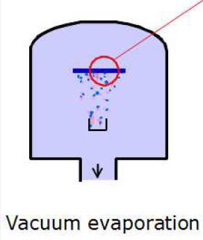
4 But first, what is ALD?

5 What can you find in the ALD Reactor?
6
7 ALD Process advantages

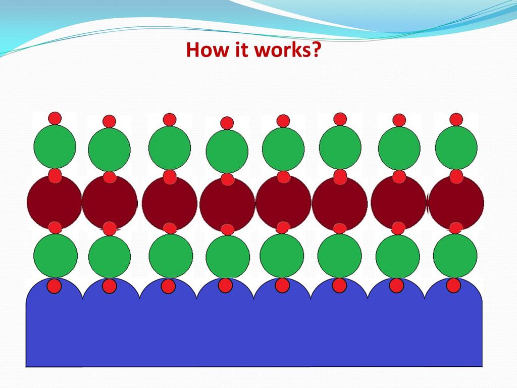
8 ALD Process working
9 1) Nanolaminate to cool down electronic devices Nano-lamination is the production of materials that are fully dense, build with atomic resolution, ultra-fine grained solids that exhibit a high concentration of interface defects. The properties of fabricated Nano laminates depend on their compositions and thicknesses.
10 Conventional CVD Methods => Source Controlled Deposition

11 Conventional Heatsink INCREASE DEVICE WEIGHT AND THICKNESS Needs adhesives.

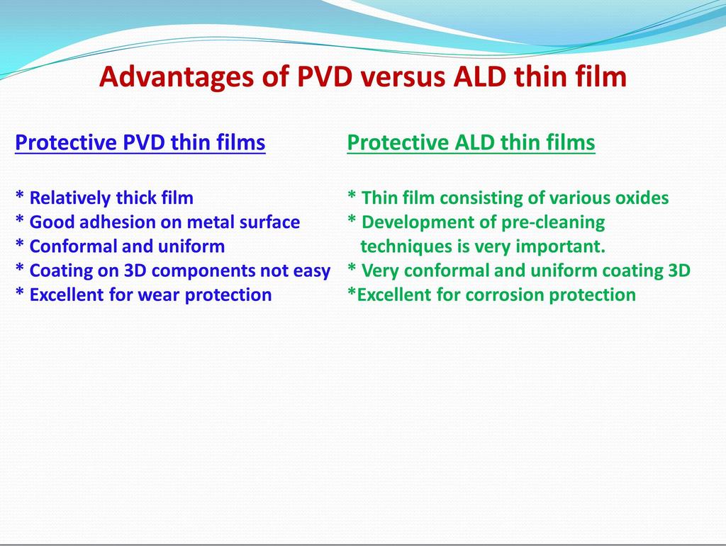
12 ALD Solution for Heatsink Surface Controlled Deposition Provide highest uniformity Precise thickness control down to nanometer level Increase the surface in contact with the heatsink thanks to the perfect atomic resolution Conformal over the smallest nanoscale features Crack defect and Pinhole free films by nature Digitally repeatable process and low process temperatures Atomic level control of film deposition : Graded / mixed/ doped layers : nanolaminates

13 Phonon superhighway principe Assumed phonon reflection pattern inside the ALD nanolaminate on the heatsink *Depend on substrate *20 C decrease in spot temperature has been shown *Enable smaller number of thermal interfaces *lighter materials with less internal thermal conductivity can be used Or * Thermal conductivity of existing materials can be made better.


14 2) ALD can also mitigate Corrosion and Tin Whisker Issues of Printed Circuit Board Assemblies Tin Whiskers grown from Pbfree solder surface Whiskers on unprotected electronics


15 Humidity External particles Liquid and gaseous impurities Heat Time Reasons for corrosions Dentrites on component & metallised holes


16 Precusors of Tin Whiskers Filament Odd Shape Eruption ( OSE)


17 Precusors of Tin Whiskers Spiral Filament Kinked Filament

18 Precusors of Tin Whiskers Hillock or Nodule
19
20
 PVD coated")


21 100Cr6 Steel in NSS tests (Neutral Salt Spray) PVD coated before the NSS test PVD coated after 2 hours in the NSS test PVD+ALD coated before the NSS test PVD+ALD coated after 670 hours in the NSS test

 COUPONS 1) Non")
 ALD treated but not")
22 3) ALD + Parylene Coating 21µm STORAGE 6 MONTHS Tin-Copper ( Sn-Cu) COUPONS 1) Non treated Sn-Cu sample 2) ALD treated but not coated
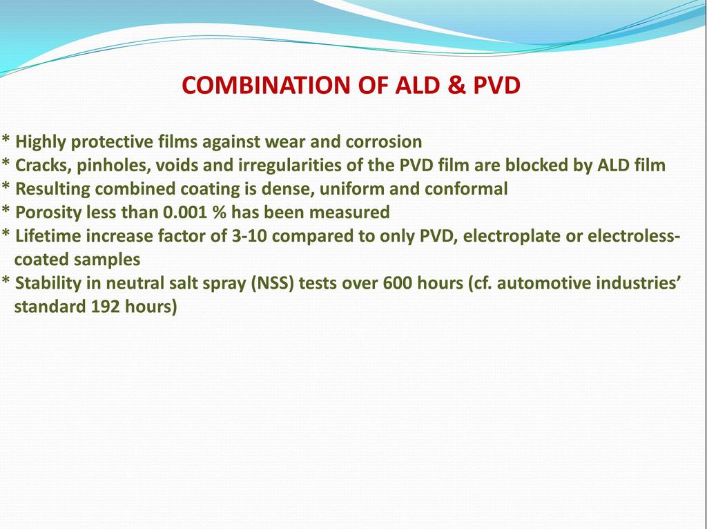
23 SUMMARY 2 With ALD process, no filament type whiskers on coupons, even for those with long time between plating and ALD coating. Shorter time ( between plating and coating) provides the good results in term of protection. Even In the coupons ALD Coated, we can observe after 6 months, whiskers, but when ALD process is mixt with Parylene coating, protection seems optimum. Coating of AL2O3 + Parylene seems today one of the best possibility to protect all electronic system working in very harsh environment, but also during the storage time. New R/D research provided recently a way to reach perfection. Due to the patent ongoing on this ALD process, we invite you to contact Microtest for further discussion and demo.
24 - ALD nano-laminate can help to cool down electronic devices in a better way than existing technologies, and also how ALD can mitigate Corrosion and Tin Whisker Issues of Printed Circuit Board Assemblies, - RTP oven can be used to heat your wafers with amazing ramp up to 250 K/s, - Probe Shield Prober in atmospheric can heat up to +300 C or cool wafers down to -65 C in order to characterize your systems, - Cryo-probers can go down to 4K or +300 C under high vacuum, to test electrically your sensors, using or not vibrations for optical measurement, - How easily produce locally on your systems or printed circuit board assemblies hot & cold in a range of C, without noise, - Device Bonder can make in situ reflow or mass reflow of C2C or C2W with high post bond accuracy,


25 3) RTP oven can be used to heat your wafers with amazing ramp up Application RTP for : Solar Wafer Annealing Crystallization and densification Low K dielectrica Solicide Formation Contact Alloying Oxidation and Nitridation III-V Ohmic allowing Implantation / Contact annealing

26 RAPID THERMAL PROCESSING PRINCIPE T Control by Thermocouple Type K 4 Max N2 for cooling process chamber


27 RTP COOLING PRINCIPE : HEAT EXCHANGER 10 KW Best system is to use cold water, C, 5 bars, from the building

28 RTP COOLING PRINCIPE : ALTERNATIVE WAYS The chiller : production of 4 KW of cold water in close loop, Remotely controlled by RTP System

29 4 Gas lines Max N2, O2, Ar, H2/N2 RTP OPTIONS Process Chamber Cooling by HE or Chiller MASSFLOW MFC Vacuum 10-3 hpa Vacuum 10-6 hpa Additional Thermocouple Process Control For T, Gas flow, Cooling, Pressure Graphite Plate SiC Coated Quartz ring 50 mm Quartz ring 75 mm Quartz ring 100 mm

30 PROGRAM EXAMPLE
31 - ALD nano-laminate can help to cool down electronic devices in a better way than existing technologies, and also how ALD can mitigate Corrosion and Tin Whisker Issues of Printed Circuit Board Assemblies, - RTP oven can be used to heat your wafers with amazing ramp up to 250 K/s, - Probe Shield Prober in atmospheric can heat up to +300 C or cool wafers down to -65 C in order to characterize your systems, - Cryo-probers can go down to 4K or +300 C under high vacuum, to test electrically your sensors, using or not vibrations for optical measurement, - How easily produce locally on your systems or printed circuit board assemblies hot & cold in a range of C, without noise, - Device Bonder can make in situ reflow or mass reflow of C2C or C2W with high post bond accuracy,
32 - 4) Probe Shield Prober in atmospheric can heat up to +300 C or cool wafers down to -65 C

33 Thermal chuck for -65 C up to 200 C Close area shielded T Controller Chiller -80 C +200 C Hygrometry control N2 Blowing Thermal Chuck in Cu
34
35


36 Probe Shield -65 C up to 200 C
37 - ALD nano-laminate can help to cool down electronic devices in a better way than existing technologies, and also how ALD can mitigate Corrosion and Tin Whisker Issues of Printed Circuit Board Assemblies, - RTP oven can be used to heat your wafers with amazing ramp up to 250 K/s, - Probe Shield Prober in atmospheric can heat up to +300 C or cool wafers down to -65 C in order to characterize your systems, - Cryo-probers can go down to 4K or +300 C under high vacuum, to test electrically your sensors, using or not vibrations for optical measurement, - How easily produce locally on your systems or printed circuit board assemblies hot & cold in a range of C, without noise, - Device Bonder can make in situ reflow or mass reflow of C2C or C2W with high post bond accuracy,

38 5) Cryo-probers can go down to 4K up to +300 C under high vacuum, to test electrically your sensors, using or not vibrations for optical measurement,

39 Backside Cryo Chamber

40 Probes Tips on Cryo Chuck


41 Cryo Chuck N2 Gas Output Liquide Nitrogen enters in

42 Cryo Chuck System

43 Cryo Chuck System

44 Cryo Chamber

45 Cryo Chamber

46 Cryo Prober

47 Cryo Prober

48 Cryo Prober installed in ENS Lab in Paris in January 2017
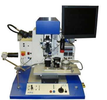
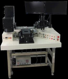
49 - ALD nano-laminate can help to cool down electronic devices in a better way than existing technologies, and also how ALD can mitigate Corrosion and Tin Whisker Issues of Printed Circuit Board Assemblies, - RTP oven can be used to heat your wafers with amazing ramp up to 250 K/s, - Probe Shield Prober in atmospheric can heat up to +300 C or cool wafers down to -65 C in order to characterize your systems, - Cryo-probers can go down to 4K or +300 C under high vacuum, to test electrically your sensors, using or not vibrations for optical measurement, - How easily produce locally on your systems or printed circuit board assemblies hot & cold in a range of C, without noise, - Device Bonder can make in situ reflow or mass reflow of C2C or C2W with high post bond accuracy,


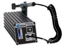
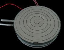
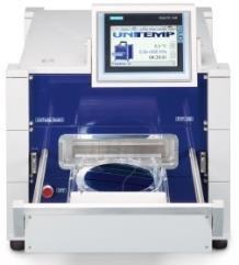
50 6) How to easily produce locally on your systems hot & cold in a range of C, without LN2, CO2, noise? FILTER + DRYER AIR CHILLER + DC INVERTER DC HEATER T PROCESS CONTROL INPUT AIR FLOW T SENSORS THERMAL CAP THERMAL HEAD


51 NEW THERMAL T TESTING FOR RAPID FAILURE ANALYSIS


52 NEW THERMAL T TESTING FOR RAPID FAILURE ANALYSIS

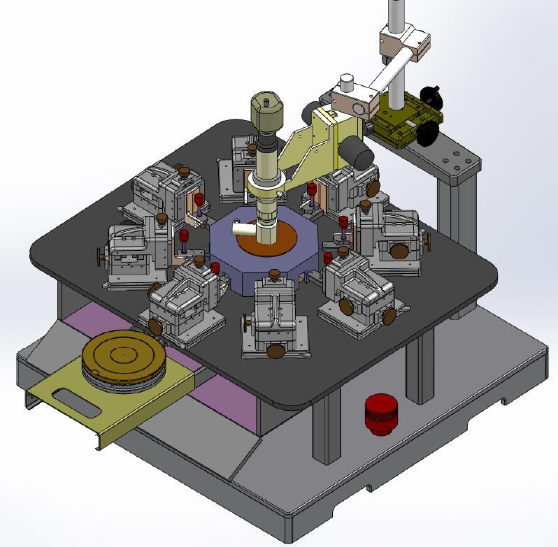
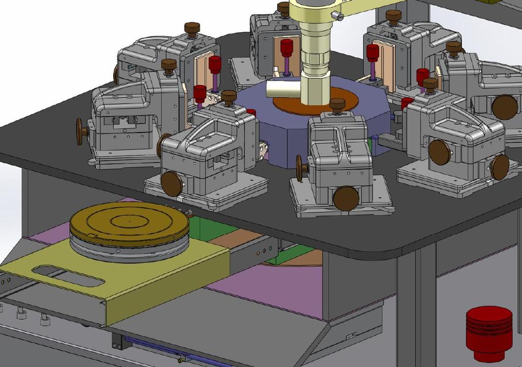
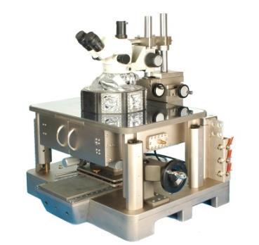
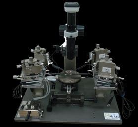
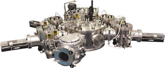
53 NEW THERMAL T TESTING ADVANTAGES Continuous Air flow up to 20 C to +225 C -55 C to 125 C / +125 C down to -125 C in less than 10 s Ultra Stable DC temperature control DC Chiller for Low audible Noise Active Control for T Profiling, Cycling, thermal shock Testing directly at application on the bench top Frost Free Operation / Built in Air Dryer No LN2 or CO2 Required and CFC Free Save 50% on electricity / Energy/ Power. Easy Roll Around wheels for Portability
54 - ALD nano-laminate can help to cool down electronic devices in a better way than existing technologies, and also how ALD can mitigate Corrosion and Tin Whisker Issues of Printed Circuit Board Assemblies, - RTP oven can be used to heat your wafers with amazing ramp up to 250 K/s, - Probe Shield Prober in atmospheric can heat up to +300 C or cool wafers down to -65 C in order to characterize your systems, - Cryo-probers can go down to 4K or +300 C under high vacuum, to test electrically your sensors, using or not vibrations for optical measurement, - How easily produce locally on your systems or printed circuit board assemblies hot & cold in a range of C, without noise, - Device Bonder can make in situ reflow or mass reflow of C2C or C2W with high post bond accuracy,
55 7)Device Bonder can make in situ reflow or mass reflow of C2C or C2W easily with high post bond accuracy, OR CHIP TO CHIP CHIP TO WAFER 55

56 LOCAL or IN SITU REFLOW PROCESS UP TO 350 C Chip Substrate UP TO 420 C Courtesy: TU Dresden
57 MASS REFLOW PROCESS CHIP Self Alignment SUBSTRATE UP TO 420 C Courtesy: TU Dresden

58 THERMO-COMPRESSION UP TO 350 C Chip Substrate UP TO 420 C Thermocompressed Au Bumps Courtesy: Alcatel


59 PRESENTATION OF BONDING MACHINE Main Camera Thermo - Bonding Arm T Controller Process Control Camera Motorized Table XY Thermo Chuck & Stamping or Deeping System ESD protection Control Panel


60 THERMAL CHUCK FOR SUBSTRATE UP TO 400 C N2 OR FORMING GAS OR FORMIC ACID VAPOR INJECTION CAPABILITIES


61 THERMAL HEATER FOR CHIP UP TO 400 C THERMAL HEATER THERMAL TOOLING

62 BONDER PP6 SPECIFICATIONS Chip sizes 100*100 µm up to 40 x 40 mm ( more in option) Substrate sizes up to 300 x 500 mm XY Table, motorized, 260 x 120 mm with 1 µm resolution Control by Joystick, direct or pulse. Bonding Force from 10 g up to 700 g Option up to 5 kg Eutectic / Thermocompression processes Ultrasonic option Flip chip capability Dispense glue or paste Scrubbing in X&Y UV light for polymerisation capability ( using flex UV light) Stamping option Dipping option Automatic Alignment with Theta control in option All process under control of PC


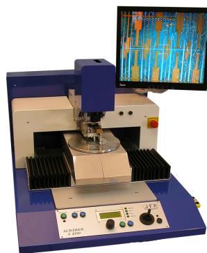
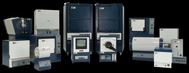


63 PROBERS DC- HF CRYO - VACUUM Thermal chuck - 65 / +300 C PRESS 12000N LITHOGRAPHY TURBO PUMP ELECTRIC SAW MICROMANIPULATORS PROBE SHIELD -65 / +300 C SUBSTRATE BONDER ALD CLUSTERS MICROTEST THANK YOU FOR YOUR ATTENTION PICK & PLACE VPO - RSO RTP - RSS TOOLS AND CONSUMABLES THERMAL CONDITIONNER -85 C up to +225 C SPIN COTATER DEVELOPER WET PROCESS SCRIBER 100 & 200 mm OVENS FURNACES INCUBATORS. EVAPORATORS
64 Guénaël RIBETTE General Manager
Lecture Day 2 Deposition
 Deposition Lecture Day 2 Deposition PVD - Physical Vapor Deposition E-beam Evaporation Thermal Evaporation (wire feed vs boat) Sputtering CVD - Chemical Vapor Deposition PECVD LPCVD MVD ALD MBE Plating
Thermal Evaporation. Theory
 Thermal Evaporation Theory 1. Introduction Procedures for depositing films are a very important set of processes since all of the layers above the surface of the wafer must be deposited. We can classify
TSV Processing and Wafer Stacking. Kathy Cook and Maggie Zoberbier, 3D Business Development
 TSV Processing and Wafer Stacking Kathy Cook and Maggie Zoberbier, 3D Business Development Outline Why 3D Integration? TSV Process Variations Lithography Process Results Stacking Technology Wafer Bonding
EV Group 300mm Wafer Bonding Technology July 16, 2008
 EV Group 300mm Wafer Bonding Technology July 16, 2008 EV Group in a Nutshell st Our philosophy Our mission in serving next generation application in semiconductor technology Equipment supplier for the
Photolithography I ( Part 2 )
") 1 Photolithography I ( Part 2 ) Chapter 13 : Semiconductor Manufacturing Technology by M. Quirk & J. Serda Bjørn-Ove Fimland, Department of Electronics and Telecommunication, Norwegian University of Science
1 Photolithography I ( Part 2 ) Chapter 13 : Semiconductor Manufacturing Technology by M. Quirk & J. Serda Bjørn-Ove Fimland, Department of Electronics and Telecommunication, Norwegian University of Science
Metallization deposition and etching. Material mainly taken from Campbell, UCCS
 Metallization deposition and etching Material mainly taken from Campbell, UCCS Application Metallization is back-end processing Metals used are aluminum and copper Mainly involves deposition and etching,
Atomic Layer Deposition
 Atomic Layer Deposition Ville Malinen R&D Engineer Nanopinnoitteita koneenrakentajille 2010 1 Introduction 1) Overview of Beneq 2) Atomic Layer Deposition (ALD), to deposit thin films, which Are dense
EE40 Lec 22. IC Fabrication Technology. Prof. Nathan Cheung 11/19/2009
 Suggested Reading EE40 Lec 22 IC Fabrication Technology Prof. Nathan Cheung 11/19/2009 300mm Fab Tour http://www-03.ibm.com/technology/manufacturing/technology_tour_300mm_foundry.html Overview of IC Technology
EQUIPMENT AND SYSTEM FOR VACUUM COATING METALLIZING, SPUTTERING, PLASMA and PECVD. Hybrid system KOLZER DGK 36
 email : carlo.gennari@fastwebnet.it web site : http://carlogennariforni.beepworld.it/kolzer.htm EQUIPMENT AND SYSTEM FOR VACUUM COATING METALLIZING, SPUTTERING, PLASMA and PECVD Hybrid system KOLZER DGK
Alternative Methods of Yttria Deposition For Semiconductor Applications. Rajan Bamola Paul Robinson
 Alternative Methods of Yttria Deposition For Semiconductor Applications Rajan Bamola Paul Robinson Origin of Productivity Losses in Etch Process Aggressive corrosive/erosive plasma used for etch Corrosion/erosion
enabling tomorrow s technologies CVD Production Systems for Industrial Coatings powered by
 enabling tomorrow s technologies CVD Production Systems for Industrial Coatings powered by www.cvdequipment.com Equipment Design, Engineering, and Manufacturing Thin film deposition systems for industrial
Welding Processes. Consumable Electrode. Non-Consumable Electrode. High Energy Beam. Fusion Welding Processes. SMAW Shielded Metal Arc Welding
 Fusion Consumable Electrode SMAW Shielded Metal Arc Welding GMAW Gas Metal Arc Welding SAW Submerged Arc Welding Non-Consumable Electrode GTAW Gas Tungsten Arc Welding PAW Plasma Arc Welding High Energy
Fabrication Technology
 Fabrication Technology By B.G.Balagangadhar Department of Electronics and Communication Ghousia College of Engineering, Ramanagaram 1 OUTLINE Introduction Why Silicon The purity of Silicon Czochralski
TSV CHIP STACKING MEETS PRODUCTIVITY
 TSV CHIP STACKING MEETS PRODUCTIVITY EUROPEAN 3D TSV SUMMIT 22-23.1.2013 GRENOBLE HANNES KOSTNER DIRECTOR R&D BESI AUSTRIA OVERVIEW Flip Chip Packaging Evolution The Simple World of C4 New Flip Chip Demands
Challenges for Embedded Device Technologies for Package Level Integration
 Challenges for Embedded Device Technologies for Package Level Integration Kevin Cannon, Steve Riches Tribus-D Ltd Guangbin Dou, Andrew Holmes Imperial College London Embedded Die Technology IMAPS-UK/NMI
KGC SCIENTIFIC Making of a Chip
 KGC SCIENTIFIC www.kgcscientific.com Making of a Chip FROM THE SAND TO THE PACKAGE, A DIAGRAM TO UNDERSTAND HOW CPU IS MADE? Sand CPU CHAIN ANALYSIS OF SEMICONDUCTOR Material for manufacturing process
BONDING OF MULTIPLE WAFERS FOR HIGH THROUGHPUT LED PRODUCTION. S. Sood and A. Wong
 10.1149/1.2982882 The Electrochemical Society BONDING OF MULTIPLE WAFERS FOR HIGH THROUGHPUT LED PRODUCTION S. Sood and A. Wong Wafer Bonder Division, SUSS MicroTec Inc., 228 SUSS Drive, Waterbury Center,
Visit
 Practical Applications for Nano- Electronics by Vimal Gopee E-mail: Vimal.gopee@npl.co.uk 10/10/12 Your Delegate Webinar Control Panel Open and close your panel Full screen view Raise hand for Q&A at the
Fluxless soldering using Electron Attachment (EA) Technology
 Technology") Fluxless soldering using Electron Attachment (EA) Technology Proprietary, patented innovation for wafer level packaging applications including wafer bump and copper pillar reflow. Air Products has partnered
Fluxless soldering using Electron Attachment (EA) Technology Proprietary, patented innovation for wafer level packaging applications including wafer bump and copper pillar reflow. Air Products has partnered
Pioneering ALD experience since The ALD Powerhouse PRODUCT CATALOGUE FOR SUNALE P-SERIES ALD SYSTEMS
 Pioneering ALD experience since 1974 The ALD Powerhouse PRODUCT CATALOGUE FOR SUNALE P-SERIES ALD SYSTEMS SUNALE P-SERIES ALD SYSTEMS PRODUCT CATALOGUE Description SUNALE P-series ALD system SUNALE P-series
Advanced Analytical Techniques for Semiconductor Assembly Materials and Processes. Jason Chou and Sze Pei Lim Indium Corporation
 Advanced Analytical Techniques for Semiconductor Assembly Materials and Processes Jason Chou and Sze Pei Lim Indium Corporation Agenda Company introduction Semiconductor assembly roadmap challenges Fine
R Sensor resistance (Ω) ρ Specific resistivity of bulk Silicon (Ω cm) d Diameter of measuring point (cm)
 ρ Specific resistivity of bulk Silicon (Ω cm) d Diameter of measuring point (cm)") 4 Silicon Temperature Sensors 4.1 Introduction The KTY temperature sensor developed by Infineon Technologies is based on the principle of the Spreading Resistance. The expression Spreading Resistance derives
4 Silicon Temperature Sensors 4.1 Introduction The KTY temperature sensor developed by Infineon Technologies is based on the principle of the Spreading Resistance. The expression Spreading Resistance derives
Fiji Thermal and Plasma Atomic Layer Deposition System (ALD) By Ultratech (Cambridge)
 By Ultratech (Cambridge)") Fiji Thermal and Plasma Atomic Layer Deposition System (ALD) By Ultratech (Cambridge) PREPARED BY: You-Sheng (Wilson) Lin, Nanolab Staff 7-30-2013 Superusers: Steve Franz You-Sheng Lin Max Ho X68923 X68923
Fiji Thermal and Plasma Atomic Layer Deposition System (ALD) By Ultratech (Cambridge) PREPARED BY: You-Sheng (Wilson) Lin, Nanolab Staff 7-30-2013 Superusers: Steve Franz You-Sheng Lin Max Ho X68923 X68923
Ultra Fine Pitch Bumping Using e-ni/au and Sn Lift-Off Processes
 Ultra Fine Pitch Bumping Using e-ni/au and Sn Lift-Off Processes Andrew Strandjord, Thorsten Teutsch, and Jing Li Pac Tech USA Packaging Technologies, Inc. Santa Clara, CA USA 95050 Thomas Oppert, and
Ultra High Barrier Coatings by PECVD
 Society of Vacuum Coaters 2014 Technical Conference Presentation Ultra High Barrier Coatings by PECVD John Madocks & Phong Ngo, General Plasma Inc., 546 E. 25 th Street, Tucson, Arizona, USA Abstract Silicon
3D technologies for integration of MEMS
 3D technologies for integration of MEMS, Fraunhofer Institute for Electronic Nano Systems Folie 1 Outlook Introduction 3D Processes Process integration Characterization Sample Applications Conclusion Folie
Surface micromachining and Process flow part 1
 Surface micromachining and Process flow part 1 Identify the basic steps of a generic surface micromachining process Identify the critical requirements needed to create a MEMS using surface micromachining
MRSI-175Ag Epoxy Dispenser
 MRSI-175Ag Epoxy Dispenser Applications: Microwave & RF Modules MEMS Semiconductor Packaging Multi-Chip Modules Hybrid Circuits Optical Modules Overview The MRSI-175Ag Conductive Epoxy Dispenser handles
LOT. Contents. Introduction to Thin Film Technology. Chair of Surface and Materials Technology
 Introduction to Thin Film Contents 1. Introduction and Application Examples (2h) 2. Preparation of Thin Films by PVD (Physical Vapor Deposition) (6h) 2.1 Vacuum Technique (1h) 2.1.1 Kinetics of Gases 2.1.2
INTRODUCTION. Think HSS
 INTRODUCTION Think HSS SUMMARY METALLURGY 2 Excellent strength 3 A super sharp edge 4 Safe and reliable tools Alloy elements 6 The influence of alloy elements 7 Standard compositions of HSS 8 The HSS-PM
Semiconductor Manufacturing Technology. IC Fabrication Process Overview
 Semiconductor Manufacturing Technology Michael Quirk & Julian Serda October 00 by Prentice Hall Chapter 9 IC Fabrication Process Overview /4 Objectives After studying the material in this chapter, you
TECHNICAL DATA SHEET 1 P a g e Revised January 9, 2014
 1 P age Revised January 9, 2014 TAIYO PSR-4000 CC01SE (UL Name: PSR-4000JV / CA-40JV) LIQUID PHOTOIMAGEABLE CURTAIN COAT SOLDER MASK Curtain Coat Application Aqueous Developing Solder Mask RoHS Compliant
Enabling Technology in Thin Wafer Dicing
 Enabling Technology in Thin Wafer Dicing Jeroen van Borkulo, Rogier Evertsen, Rene Hendriks, ALSI, platinawerf 2G, 6641TL Beuningen Netherlands Abstract Driven by IC packaging and performance requirements,
Specimen Preparation Technique for a Microstructure Analysis Using the Focused Ion Beam Process
 Specimen Preparation Technique for a Microstructure Analysis Using the Focused Ion Beam Process by Kozue Yabusaki * and Hirokazu Sasaki * In recent years the FIB technique has been widely used for specimen
Microwave Plasma Processing
 Microwave Plasma Processing MUEGGE GMBH Hochstraße 4-6 64385 Reichelsheim Fon +49 (0) 6164-93 07 11 Fax +49 (0) 6164-93 07 93 info@muegge.de www.muegge.de Microwave Plasma Processing Microwave Plasma Technology:
Reference Only. 2.Part Numbering (ex) NF Z 5B BW 2R9 L N 1 0 L
 NF Z 5B BW 2R9 L N 1 0 L") SpecNo.JENF243J-0011A-01 P1/10 CHIP NOISE FILTER NFZ5BBW LN10 REFERENCE SPECIFICATION 1.Scope This reference specification applies to NFZ5BBW_LN10L Series, Chip Noise Filter. 2.Part Numbering (ex) NF Z
SpecNo.JENF243J-0011A-01 P1/10 CHIP NOISE FILTER NFZ5BBW LN10 REFERENCE SPECIFICATION 1.Scope This reference specification applies to NFZ5BBW_LN10L Series, Chip Noise Filter. 2.Part Numbering (ex) NF Z
Lecture 12. Physical Vapor Deposition: Evaporation and Sputtering Reading: Chapter 12. ECE Dr. Alan Doolittle
 Lecture 12 Physical Vapor Deposition: Evaporation and Sputtering Reading: Chapter 12 Evaporation and Sputtering (Metalization) Evaporation For all devices, there is a need to go from semiconductor to metal.
Plasma-Enhanced Chemical Vapor Deposition
 Plasma-Enhanced Chemical Vapor Deposition Steven Glenn July 8, 2009 Thin Films Lab 4 ABSTRACT The objective of this lab was to explore lab and the Applied Materials P5000 from a different point of view.
Lab #2 Wafer Cleaning (RCA cleaning)
") Lab #2 Wafer Cleaning (RCA cleaning) RCA Cleaning System Used: Wet Bench 1, Bay1, Nanofabrication Center Chemicals Used: H 2 O : NH 4 OH : H 2 O 2 (5 : 1 : 1) H 2 O : HF (10 : 1) H 2 O : HCl : H 2 O 2
Lab #2 Wafer Cleaning (RCA cleaning) RCA Cleaning System Used: Wet Bench 1, Bay1, Nanofabrication Center Chemicals Used: H 2 O : NH 4 OH : H 2 O 2 (5 : 1 : 1) H 2 O : HF (10 : 1) H 2 O : HCl : H 2 O 2
IMRE/ETPL Flagship Project
 IMRE/ETPL Flagship Project Nanoparticulate Barrier Films & Gas Permeation Measurement Techniques for Thin Film Solar & Display Application Problems Senthil Ramadas Institute of Materials Research & Engineering
Transactions on Engineering Sciences vol 2, 1993 WIT Press, ISSN
 A study of thin-film continuous coating process by vapour deposition P. Gimondo," F. Arezzo,* B. Grifoni,* G. Jasch& "Centra Sviluppo Materiali SpA, Via di Castel & Von Ardenne Anlagentchnik GmbH, Plattleite
Vacuum Arc Remelting (VAR)
") ALD Vacuum Technologies High Tech is our Business Vacuum Arc Remelting (VAR) Vacuum Arc Remelting Processes and Furnaces VAR Vacuum Arc Remelting (VAR) ALD is one of the leading suppliers of vacuum melting
ALD Vacuum Technologies High Tech is our Business Vacuum Arc Remelting (VAR) Vacuum Arc Remelting Processes and Furnaces VAR Vacuum Arc Remelting (VAR) ALD is one of the leading suppliers of vacuum melting
Dr. Priyabrat Dash Office: BM-406, Mob: Webpage: MB: 205
 Email: dashp@nitrkl.ac.in Office: BM-406, Mob: 8895121141 Webpage: http://homepage.usask.ca/~prd822/ MB: 205 Nonmanufacturing In continuation from last class... 2 Top-Down methods Mechanical-energy methods
Cutting Tool Materials and Cutting Fluids. Dr. Mohammad Abuhaiba
 Cutting Tool Materials and Cutting Fluids HomeWork #2 22.37 obtain data on the thermal properties of various commonly used cutting fluids. Identify those which are basically effective coolants and those
THIN IMMERSION TIN USING ORGANIC METALS
 THIN IMMERSION TIN USING ORGANIC METALS Jim Kenny, Nils Arendt, Bernhard Wessling, and Karl Wengenroth Enthone Inc., A Business of Cookson Electronics West Haven, CT, USA ABSTRACT With the international
RoHS Compliance Document
 D2-Pak RoHS Compliance Document Contents: 1. 2. Solder Reflow 3. Tin Whisker Report D2-pak (3 or 5 Lead) BOM 1 90598-46-2 0.05808 11% 3.8% Lead Frame Copper 0.94840 Die Attach Soft Solder 0.01200 Cu 7440-50-8
Atomic Layer Deposition(ALD)
") Atomic Layer Deposition(ALD) AlO x for diffusion barriers OLED displays http://en.wikipedia.org/wiki/atomic_layer_deposition#/media/file:ald_schematics.jpg Lam s market-leading ALTUS systems combine CVD
Atomic Layer Deposition(ALD) AlO x for diffusion barriers OLED displays http://en.wikipedia.org/wiki/atomic_layer_deposition#/media/file:ald_schematics.jpg Lam s market-leading ALTUS systems combine CVD
Atomic Oxygen-Resistant, Static-Dissipative, Pinhole-Free Coatings for Spacecraft
 Physical Sciences Inc. VG10-109 Atomic Oxygen-Resistant, Static-Dissipative, Pinhole-Free Coatings for Spacecraft Michelle T. Schulberg, Robert H. Krech, Frederick S. Lauten Physical Sciences Inc. Roy
Supporting Information
 Supporting Information Fast-Response, Sensitivitive and Low-Powered Chemosensors by Fusing Nanostructured Porous Thin Film and IDEs-Microheater Chip Zhengfei Dai,, Lei Xu,#,, Guotao Duan *,, Tie Li *,,
Hot Pin Pull Method New Test Procedure for the Adhesion Measurement for 3D-MID
 Hot Pin Pull Method New Test Procedure for the Adhesion Measurement for 3D-MID HARTING Mitronics Christian Goth in cooperation with: FAPS Thomas Kuhn, Gerald Gion, Jörg Franke 11 th International Congress
Basic PCB Level Assembly Process Methodology for 3D Package-on-Package
 Basic PCB Level Assembly Process Methodology for 3D Package-on-Package Vern Solberg STC-Madison Madison, Wisconsin USA Abstract The motivation for developing higher density IC packaging continues to be
Keeping Cool!: selecting high performance thermal materials for LED Lighting applications. Ian Loader 25/03/14
 Keeping Cool!: selecting high performance thermal materials for LED Lighting applications Ian Loader 25/03/14 1 Target Points to cover Basics of Thermal Management Considerations for thermal materials
Reference Only. Spec. No. JENF243E-0003Q-01 P 1 / 8. Chip EMIFIL LC Combined Type for Large Current NFE61PT 1H9 Reference Specification
 Spec. No. JENF243E-0003Q-01 P 1 / 8 Chip EMIFIL LC Combined Type for Large Current NFE61PT 1H9 Reference Specification 1. Scope This reference specification applies to Chip EMIFIL LC Combined Type for
UTILIZATION OF ATMOSPHERIC PLASMA SURFACE PREPARATION TO IMPROVE COPPER PLATING PROCESSES.
 SESSION 14 MATERIALS AND PROCESSES FOR ADVANCED PACKAGING UTILIZATION OF ATMOSPHERIC PLASMA SURFACE PREPARATION TO IMPROVE COPPER PLATING PROCESSES. Eric Schulte 1, Gilbert Lecarpentier 2 SETNA Corporation
C27200 CuZn37 Industrial Rolled
 C272 Alloy Designation EN DIN CEN/TS 13388 (2.321) CW58L JIS C 272 BS CZ 17 UNS C272 Brass Rolled Products KME offers a wide range of brass rolled products in the form of strips, sheets and discs in order
WF6317. A superactive low-volatile/high heat-resistant water-soluble flux for ball soldering
 WF637 A superactive low-volatile/high heat-resistant water-soluble flux for ball soldering Low viscosity and high tacking power stabilize ball holding force and ensures excellent solder wettability Easy
Vacuum deposition of TiN
 J.Lorkiewicz DESY.27.10.02 Vacuum deposition of TiN (TiN coating of high power coupler elements as an anti-multipactor remedy at DESY) The scope of the project: - reducing secondary electron emission and
Journal of Chemical and Pharmaceutical Research, 2017, 9(1): Research Article
: Research Article") Available online www.jocpr.com Journal of Chemical and Pharmaceutical Research, 2017, 9(1):163-167 Research Article ISSN : 0975-7384 CODEN(USA) : JCPRC5 Synthesis and Characterization of Carbon Nano Spheres
Available online www.jocpr.com Journal of Chemical and Pharmaceutical Research, 2017, 9(1):163-167 Research Article ISSN : 0975-7384 CODEN(USA) : JCPRC5 Synthesis and Characterization of Carbon Nano Spheres
Ultralow Residue Semiconductor Grade Fluxes for Copper Pillar Flip-Chip
 Ultralow Residue Semiconductor Grade Fluxes for Copper Pillar Flip-Chip SzePei Lim (Presenter), Jason Chou, Maria Durham, and Dr. Andy Mackie Indium Corporation 1 Outline of Presentation Roadmaps and challenges
Surface Micromachining
 Surface Micromachining Outline Introduction Material often used in surface micromachining Material selection criteria in surface micromachining Case study: Fabrication of electrostatic motor Major issues
Semiconductor Technology
 Semiconductor Technology von A bis Z Metallization www.halbleiter.org Contents Contents List of Figures List of Tables II III 1 Metallization 1 1.1 Requirements on metallization........................
Hot-Dip Galvanized Fabrication Considerations
 Hot-Dip Galvanized Fabrication Considerations TECHNICAL BULLETIN JANUARY 27, 2016 Forming Hot-dip galvanized sheet can be formed almost as readily as uncoated cold rolled sheet. It can be formed in a variety
IMPACT OF LEAD-FREE COMPONENTS AND TECHNOLOGY SCALING FOR HIGH RELIABILITY APPLICATIONS
 IMPACT OF LEAD-FREE COMPONENTS AND TECHNOLOGY SCALING FOR HIGH RELIABILITY APPLICATIONS Chris Bailey, Ph.D. University of Greenwich London, United Kingdom c.bailey@gre.ac.uk ABSTRACT Semiconductor technology
Photonic Drying Pulsed Light as a low Temperature Sintering Process
 Photonic Drying Pulsed Light as a low Temperature Sintering Process Lou Panico Xenon Corporation W E S T E R N M I C H I G A N U N I V E R S I T Y PRESENTATION OVERVIEW What is Printed Electronics Materials
Industrial Diamonds: Present and the Future
 M.Sc Miroljub Vilotijevic Dr. Borislav Dacic Industrial Diamonds: Present and the Future Three resorting qualities of diamond available today for industrial use are: natural diamond (i), synthetic diamond
Development of an Low Cost Wafer Level Flip Chip Assembly Process for High Brightness LEDs Using the AuSn Metallurgy
 Development of an Low Cost Wafer Level Flip Chip Assembly Process for High Brightness LEDs Using the AuSn Metallurgy Gordon Elger, Rafael Jordan, Maria v. Suchodoletz and Hermann Oppermann Fraunhofer Institute
CVD DIAMOND AND RELATED MATERIALS AT INSTITUTE FOR SPACE RESEARCH AND INDUSTRY: RESEARCH, DEVELOPMENT AND INNOVATION.
 CVD DIAMOND AND RELATED MATERIALS AT INSTITUTE FOR SPACE RESEARCH AND INDUSTRY: RESEARCH, DEVELOPMENT AND INNOVATION. VLADIMIR JESUS TRAVA-AIROLDI Instituto Nacional de Pesquisas Espaciais-INPE São José
Chips Face-up Panelization Approach For Fan-out Packaging
 Chips Face-up Panelization Approach For Fan-out Packaging Oct. 15, 2015 B. Rogers, D. Sanchez, C. Bishop, C. Sandstrom, C. Scanlan, TOlson T. REV A Background on FOWLP Fan-Out Wafer Level Packaging o Chips
NanoSystemsEngineering: NanoNose Final Status, March 2011
 1 NanoSystemsEngineering: NanoNose Final Status, March 2011 The Nanonose project is based on four research projects (VCSELs, 3D nanolithography, coatings and system integration). Below, the major achievements
Etching Mask Properties of Diamond-Like Carbon Films
 N. New Nawachi Diamond et al. and Frontier Carbon Technology 13 Vol. 15, No. 1 2005 MYU Tokyo NDFCT 470 Etching Mask Properties of Diamond-Like Carbon Films Norio Nawachi *, Akira Yamamoto, Takahiro Tsutsumoto
Ajay Kumar Gautam [VLSI TECHNOLOGY] VLSI Technology for 3RD Year ECE/EEE Uttarakhand Technical University
![Ajay Kumar Gautam [VLSI TECHNOLOGY] VLSI Technology for 3RD Year ECE/EEE Uttarakhand Technical University](/thumbs/75/72824557.jpg "Ajay Kumar Gautam [VLSI TECHNOLOGY] VLSI Technology for 3RD Year ECE/EEE Uttarakhand Technical University") 2014 Ajay Kumar Gautam [VLSI TECHNOLOGY] VLSI Technology for 3RD Year ECE/EEE Uttarakhand Technical University Page1 Syllabus UNIT 1 Introduction to VLSI Technology: Classification of ICs, Scale of integration,
2014 Ajay Kumar Gautam [VLSI TECHNOLOGY] VLSI Technology for 3RD Year ECE/EEE Uttarakhand Technical University Page1 Syllabus UNIT 1 Introduction to VLSI Technology: Classification of ICs, Scale of integration,
HOT-DIP TINNED COPPER AND COPPER ALLOY STRIP
 HOT-DIP TINNED COPPER AND COPPER ALLOY STRIP HOT-DIP TINNED STRIP WHY HOT DIP TINNING? Characteristic for hot-dip tinned coatings is the formation of an intermetallic phase (IMP) between the base material
Reference Only. Spec. No. JENF243E-0002Q-01 P1 / 8
 Spec. No. JENF243E-0002Q-01 P1 / 8 Chip EMIFIL LC Combined Type for Large Current NFE31PT 1E9 Reference Specification 1. Scope This reference specification applies to Chip EMIFIL LC Combined Type for Large
Reference Only. Spec. No. JENF243D-0006K-01 P 1/ 8
 Spec. No. JENF243D-0006K-01 P 1/ 8 Chip EMIFIL LC Combined Monolithic NFL21SP X1C Reference Specification 1. Scope This reference specification applies to Chip EMIFIL LC Combined Monolithic Type NFL21S
Thin Wafers Bonding & Processing
 Thin Wafers Bonding & Processing A market perspective 2012 Why New Handling Technologies Consumer electronics is today a big driver for smaller, higher performing & lower cost device configurations. These
Low temperature deposition of thin passivation layers by plasma ALD
 1 Low temperature deposition of thin passivation layers by plasma ALD Bernd Gruska, SENTECH Instruments GmbH, Germany 1. SENTECH in brief 2. Low temperature deposition processes 3. SENTECH SI ALD LL System
Lead-Free Solder Bump Technologies for Flip-Chip Packaging Applications
 Lead-Free Solder Bump Technologies for Flip-Chip Packaging Applications Zaheed S. Karim 1 and Jim Martin 2 1 Advanced Interconnect Technology Ltd. 1901 Sunley Centre, 9 Wing Yin Street, Tsuen Wan, Hong
New Technology for High-Density LSI Mounting in Consumer Products
 New Technology for High-Density Mounting in Consumer Products V Hidehiko Kira V Akira Takashima V Yukio Ozaki (Manuscript received May 29, 2006) The ongoing trend toward downsizing and the growing sophistication
Figure 2.3 (cont., p. 60) (e) Block diagram of Pentium 4 processor with 42 million transistors (2000). [Courtesy Intel Corporation.
 (e) Block diagram of Pentium 4 processor with 42 million transistors (2000). [Courtesy Intel Corporation.") Figure 2.1 (p. 58) Basic fabrication steps in the silicon planar process: (a) oxide formation, (b) selective oxide removal, (c) deposition of dopant atoms on wafer, (d) diffusion of dopant atoms into exposed
Figure 2.1 (p. 58) Basic fabrication steps in the silicon planar process: (a) oxide formation, (b) selective oxide removal, (c) deposition of dopant atoms on wafer, (d) diffusion of dopant atoms into exposed
Lecture 19 Microfabrication 4/1/03 Prof. Andy Neureuther
 EECS 40 Spring 2003 Lecture 19 Microfabrication 4/1/03 Prof. ndy Neureuther How are Integrated Circuits made? Silicon wafers Oxide formation by growth or deposition Other films Pattern transfer by lithography
Modern Methods of Surface Engineering
 LVIV POLYTECHNIC NATIONAL UNIVERSITY Modern Methods of Surface Engineering Institute of Engineering Mechanics and Transport Department of Applied Materials Science and Materials Engineering Asssistant
SUPRA 50 - SP 510. Fe-Ni SOFT MAGNETIC ALLOYS
 I. INTRODUCTION SUPRA 50 - SP 510 Fe-Ni SOFT MAGNETIC ALLOYS The Imphy Alloys range of soft magnetic alloys based on the 50% nickel composition includes the following grades : - SUPRA 50 / SUPRA 50 SP
Vacuum Furnaces Furnaces for Advanced Materials
 Vacuum Furnaces Furnaces for Advanced Materials Vacuum Furnaces and Furnaces for Advanced Materials IHI is one of the largest furnace manufacturers in the following industries. AUTOMOTIVE AEROSPACE TOOL
Leadership in Soft Magnetic Alloys
 Leadership in Soft Magnetic Alloys Carpenter Technology Corporation offers a wide selection of soft magnetic alloys to meet your material specifications. Choose from high permeability alloys, shielding
Recent Advances in Die Attach Film
 Recent Advances in Die Attach Film Frederick Lo, Maurice Leblon, Richard Amigh, and Kevin Chung. AI Technology, Inc. 70 Washington Road, Princeton Junction, NJ 08550 www.aitechnology.com Abstract: The
Liquid Accelerated Cold Spray
 Liquid Accelerated Cold Spray CSAT Meeting Presentation 10/30/12 PI: Tom Butler, Ormond, LLC 253-852-1298 TPOC: Victor Champagne, ARL Phase II SBIR Contract # W911QX-11-C-0002 1 Presentation Summary Introduction
ALD and CVD of Copper-Based Metallization for. Microelectronic Fabrication. Department of Chemistry and Chemical Biology
 ALD and CVD of Copper-Based Metallization for Microelectronic Fabrication Yeung Au, Youbo Lin, Hoon Kim, Zhengwen Li, and Roy G. Gordon Department of Chemistry and Chemical Biology Harvard University Introduction
Dilatometer L 76 L 75 Horizontal L 75 Vertical
 Dilatometer L 76 L 75 Horizontal L 75 Vertical General Dilatometry is a technique which measures the dimensional change of a substance as a function of temperature while the substance is subjected to a
ALD Vacuum Technologies High Tech is our Business. DualTherm. Double Chamber Vacuum Furnace for flexible heat treatment
 ALD Vacuum Technologies High Tech is our Business Double Chamber Vacuum Furnace for flexible heat treatment High Tech is our Business ALD is a brand name associated world-wide with innovative vacuum technology
Isolation Technology. Dr. Lynn Fuller
 ROCHESTER INSTITUTE OF TECHNOLOGY MICROELECTRONIC ENGINEERING Isolation Technology Dr. Lynn Fuller Motorola Professor 82 Lomb Memorial Drive Rochester, NY 14623-5604 Tel (585) 475-2035 Fax (585) 475-5041
An Innovative High Throughput Thermal Compression Bonding Process
 An Innovative High Throughput Thermal Compression Bonding Process Li Ming 2 September 2015 Outline Introduction Throughput improved TCB Process Liquid Phase Contact (LPC) bonding Flux-LPC-TCB under inert
High Performance Alloys. Characteristics
 Alloy Designation EN DIN CEN/TS 13388 UNS High Performance Alloys Chemical Composition Weight percentage We have developed a wide range of high performance alloys with excellent properties regarding conductivity,
Analyzing & Testing. Guarded Hot Plate - GHP. Method, Instrumentation, Applications. GHP 456 Titan. Leading Thermal Analysis
 Analyzing & Testing Guarded Hot Plate - GHP Method, Instrumentation, Applications GHP 456 Titan Leading Thermal Analysis GHP 456 Titan - Guarded Hot Plate System GHP 456 Titan - Principle of Operation
Becoming Lead Free. Automotive Electronics. Antonio Aires Soldering Technical Specialist Visteon Corporation - Palmela Plant
 Automotive Electronics Becoming Lead Free Antonio Aires Soldering Technical Specialist Visteon Corporation - Palmela Plant 1 Agenda 1. Leadfree Electronics Drivers 2. Requirements 3. Areas of Impact 4.
Optical Coatings. Photonics 4 Luxury Coatings , Genève. Dr. Andreas Bächli Head of Optical Coatings at RhySearch, Buchs (SG)
") Optical Coatings Photonics 4 Luxury Coatings 21.06.2017, Genève Dr. Andreas Bächli Head of Optical Coatings at RhySearch, Buchs (SG) RhySearch The Research- and Innovation Center in the Rhine Valley RhySearch
Optical Coatings Photonics 4 Luxury Coatings 21.06.2017, Genève Dr. Andreas Bächli Head of Optical Coatings at RhySearch, Buchs (SG) RhySearch The Research- and Innovation Center in the Rhine Valley RhySearch
Mold Design. 12. Mold Materials. Bong-Kee Lee School of Mechanical Engineering Chonnam National University
 12. Mold Materials Bong-Kee Lee Chonnam National University Mold Materials easy toolmaking good performance during production good machining properties ease of hear treatment where hardening is required
The Effects of Defects on the Moisture-Barrier Performance of Clear Coatings on Polymer Substrates.
 AIMCAL, CHARLESTON, SC, 2013 The Effects of Defects on the Moisture-Barrier Performance of Clear Coatings on Polymer Substrates. The National Centre for Printed Electronics ALF part SMITH of Centre for
PROCESSING OF INTEGRATED CIRCUITS
 PROCESSING OF INTEGRATED CIRCUITS Overview of IC Processing (Part I) Silicon Processing Lithography Layer Processes Use in IC Fabrication (Part II) Integrating the Fabrication Steps IC Packaging (Part
AC : MICROWAVE PLASMA CLEANER DESIGN FOR SEMI- CONDUCTOR FABRICATION AND MATERIALS PROCESSING LABO- RATORY USE
 AC 2011-2416: MICROWAVE PLASMA CLEANER DESIGN FOR SEMI- CONDUCTOR FABRICATION AND MATERIALS PROCESSING LABO- RATORY USE Mustafa G. Guvench, University of Southern Maine Mustafa G. Guvench received M.S.