Copper Wire Packaging Reliability for Automotive and High Voltage
|
|
|
- Cecilia Pitts
- 6 years ago
- Views:
Transcription
1 Copper Wire Packaging Reliability for Automotive and High Voltage Tu Anh Tran AMPG Package Technology Manager Aug TM External Use
2 Agenda New Automotive Environments Wire Bond Interconnect Selection Challenge in High Temperature Bake Challenge in Temperature Cycling Challenge in Moisture and High Voltage Testing Freescale Copper Wire Strategy and Progress Summary External Use 1

3 New Automotive Environments External Use 2
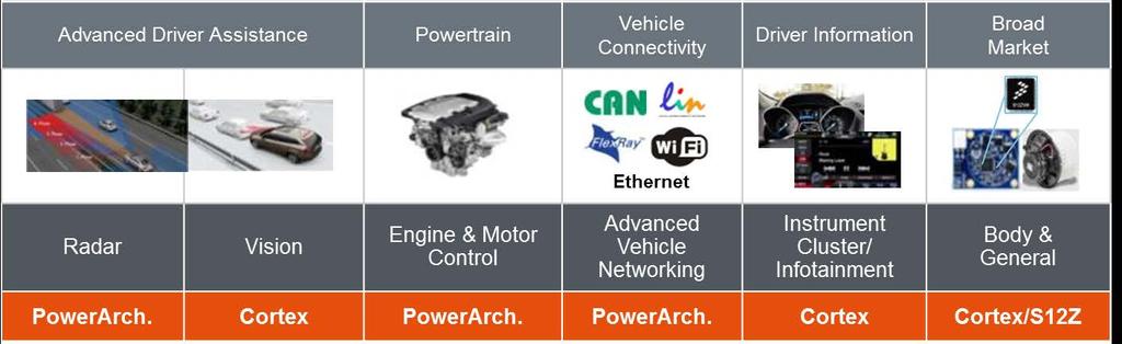


4 Automotive Microcontrollers Product Portfolio External Use 3

")

5 More Challenging Powertrain Applications Previous Under the Hood Application Profile Junction Temperature (ºC) Duration (hours) 135 1, ,600 Total 6,000 New Under the Hood Application Profile Junction Temperature (ºC) Duration (hours) 150 3, , ,000 Total 20,000 External Use 4
6 Reaching for a Higher Packaging Certification Level Certify next-generation multicore automotive controller packages (BGA and Leadframe) to AEC Grade 0, 2X AEC Grade 1. Package Stress AEC Grade 1 AEC Grade 0 Air-to-air Temperature Cycling AATC (-50/150ºC) 1000 cycles 2000 cycles High Temp Bake HTB-150ºC 1000 hours 2000 hours High Temp Bake HTB-175ºC 500 hours 1000 hours Unbiased HAST-110ºC Biased HAST-110ºC or THB (85ºC / 85%RH) 264 hours 264 hour HAST or 1008 hour THB External Use 5

7 Presentation Focus Areas D BGA and LQFP Cross Sections E D E C B A A B C F Packaging Materials A B C D E F Silicon Die Die Attach Substrate / Leadframe Wire Epoxy Mold Compound Solder Sphere Cu Ball Bond Reliability Focused Areas Cu Wire Bond Compatibility and High Voltage External Use 6
8 Wire Bond Interconnect Selection External Use 7
 Over Pad Metallization Pd-Cu Wire on Al Pad Passing at")

9 High Reliability Wire Bond Interconnect Wire Bond Interconnect Options Al Pad Au Wire on Al Pad Failing at 1008hr HTB-175 C Au Wire Cu Wire Pd-Cu Wire Al Pad + Ni / Pd / (Au) Over Pad Metallization Pd-Cu Wire on Al Pad Passing at 1008hr HTB-175 C Au Wire Cu Wire Pd-Cu Wire Excessive intermetallic compound (IMC) growth leading to Kirkendall voiding and electrical failure Minimal IMC growth Freescale selected Pd-Cu wire on Al interconnect for AEC Grade 0. External Use 8
 vs.")

10 Optimizing Pd Coverage for Pd-Cu Ball Bonds Pd Coverage on Free Air Balls (FAB) vs. EFO Current for 3 Pd-Cu Wire Types Pd Coverage on Etched Ball Bonds vs. EFO Current for 3 Pd-Cu Wire Types Pd-Cu wire B has best Pd coverage and widest EFO current window. External Use 9

 EFO Current")


11 Pd-Cu Wire Can Fail HAST with Improper Pd Coverage Incorrect (High) EFO Current Optimized (Low) EFO Current Corrosion Layer Corrosion Layer Failed 96 hour HAST-130 C due to Cu-Al IMC Corrosion Passed 192 hour HAST-130 C External Use 10
12 High Temperature Bake Challenges External Use 11

 Barrier Layer Cu")
 Cu-Al")

13 Cu Wire Pull Failure Modes in High Temperature Bake Wire Break (Preferred) Pad Lift (Exposing Barrier or Cu BEOL) Barrier Layer Cu BEOL Ball Lift Exposing Intermetallic Compound (IMC) Cu-Al IMC Cu-Al IMC Wire Pull Failure Mode Preference: Wire Break > Pad Lift >> Ball Lift External Use 12
. Rate of pad lifts reduced with higher EFO current for Pd-Cu wire.")
14 High Temperature Bake Performance Decap / Wire Pull Failure Mode Distribution For Pd-Cu Wire at Different EFO Currents and Bare Cu Wire (Control) 2016 hours/150ºc is not equivalent to 1008 hours/175ºc (AEC G0). Rate of pad lifts reduced with higher EFO current for Pd-Cu wire. External Use 13

15 Intermetallic Compound (IMC) Growth and Peripheral Interfacial Crack Intermetallic Formation Reaction Rate K (cm 2 /sec) Temperature (150 C) Au - Al 110 X Cu - Al 3.18 X PdCu - Al 2.89 X Thicker Cu-Al IMC found on bare Cu. Longer peripheral interfacial crack above Cu-Al IMC found on bare Cu. Interfacial crack resulted in pad lifts or ball lifts in bare Cu. Pd-Cu wire: Regress IMC formation and delay interfacial crack growth. External Use 14

16 Cu Ball Voiding Found in Pd-Cu Wire 2016 hour HTB-150 C 2016 hour HTB-175 C Cu Voiding Cu voiding found only with Pd-Cu wire at high bake temperature 175 C and contributed to pad lifting during wire pull. External Use 15


17 Cu Voiding in Pd-Cu Ball Investigation Cu Voiding Spot 1 Cu, Al, Si, S, O, C Cu voiding decreased with increasing EFO current. Sulfur detected in Cu voiding areas. No Cl or S detected in Cu-Al IMC. Spot 4 Cu, Al, Si, S, O, C External Use 16
18 Cu Voiding in Pd-Cu Ball Mechanism Chamfer Squeeze e ē - e-e- e-e- Cu (Anode) Cu Cu + + e Cu Cu ē - e ē - e-e- e ē - e-e- Low EFO Current (Less Cu Exposure) Pd (Cathode) Examples: O 2 + H 2 O > 4OH - 2H H 2 e- High EFO Current (More Cu Exposure) After encapsulation, moisture absorbed by the mold compound can cause ions to become mobile, creating a galvanic cell between the Pd and Cu. When the Anode (oxidizing metal) area is much smaller than the Cathode (noble metal), the corrosion rate is accelerated. We propose that the driving force of this galvanic corrosion is related to Sulfur concentration present in mold compound in HTB-175C. External Use 17


19 Reducing Cu Voiding in Pd-Cu Balls 504 HTB-175ºC 1008 HTB-175ºC 2016 HTB-175ºC Molding Compound SO 4 = : X PPM Cu Voiding Molding Compound SO 4 = : 0.25X PPM Reducing Cu voiding in Pd-Cu ball can be achieved by lowering sulfate (adhesion promoter) in mold compound. However, Cu voiding shows no reliability risk. Packages passed electrical test at 2016 HTB-175C (2X AEC-G0). External Use 18
20 Temperature Cycling Challenges External Use 19


21 Achieving No Wire-Pull Ball-Lift Failures After Temperature Cycling Al and underlying barrier layer 2000 Cycles of Temperature Cycling Ball Lift Ball lift after decap / wire pull at 2000 AATC cycles observed on both bare Cu and Pd-Cu wires on Al pad. Crack in Al pad caused ball lift during wire pull. Assembly process optimized to eliminate ball lift issue after Temperature Cycling. Crack at Ball Edge Before Optimization Cohesive Crack in Al Pd-Cu Ball After External Use 20


22 Exceeding AEC Grade 0 Requirement Wire Pull (gf) Ball Shear (gf) JEDEC LSL = 1.8gf for 20um wire LSL = 2gf for 43um ball diameter Passed electrical test at 2X AEC Grade 0. Passed decap / wire pull and ball shear at 2X AEC Grade 0 with no ball lifts. External Use 21
23 Moisture and High Voltage Challenges External Use 22
24 Cu-Al Intermetallic Compound Corrosion in HAST / THB Issues Initial Optimized Resolutions Cu-Al Intermetallic (IMC) bond layer corrosion (biased HAST failure) Al Corrosion crack Cu Cu Solid IMC Al Wire bond process optimization Internal testing demonstrates higher ph and lower Cl - are best for CuWB reliability. FSL specifies ph and Cl - FSL tightened MC specification for Au wire to meet CuWB requirement Chloride (Cl-), principally from mold compound, can cause corrosion at the Cu ball to IMC interface resulting in open circuits. Goal to use same BOM for CuWB and AuWB, including molding compound (MC). Internal research developed methods to determine acceptable ph and Cllevels within ranges specified by suppliers. Specs often renegotiated with suppliers to allow same MC used for AuWB. Universal ph and Cl- level spec with reasonable values is not possible. Acceptable ph and Cl- levels vary among MCs due to other MC attributes. Acceptable ph and Cl- levels vary with voltage. External Use 23

25 Mold Compound Studies for Cu Wire HAST Compatibility 98 Biased HAST Studies with 19 Mold Compounds across 5 Assembly Sites Low Medium High 3V 3V 5V Pass 3V Pass 3V 5V 14V 14V Pass 5V Pass 3V Pass 5V Fails Pass 65V 65V Pas s Fail Pass 5V Pass 3V Low Medium High ph and Cl- specs are not constant, and are unique for each MC. Probability of Cu-Al bias HAST corrosion increases with bias voltage. External Use 24
26 Freescale Copper Wire Strategy and Progress External Use 25
 Focus: Non-automotive conversions Non-automotive production 2012: First automotive conversion Focus: 2 internal and 1 external factories")
27 Freescale Strategy: Migrating to Fine Gauge Cu Wires Cu wire bond technology Intellectual Property: > 40 USA patent applications filed > 60 conference presentations and publications since : Strategy: All NPI with Cu wire (except Sensors) Focus: Non-automotive conversions Non-automotive production 2012: First automotive conversion Focus: 2 internal and 1 external factories First AEC grade 3 production 2013: First automotive production : Convert entire portfolio to Cu wire 1 Billion units shipped in April 15 Focus: 2 internal and 5 external factories >1200 qualifications completed (418 auto / analog quals) Sensor qualifications started Scope: 17 wafer technologies, 6 wafer fabs, 7 assembly sites 7 package platforms: Lead frame and Substrate Bare Cu and Pd-Cu wires External Use 26

28 General Production Status Update Production Metrics: Cumulative Volume: > 1 Billion across 2 internal and 5 external sites Automotive: 30%, Consumer/Industrial: 70% Internal Volume Shipment Mix: > 50% with Cu wire Quality Incidents: 0.02 ppm Qualifications: 98% of the portfolio qualified Reliability Tiers: Consumer, Industrial, AEC grade 1 and 0 Freescale Cumulative Cu Wire Volumes External Use 27
29 Summary External Use 28
30 Summary The requirement for next-generation powertrain product packaging is AEC Grade 0 which is 2X the current requirement. Freescale package is a cost-effective solution using Pd-Cu wire on Aluminum bond pad meeting and exceeding the challenging AEC Grade 0 packaging reliability requirement. Mold compounds were studied and reformulated to accommodate high voltage up to 65 V. FSL successfully launched fine gauge Cu wire production to the market including automotive. External Use 29
31 Freescale Semiconductor, Inc. External Use
MATERIAL NEEDS AND RELIABILITY CHALLENGES IN AUTOMOTIVE PACKAGING UNDER HARSH CONDITIONS
 MATERIAL NEEDS AND RELIABILITY CHALLENGES IN AUTOMOTIVE PACKAGING UNDER HARSH CONDITIONS Varughese Mathew NXP Semiconductors 6501 William Cannon Drive, Austin TX, USA Automotive Innovation Driven by Electronics
Copper Wire Bonding: the Last Frontier of Cost Savings. Bernd K Appelt Business Development ASE (U.S.) Inc. April 11, 2012
 Inc. April 11, 2012") Copper Wire Bonding: the Last Frontier of Cost Savings Bernd K Appelt Business Development ASE (U.S.) Inc. April 11, 2012 Outline Introduction Fundamental Study Reliability Study Monitoring Data High Volume
Copper Wire Bonding: the Last Frontier of Cost Savings Bernd K Appelt Business Development ASE (U.S.) Inc. April 11, 2012 Outline Introduction Fundamental Study Reliability Study Monitoring Data High Volume
WorkShop Audace. INSA ROUEN 8 juin 2012
 WorkShop Audace INSA ROUEN 8 juin 2012 Global Standards for the Microelectronics Industry JEDEC standards for product level qualification Christian Gautier Content JEDEC overview Environmental reliability
Quality and Reliability Report
 Quality and Reliability Report Product Qualification MASW-007921 2mm 8-Lead Plastic Package QTR-0148 M/A-COM Technology Solutions Inc. 100 Chelmsford Street Lowell, MA 01851 Tel: (978) 656-2500 Fax: (978)
Failure Modes in Wire bonded and Flip Chip Packages
 Failure Modes in Wire bonded and Flip Chip Packages Mumtaz Y. Bora Peregrine Semiconductor San Diego, Ca. 92121 mbora@psemi.com Abstract The growth of portable and wireless products is driving the miniaturization
HBLED packaging is becoming one of the new, high
 Ag plating in HBLED packaging improves reflectivity and lowers costs JONATHAN HARRIS, President, CMC Laboratories, Inc., Tempe, AZ Various types of Ag plating technology along with the advantages and limitations
Quality and Reliability Report
 Quality and Reliability Report Product Qualification MAAM-008819 2mm 8-Lead PDFN Plastic Package QTR-0147 M/A-COM Technology Solutions Inc. 100 Chelmsford Street Lowell, MA 01851 Tel: (978) 656-2500 Fax:
Automotive Electronic Material Challenges. Anitha Sinkfield, Delphi
 Automotive Electronic Material Challenges Anitha Sinkfield, Delphi Automotive Electronic Material Challenges Project Update About inemi Project Participants Problem Statement Project Details Summary and
Analog, MEMS and Sensor Group (AMS)
") 05-13-2015 Report ID 2015-W20AMKOR-TRANSFER PRODUCT/PROCESS CHANGE NOTIFICATION PCN AMS/15/9324 Analog, MEMS and Sensor Group (AMS) Production transfer from Amkor Korea to Amkor Philippines for component
05-13-2015 Report ID 2015-W20AMKOR-TRANSFER PRODUCT/PROCESS CHANGE NOTIFICATION PCN AMS/15/9324 Analog, MEMS and Sensor Group (AMS) Production transfer from Amkor Korea to Amkor Philippines for component
AEC WORK SHOP SESSION KNOWN GOOD DIE / MULTI-CHIP MODULE. Daniel Vanderstraeten On Semiconductor
 AEC WORK SHOP SESSION KNOWN GOOD DIE / MULTI-CHIP MODULE Banjie Bautista - Integrated Silicon Solution Inc. Pamela Finer Pericom Semiconductor Tim Haifley Altera Tom Lawler Lattice Semiconductor Nick Lycoudes
Figure 1 Copper vs Gold Wire Savings
 An Update on High Volume Copper Ball Bonding By Lee Levine, Sr. MTS, Advanced Packaging Phone 215-784-6036, Fax 215-659-7588, llevine@kns.com And Michael Deley, Director, Ball Bonder Marketing Phone 215-784-6738,
Advanced Analytical Techniques for Semiconductor Assembly Materials and Processes. Jason Chou and Sze Pei Lim Indium Corporation
 Advanced Analytical Techniques for Semiconductor Assembly Materials and Processes Jason Chou and Sze Pei Lim Indium Corporation Agenda Company introduction Semiconductor assembly roadmap challenges Fine
3D-WLCSP Package Technology: Processing and Reliability Characterization
 3D-WLCSP Package Technology: Processing and Reliability Characterization, Paul N. Houston, Brian Lewis, Fei Xie, Ph.D., Zhaozhi Li, Ph.D.* ENGENT Inc. * Auburn University ENGENT, Inc. 2012 1 Outline Packaging
Critical Barriers Associated with Copper Bonding Wire. William (Bud) Crockett Jr.
 Crockett Jr.") Critical Barriers Associated with Copper Bonding Wire William (Bud) Crockett Jr. w-crockett@ml.tanaka.co.jp May 2015 1980s, wire bonding was supposed to be replaced by tape automated bonding (TAB) In Global
Critical Barriers Associated with Copper Bonding Wire William (Bud) Crockett Jr. w-crockett@ml.tanaka.co.jp May 2015 1980s, wire bonding was supposed to be replaced by tape automated bonding (TAB) In Global
Copper Wire Bonding Technology and Challenges
 Copper Wire Bonding Technology and Challenges By Dr Roger Joseph Stierman Date: 21 & 22 October 2013 Venue: SHRDC, Shah Alam, Selangor *2 days training package RM 3,000 per pax [*] * includes hotel accommodation
Rockwell R RF to IF Down Converter
 Construction Analysis Rockwell R6732-13 RF to IF Down Converter Report Number: SCA 9709-552 Global Semiconductor Industry the Serving Since 1964 17350 N. Hartford Drive Scottsdale, AZ 85255 Phone: 602-515-9780
Power Electronics Packaging Solutions for Device Junction Temperature over 220 o C
 EPRC 12 Project Proposal Power Electronics Packaging Solutions for Device Junction Temperature over 220 o C 15 th August 2012 Page 1 Motivation Increased requirements of high power semiconductor device
Choosing the Correct Capillary Design for Fine Pitch, BGA Bonding
 Choosing the Correct Capillary Design for Fine Pitch, BGA Bonding Lee Levine, Principal Engineer phone 215-784-6036, fax 215-784-6402, email: llevine@kns.com and Michael J. Sheaffer, Director Technical
WF6317. A superactive low-volatile/high heat-resistant water-soluble flux for ball soldering
 WF637 A superactive low-volatile/high heat-resistant water-soluble flux for ball soldering Low viscosity and high tacking power stabilize ball holding force and ensures excellent solder wettability Easy
Exclusive Technology Feature. Failure Analysis On Power MOSFETs With Copper Wire Bonds. Problems Of Decapsulation.
 Failure Analysis On Power MOSFETs With Copper Wire Bonds by Huixian Wu, Arthur Chiang, and David Le, Vishay Siliconix, Santa Clara, Calif. ISSUE: March 2012 Copper wire bonds are being used increasingly
Xilinx CN Package Qualification Updates for MRQW 2015 Kangsen Huey Space Product Marketing Manager January, 2014
 Xilinx CN Package Qualification Updates for MRQW 2015 Kangsen Huey Space Product Marketing Manager January, 2014 CF (IBM) vs CN (Kyocera) Packages Page 2 Comparison between IBM (CF) and Kyocera (CN) Packages
Offshore Wind Turbines Power Electronics Design and Reliability Research
 Offshore Wind Turbines Power Electronics Design and Reliability Research F. P. McCluskey CALCE/Dept. Of Mechanical Engineering University of Maryland, College Park, MD (301) 405-0279 mcclupa@umd.edu 1
Qualification Report. June, 1994, QTP# Version 1.1 CY7C46X/47X, MINNESOTA FAB MARKETING PART NUMBER DEVICE DESCRIPTION. Cascadable 32K x 9 FIFO
 Qualification Report June, 1994, QTP# 92361 Version 1.1 CY7C46X/47X, MINNESOTA FAB MARKETING PART NUMBER CY7C460 CY7C462 CY7C464 CY7C470 CY7C472 CY7C474 DEVICE DESCRIPTION Cascadable 8K x 9 FIFO Cascadable
Lead-Free Solder Bump Technologies for Flip-Chip Packaging Applications
 Lead-Free Solder Bump Technologies for Flip-Chip Packaging Applications Zaheed S. Karim 1 and Jim Martin 2 1 Advanced Interconnect Technology Ltd. 1901 Sunley Centre, 9 Wing Yin Street, Tsuen Wan, Hong
Challenges for Embedded Device Technologies for Package Level Integration
 Challenges for Embedded Device Technologies for Package Level Integration Kevin Cannon, Steve Riches Tribus-D Ltd Guangbin Dou, Andrew Holmes Imperial College London Embedded Die Technology IMAPS-UK/NMI
Advancements In Packaging Technology Driven By Global Market Return. M. G. Todd
 Advancements In Packaging Technology Driven By Global Market Return M. G. Todd Electronic Materials, Henkel Corporation, Irvine, California 92618, USA Recently, the focus of attention in the IC packaging
KGC SCIENTIFIC Making of a Chip
 KGC SCIENTIFIC www.kgcscientific.com Making of a Chip FROM THE SAND TO THE PACKAGE, A DIAGRAM TO UNDERSTAND HOW CPU IS MADE? Sand CPU CHAIN ANALYSIS OF SEMICONDUCTOR Material for manufacturing process
Qualification Report. PALCE16V8 (Flash Erasable, Reprogramable CMOS PAL ) April 1996, QTP# 96023, Version 1.0
 April 1996, QTP# 96023, Version 1.0") Qualification Report April 1996, QT# 96023, Version 1.0 ALCE16V8 (Flash Erasable, Reprogramable CMOS AL ) AL is registered trademark of Advanced Micro Devices, Inc. RODUCT DESCRITION (for qualification)
Qualification Report April 1996, QT# 96023, Version 1.0 ALCE16V8 (Flash Erasable, Reprogramable CMOS AL ) AL is registered trademark of Advanced Micro Devices, Inc. RODUCT DESCRITION (for qualification)
Fig 1. Typical application for thick film on ceramic substrates (simplified)
") Electroless Nickel / Electroless Palladium / Immersion Gold Plating Process for Goldand Aluminum-Wire Bonding Designed for High-Temperature Applications Kuldip Johal, Sven Lamprecht and Hugh Roberts Atotech
Electroless Nickel / Electroless Palladium / Immersion Gold Plating Process for Goldand Aluminum-Wire Bonding Designed for High-Temperature Applications Kuldip Johal, Sven Lamprecht and Hugh Roberts Atotech
Cypress Semiconductor Package Qualification Report
 Cypress Semiconductor Package Qualification Report QTP# 041007 VERSION 1.0 September 2004 28Ld SNC, 32Ld SOIC, 28/32/36/44Ld SOJ Packages 11 mils Wafer Thickness and Saw Step Cut MSL 3, 220C Reflow Cypress
White Paper Quality and Reliability Challenges for Package on Package. By Craig Hillman and Randy Kong
 White Paper Quality and Reliability Challenges for Package on Package By Craig Hillman and Randy Kong Background Semiconductor technology advances have been fulfilling Moore s law for many decades. However,
GaAs IC Reliability in Plastic Packages
 William J. Roesch and Anthony L. Rubalcava TriQuint Semiconductor, Inc., 3625A S.W. Murray Blvd., Beaverton, Oregon 97005 Phone: 644-3535 ext. 273 FAX: (503) 644-3198 EMail: BillR@TQS.COM Introduction:
Ultralow Residue Semiconductor Grade Fluxes for Copper Pillar Flip-Chip
 Ultralow Residue Semiconductor Grade Fluxes for Copper Pillar Flip-Chip SzePei Lim (Presenter), Jason Chou, Maria Durham, and Dr. Andy Mackie Indium Corporation 1 Outline of Presentation Roadmaps and challenges
Wafer probe challenges for the automotive market Luc Van Cauwenberghe
 Wafer probe challenges for the automotive market Luc Van Cauwenberghe ON Semiconductor Overview Automotive wafer probe requirements Results of experiments Summary Follow on Work Acknowledgements 2 Automotive
IMPLEMENTATION OF A FULLY MOLDED FAN-OUT PACKAGING TECHNOLOGY
 IMPLEMENTATION OF A FULLY MOLDED FAN-OUT PACKAGING TECHNOLOGY B. Rogers, C. Scanlan, and T. Olson Deca Technologies, Inc. Tempe, AZ USA boyd.rogers@decatechnologies.com ABSTRACT Fan-Out Wafer-Level Packaging
Discrete Capacitor & Resistor Issues. Anthony Primavera Boston Scientific CRM 11/13/06
 Discrete Capacitor & Resistor Issues Anthony Primavera Boston Scientific CRM 11/13/06 Goal: Drive the Industry towards common test methods and best practices in manufacturing to reduce and or eliminate
Study Of Copper Applications And Effects Of Copper Oxidation. In Microelectronic Package
 Study Of Copper Applications And Effects Of Copper Oxidation In Microelectronic Package By Ying Zheng May 10, 2003 In Partial Fulfillment of MatE 234 Table Of Contents Abstract...3 1. Introduction...4
SCV Chapter, CPMT Society, IEEE September 14, Voids at Cu / Solder Interface and Their Effects on Solder Joint Reliability
 Voids at / Solder Interface and Their Effects on Solder Joint Reliability Zequn Mei, Mudasir Ahmad, Mason Hu, Gnyaneshwar Ramakrishna Manufacturing Technology Group Cisco Systems, Inc. Acknowledgement:
Semiconductor IC Packaging Technology Challenges: The Next Five Years
 SPAY025 May 2006 White Paper Mario A. Bolanos, Director Semiconductor Group Packaging Technology Development, Texas Instruments In the era of communications and entertainment, growth of consumer electronics
Qualification Report CASCADEABLE FIFOS. November 1995, QTP# Version 1.2 DEVICE DESCRIPTION MARKETING PART NUMBER. 1K x 9 Cascadeable FIFO
 Qualification Report November 1995, QTP# 94468 Version 1.2 CASCADEABLE FIFOS MARKETING PART NUMBER CY7C419 CY7C420/CY7C421 CY7C424/CY7C425 DEVICE DESCRIPTION 256 x 9 Cascadeable FIFO 512 x 9 Cascadeable
Thermo-Mechanical Reliability of Through-Silicon Vias (TSVs)
") 1 Thermo-Mechanical Reliability of Through-Silicon Vias (TSVs) Xi Liu Ph.D. Student and Suresh K. Sitaraman, Ph.D. Professor The George W. Woodruff School of Mechanical Engineering Georgia Institute of
1 Thermo-Mechanical Reliability of Through-Silicon Vias (TSVs) Xi Liu Ph.D. Student and Suresh K. Sitaraman, Ph.D. Professor The George W. Woodruff School of Mechanical Engineering Georgia Institute of
Reliability Qualification Report
 Reliability SUF-1000 SUF-2000 SUF-3000 SUF-4000 SUF-5000 The information provided herein is believed to be reliable at press time. Sirenza Microdevices assumes no responsibility for inaccuracies or omissions.
Interlayer Dielectric (ILD) Cracking Mechanisms and their Effects on Probe Processes. Daniel Stillman, Daniel Fresquez Texas Instruments Inc.
 Cracking Mechanisms and their Effects on Probe Processes. Daniel Stillman, Daniel Fresquez Texas Instruments Inc.") Interlayer Dielectric (ILD) Cracking Mechanisms and their Effects on Probe Processes Daniel Stillman, Daniel Fresquez Texas Instruments Inc. Outline Probe Optimization Why is it needed? Objective and obstacles
Interlayer Dielectric (ILD) Cracking Mechanisms and their Effects on Probe Processes Daniel Stillman, Daniel Fresquez Texas Instruments Inc. Outline Probe Optimization Why is it needed? Objective and obstacles
Evaluation of Cu Pillar Chemistries
 Presented at 2016 IMAPS Device Packaging Evaluation of Cu Pillar Chemistries imaps Device Packaging Conference Spring 2016 Matthew Thorseth, Mark Scalisi, Inho Lee, Sang-Min Park, Yil-Hak Lee, Jonathan
Preeti S. Chauhan Anupam Choubey ZhaoWei Zhong Michael G. Pecht. Copper Wire Bonding
 Copper Wire Bonding Preeti S. Chauhan Anupam Choubey ZhaoWei Zhong Michael G. Pecht Copper Wire Bonding Preeti S. Chauhan Center for Advanced Life Cycle Engineering (CALCE) University of Maryland College
Ultra Fine Pitch Bumping Using e-ni/au and Sn Lift-Off Processes
 Ultra Fine Pitch Bumping Using e-ni/au and Sn Lift-Off Processes Andrew Strandjord, Thorsten Teutsch, and Jing Li Pac Tech USA Packaging Technologies, Inc. Santa Clara, CA USA 95050 Thomas Oppert, and
An Innovative High Throughput Thermal Compression Bonding Process
 An Innovative High Throughput Thermal Compression Bonding Process Li Ming 2 September 2015 Outline Introduction Throughput improved TCB Process Liquid Phase Contact (LPC) bonding Flux-LPC-TCB under inert
3D Package Technologies Review with Gap Analysis for Mobile Application Requirements. Apr 22, 2014 STATS ChipPAC Japan
 3D Package Technologies Review with Gap Analysis for Mobile Application Requirements Apr 22, 2014 STATS ChipPAC Japan T.Nishio Contents Package trends and roadmap update Advanced technology update Fine
System in Package: Identified Technology Needs from the 2004 inemi Roadmap
 System in Package: Identified Technology Needs from the 2004 inemi Roadmap James Mark Bird Amkor Technology Inc System in package (SiP) technology has grown significantly in the past several years. It
Wire Bonding Integrity Assessment for Combined Extreme Environments
 Wire Bonding Integrity Assessment for Combined Extreme Environments Maria Mirgkizoudi¹, Changqing Liu¹, Paul Conway¹, Steve Riches² ¹Wolfson School of Mechanical and Manufacturing Engineering, Loughborough
Dallas Semicoductor DS80C320 Microcontroller
 Construction Analysis Dallas Semicoductor DS80C320 Microcontroller Report Number: SCA 9702-525 Global Semiconductor Industry the Serving Since 1964 15022 N. 75th Street Scottsdale, AZ 85260-2476 Phone:
Table of Contents. Quality & Reliability Handbook. Page 2
 Table of Contents Introduction 4 Quality System 6 Introduction to Reliability & Quality Methods 7 Customer Process Change Notification 12 Supplier Quality Process 13 Failure Analysis 14 Reliability Data
Chips Face-up Panelization Approach For Fan-out Packaging
 Chips Face-up Panelization Approach For Fan-out Packaging Oct. 15, 2015 B. Rogers, D. Sanchez, C. Bishop, C. Sandstrom, C. Scanlan, TOlson T. REV A Background on FOWLP Fan-Out Wafer Level Packaging o Chips
TSV Interposer Process Flow with IME 300mm Facilities
 TSV Interposer Process Flow with IME 300mm Facilities Property of Institute of Microelectronics (IME)-Singapore August 17, 2012 Outline 1. TSV interposer (TSI) cross sectional schematic TSI with BEOL,
12500 TI Boulevard, MS 8640, Dallas, Texas 75243
 12500 TI Boulevard, MS 8640, Dallas, Texas 75243 Qualification of Hefei Tongfu Microelectronic Co. Ltd (HFTF) as additional Assembly and Test Site for Select Devices Change Notification / Sample Request
PRODUCT/PROCESS CHANGE NOTIFICATION
 PRODUCT/PROCESS CHANGE NOTIFICATION PCN APG-PTS/12/7486 Dated 2 Oct 212 COPPER WIRE CONVERSION ON BCD2 - PowerSO-2/36 MUAR 1/15 PCN APG-PTS/12/7486 - Dated 2 Oct 212 Table 1. Change Implementation Schedule
Understanding and Developing Knowledge-based Qualifications of Silicon Devices
 Understanding and Developing Knowledge-based Qualifications of Silicon Devices and the logo are registered service marks of International SEMATECH, Inc., a wholly-owned subsidiary of SEMATECH, Inc. Product
JEDEC SOLID STATE TECHNOLOGY ASSOCIATION
 JEDEC STANDARD Stress-Test-Driven Qualification of Integrated Circuits JESD47G (Revision of JESD47F, December 2007) MARCH 2009 JEDEC SOLID STATE TECHNOLOGY ASSOCIATION NOTICE JEDEC standards and publications
5W White SPHWHTA3N500
 Product Family Data Sheet Rev. 00 2016.11.01 111 High Power LED Ceramic Series 5W White SPHWHTA3N500 Features & Benefits Package : Silicone covered ceramic substrate Dimension : 3.5 mm x 3.5 mm Technology
Introduction of CSC Pastes
 Introduction of CSC Pastes Smart Phones & Conductive Pastes Chip Varistors Chip Inductors LC Filters Flexible Printed Circuit Boards Electronic Molding Compounds ITO Electrodes PCB Through Holes Semiconductor
Topview 5630 Red SMD LED
 Topview 5630 Red SMD LED 1. Features - Chip High-Luminosity SMD LED - 5.6 x 3.0 x 0.9 mm (L x W x H), 4-Pin, Small Size Surface Mount Type - Wide Viewing Angle - Long Operating Life - MSL 3 2. Applications
Effect of Die Bonding Condition for Die Attach Film Performance in 3D QFN Stacked Die.
 Effect of Die Bonding Condition for Die Attach Film Performance in 3D QFN Stacked Die. A. JALAR, M. F. ROSLE, M. A. A. HAMID. School of Applied Physics, Faculty of Science and Technology Universiti Kebangsaan
A STUDY OF THE ENEPIG IMC FOR EUTECTIC AND LF SOLDERS
 A STUDY OF THE ENEPIG IMC FOR EUTECTIC AND LF SOLDERS G.Milad, D.Gudeczauskas, G.Obrien, A.Gruenwald Uyemura International Corporation Southington, CT ABSTRACT: The solder joint formed on an ENEPIG surface
Silver and Sulfur: Case Studies, Physics, and Possible Solutions. C. Hillman, S. Binfield, J. Seppi, and J. Arnold DfR Solutions April 15, 2009
 Silver and Sulfur: Case Studies, Physics, and Possible Solutions C. Hillman, S. Binfield, J. Seppi, and J. Arnold DfR Solutions April 15, 2009 2004-2007 Introduction Silver is a common metal in electronics
Quality Starts With Me
 1 DAEWON COMPANY INTRODUCE DAEWON COMPANY INTRODUCE 2 Quality Starts With Me ABOUT DAEWON Daewon has founded in 1975 and has grown into a leading supplier of plastic Extrusion and injection molded products
EFFECT OF THE MICROSTRUCTURE OF Ni/Au METALLIZATION ON BONDABILITY OF FR-4 SUBSTRATE
 EFFECT OF THE MICROSTRUCTURE OF Ni/Au METALLIZATION ON BONDABILITY OF FR-4 SUBSTRATE Zonghe Lai and Johan Liu The Swedish Institute of Production Engineering Research (IVF) S-431 53 Mölndal, Sweden ABSTRACT
The Nordic Electronics Packaging Guideline. Chapter A: Wire Bonding
 The Nordic Electronics Packaging Guideline Chapter A: Wire Bonding LIST OF CONTENTS 1. LEVEL 1. INTRODUCTION OF WIREBONDING TECHNOLOGY...2 1.1 WHAT IS WIREBONDING...2 1.1.1 Wirebonding processes...2 1.1.2
Investigation of Interface Delamination of EMC-Copper Interfaces in Molded Electronic packages
 Agenda Investigation of Interface Delamination of EMC-Copper Interfaces in Molded Electronic packages A.Yadur 1,2, P. Gromala 2, Dipl.-Ing. Axel Mueller 3 1Robert Bosch Engineering and Business Solutions
Supply Chain Management and Manufacturing Strategies for Supply Assurance
 Supply Chain Management and Manufacturing Strategies for Supply Assurance FTF-AUT-F0354 Michelle Marr, Ryan Dohse Mr. Herbert Nebl - Daimler APR.2014 TM External Use Introductions Freescale and Daimler
Investigating Copper Metallurgy Effects for Sort Process and Cleaning Performance Metrics
 Jan Martens NXP Semiconductors Germany Simon Allgaier Feinmetall GmbH Jerry Broz, Ph.D. International Test Solutions Investigating Copper Metallurgy Effects for Sort Process and Cleaning Performance Metrics
CHARACTERISATION OF INTERFACIAL CRACKING IN MICROELECTRONIC PACKAGING
 CHARACTERISATION OF INTERFACIAL CRACKING IN MICROELECTRONIC PACKAGING Ian McEnteggart Microelectronics Business Manager Instron Limited, Coronation Road, High Wycombe, Buckinghamshire HP12 3SY www.instron.com/microelectronics
Chapter A: Wire Bonding
 Chapter A: Wire Bonding 2 Level 2. Conclusions and guideline 2.1 Wirebonding techniques There are two basic wirebonding techniques that are used in thermocompression (T/C), thermosonic (T/S) or ultrasonic
EXPERIMENTAL RESEARCH OF COPPER WIRE BALL BONDING
 EXPERIMENTAL RESEARCH OF COPPER WIRE BALL BONDING Hong Shouyu, Hang Chunjing, Wang Chunqing Microjoining Laboratory of Materials Science and Engineering, Harbin Institute of Technology, Harbin 150001,
Freescale Semiconductor Inc
 Freescale Semiconductor Inc PART INFORMATION Mfg Item Number Mfg Item Name MPC8270CZUUPEA FTBGA 480 37*37*1.7P1.27 SUPPLIER Company Name Freescale Semiconductor Inc Company Unique ID 14-141-7928 Response
National Semiconductor LM2672 Simple Switcher Voltage Regulator
 Construction Analysis National Semiconductor LM2672 Simple Switcher Voltage Regulator Report Number: SCA 9712-570 Global Semiconductor Industry the Serving Since 1964 17350 N. Hartford Drive Scottsdale,
Comparative Study of NiNiP Leadframes from Different Processes
 Comparative Study of NiNiP Leadframes from Different Processes Wu-Hu Li *1, Jeffrey Khai Huat Low 1, Harry Sax 2, Raymond Solis Cabral 1, Esperidion De Castro Salazar 1, Pauline Min Wee Low 1 1 Infineon
Recent Advances in Die Attach Film
 Recent Advances in Die Attach Film Frederick Lo, Maurice Leblon, Richard Amigh, and Kevin Chung. AI Technology, Inc. 70 Washington Road, Princeton Junction, NJ 08550 www.aitechnology.com Abstract: The
Effects of Galvanic Corrosion on Au-Sn Plated Contacts in Electronic Cable Interconnect
 Effects of Galvanic Corrosion on Au-Sn Plated Contacts in Electronic Cable Interconnect J.H. Lau, B.Y. Kuu, W.K. Koh, Hui-Hong J.K. Li JSB Tech Pte Ltd, 20 Science Park II, Singapore 117674 August 2011
Using Argon Plasma to Remove Fluorine, Organic and Metal Oxide Contamination for Improved Wire Bonding Performance
 Using Argon Plasma to Remove Fluorine, Organic and Metal Oxide Contamination for Improved Wire Bonding Performance Scott D. Szymanski March Plasma Systems Concord, California, U.S.A. sszymanski@marchplasma.com
"ewlb Technology: Advanced Semiconductor Packaging Solutions"
 "ewlb Technology: Advanced Semiconductor Packaging Solutions" by Sharma Gaurav@, S.W. Yoon, Yap Yok Mian, Shanmugam Karthik, Yaojian Lin, Pandi C. Marimuthu and Yeong J. Lee* STATS ChipPAC Ltd. 5 Yishun
Semiconductor Operations. TI Customer Material Specification (Controlled Chemicals and Materials)
") Semiconductor Operations TI Customer Material Specification (Controlled Chemicals and Materials) Originator: Tim Yeakley Date: 07/21/03 Engineer: Tim Yeakley Date: 07/21/03 Designer: Date: Approved: WDM
Semiconductor Operations TI Customer Material Specification (Controlled Chemicals and Materials) Originator: Tim Yeakley Date: 07/21/03 Engineer: Tim Yeakley Date: 07/21/03 Designer: Date: Approved: WDM
Advances in Printing nano Cu and Using Existing Cu Based Manufacturing Processes. Michael J. Carmody Chief Scientist, Intrinsiq Materials
 Advances in Printing nano Cu and Using Existing Cu Based Manufacturing Processes Michael J. Carmody Chief Scientist, Intrinsiq Materials Why Use Copper? Lower Cost than Silver. Print on Numerous Substrates.
APEC 2016 Component Level Safety Certification in Systems- IEC /UL1577. MARK CANTRELL Senior Applications Engineer
 APEC 2016 Component Level Safety Certification in Systems- IEC60747-17/UL1577 MARK CANTRELL Senior Applications Engineer 3/20/2016 Agenda What is safety isolation Isolation Concepts Regulatory Landscape
Novel Materials and Activities for Next Generation Package. Hitachi Chemical., Co.Ltd. Packaging Solution Center Hiroaki Miyajima
 Novel Materials and Activities for Next Generation Package Hitachi Chemical., Co.Ltd. Packaging Solution Center Hiroaki Miyajima 1. Activities of Packaging Solution Center 2. Novel Materials for Next Gen.
Becoming Lead Free. Automotive Electronics. Antonio Aires Soldering Technical Specialist Visteon Corporation - Palmela Plant
 Automotive Electronics Becoming Lead Free Antonio Aires Soldering Technical Specialist Visteon Corporation - Palmela Plant 1 Agenda 1. Leadfree Electronics Drivers 2. Requirements 3. Areas of Impact 4.
2.5D and 3D Semiconductor Package Technology: Evolution and Innovation
 2.5D and 3D Semiconductor Package Technology: Evolution and Innovation Vern Solberg Solberg Technical Consulting Saratoga, California USA Abstract The electronics industry is experiencing a renaissance
Avatrel Stress Buffer Coatings: Low Stress Passivation and Redistribution Applications
 Avatrel Stress Buffer Coatings: Low Stress Passivation and Redistribution Applications Ed Elce, Chris Apanius, Jeff Krotine, Jim Sperk, Andrew Bell, Rob Shick* Sue Bidstrup-Allen, Paul Kohl Takashi Hirano,
Newsletter. Test Services & Failure Analysis Laboratory. April The Reality of Flip-Chip Solder Bump Electromigration Failure INSIDE THIS ISSUE
 Test Services & Failure Analysis Laboratory April 2008 Newsletter INSIDE THIS ISSUE Features Solder Bump Electromigration Failure Solder Joint Failure Criteria External Inspection of PCBs Hollow Fibers
12500 TI Boulevard, MS 8640, Dallas, Texas 75243
 12500 TI Boulevard, MS 8640, Dallas, Texas 75243 Qualification of Hefei Tongfu Microelectronic Co. Ltd (HFTF) as additional Assembly and Test Site for Select Devices Change Notification / Sample Request
Innovative MID Plating Solutions
 Innovative MID Plating Solutions High Reliability Wire Bond Technique for MIDs Jordan Kologe MacDermid Electronics Solutions jkologe@macdermid.com 1 MacDermid: Specialty Chemical Solutions Over 2000 Worldwide
Packaging Substrate Workshop Wrap Up. Bob Pfahl, inemi
 Packaging Substrate Workshop Wrap Up Bob Pfahl, inemi Warpage Facilitator: Jie Xue, Cisco Presenter: ML Loke, Intel Breakout Session (ends 10:30 am) Introduction & your expectation Issues & Root cause
The Morphology Evolution and Voiding of Solder Joints on QFN Central Pads with a Ni/Au Finish
 The Morphology Evolution and Voiding of Solder Joints on QFN Central Pads with a Ni/Au Finish Julie Silk 1, Jianbiao Pan 2, Mike Powers 1 1 Agilent Technologies, 1400 Fountaingrove Parkway, Santa Rosa,
SLID bonding for thermal interfaces. Thermal performance. Technology for a better society
 SLID bonding for thermal interfaces Thermal performance Outline Background and motivation The HTPEP project Solid-Liquid Inter-Diffusion (SLID) Au-Sn SLID Cu-Sn SLID Reliability and bond integrity Alternative
Cu Pillar Interconnect and Chip-Package-Interaction (CPI) for Advanced Cu Low K chip
 for Advanced Cu Low K chip") EPRC 12 Project Proposal Cu Pillar Interconnect and Chip-Package-Interaction (CPI) for Advanced Cu Low K chip 15 th Aug 2012 Page 1 Introduction: Motivation / Challenge Silicon device with ultra low k
EPRC 12 Project Proposal Cu Pillar Interconnect and Chip-Package-Interaction (CPI) for Advanced Cu Low K chip 15 th Aug 2012 Page 1 Introduction: Motivation / Challenge Silicon device with ultra low k
Variable Frequency Microwave For Chip-On-Board Glob Top Curing
 Variable Frequency Microwave For Chip-On-Board Glob Top Curing Binghua Pan (Phone: 65-458629 Fax: 65-4565422 e-mail: binghua.pan@delphiauto.com) Chih Kai Nah (Phone: 65-458629 Fax: 65-4565422 e-mail: chih.kai.nah@delphiauto.com)
curamik CERAMIC SUBSTRATES AMB technology Design Rules Version #04 (09/2015)
") curamik CERAMIC SUBSTRATES AMB technology Design Rules Version #04 (09/2015) Content 1. Geometric properties 1.01. Available ceramic types / thicknesses... 03 1.02. thicknesses (standard)... 03 3. Quality
curamik CERAMIC SUBSTRATES AMB technology Design Rules Version #04 (09/2015) Content 1. Geometric properties 1.01. Available ceramic types / thicknesses... 03 1.02. thicknesses (standard)... 03 3. Quality
Effects of Fretting Corrosion on Au-Sn Plated Contacts in Electronic Cable Interconnect
 Effects of Fretting Corrosion on Au-Sn Plated Contacts in Electronic Cable Interconnect J. H. Lau, B. Y. Kuu, W. K. Koh, Hui-Hong J. K. Li JSB Tech Pte Ltd, 20 Science Park II, Singapore 117674 August
Composition/wt% Bal SA2 (SABI) Bal SA3 (SABI + Cu) Bal
 Bal SA3 (SABI + Cu) Bal") Improving Thermal Cycle and Mechanical Drop Impact Resistance of a Lead-free Tin-Silver-Bismuth-Indium Solder Alloy with Minor Doping of Copper Additive Takehiro Wada 1, Seiji Tsuchiya 1, Shantanu Joshi
Improving Thermal Cycle and Mechanical Drop Impact Resistance of a Lead-free Tin-Silver-Bismuth-Indium Solder Alloy with Minor Doping of Copper Additive Takehiro Wada 1, Seiji Tsuchiya 1, Shantanu Joshi
Design for Flip-Chip and Chip-Size Package Technology
 Design for Flip-Chip and Chip-Size Package Technology Vern Solberg Solberg Technology Consulting Madison, Wisconsin Abstract As new generations of electronic products emerge they often surpass the capability
IBM Laminate Study Group
 IBM Laminate Study Group Lead-Free Laminate Robustness Brett Krull, Dept FM2 Nov 18, 2009 Agenda Introductions Laminate Robustness Background Qualification Methods Contributing Factors Past Work on Laminate