3. Overview of Microfabrication Techniques
|
|
|
- Milton Ward
- 6 years ago
- Views:
Transcription
1 3. Overview of Microfabrication Techniques
 Si integrated circuits Texas")

2 The Si revolution First Transistor Bell Labs (1947) Si integrated circuits Texas Instruments (~1960) Modern ICs More? Check out:


3 The need of micropatterning The batch fabrication of microstructures requires a low-cost, high throughput surface patterning technology

4 Microfabrication Processes Complete processing sequence consist of: Layering: Oxidation Deposition Patterning: Lithography Etching Doping: Ion Implantation Diffusion

5 Again and again. Source:


6 Bulk micromachining Fabrication technologies for the machining of "bulk" microdevices in silicon

7 Example: Membrane Pressure Sensor
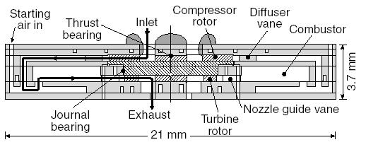
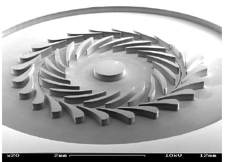
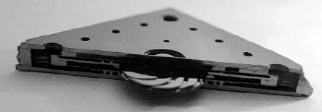
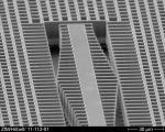
8 Example: MEMS Microturbines
9 3. Overview of Microfabrication TOC Wafer-Level Processes Substrates Wafer Cleaning Oxidation Doping Thin-Film Deposition Wafer Bonding
10 3. Overview of Microfabrication TOC Pattern Transfer Optical Lithography Design Rules Mask Making Wet Etching Dry-Etching Lift-Off Planarization
11 3. Overview of Microfabrication TOC Wafer-Level Processes Substrates Wafer Cleaning Oxidation Doping Thin-Film Deposition Wafer Bonding
12
13
14
15
16
17
18
19

20
21
22
23
24
25
26
27
28
29
30 Ga + Ga + Ga + Ga + Ga + Doping by Ion Implantation

31 Doping by Ion Implantation (ctnd.)
32 Doping by Ion Implantation (ctnd.)
33 Doping by Ion Implantation (ctnd.)
34
35

36 Doping by Ion Implantation (example)
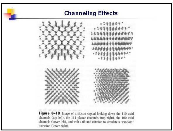
37 Channeling Effects
38
39 Channeling Effects (ctnd.)

40 Ion implantation for production of buried oxide

41 Cross-section of SIMOX wafers
42
43
44
45
46
47
48 3. Overview of Microfabrication TOC Wafer-Level Processes Substrates Wafer Cleaning Oxidation Doping Thin-Film Deposition Wafer Bonding
49 Electronic Materials Typical IC materials include: Thermal oxides (covered previously) Other Dielectric Materials Poly-crystalline silicon (Poly-Si) Metals
50 Electronic Materials Typical IC materials include: Thermal oxides (covered previously) Other Dielectric Materials Poly-crystalline silicon (Poly-Si) Metals
51 Chemical Vapor Deposition SiO 2 Field Oxide Interlevel Insulator Passivation (overcoat layer) Si 3 N 4 Local Oxidation Mask Protective Overcoat Layer Gate Dielectric Poly-Si Gate Material in MOSFET Metallization Inerconnects Epitaxial Layers Si Ge GaAs GaP Purpose: low temperature deposition of insulators and conductors
52 Chemical Vapor Deposition (CVD) C A B A : Gaseous transport and adsorption of precursor B: Surface transport and reaction C: Desorption of by-products
53 Chemical Vapor Deposition (ctnd ) For SiO 2 : 500 o C SiH 4 + O 2 SiO H 2 For Si 3 N 4 : 900 o C SiCl 2 H H 2 O SiO H HCl 800 o C 3SiCl 2 H NH 3 Si 3 N HCl + 6 H 2 For Poly-Si: SiH o C Si + 2 H 2
54 Low Pressure CVD (LPCVD)
55 Plasma-enhanced CVD (PECVD)
56 Properties of Oxide Films
57 Sputtering
58 Electronic Materials Typical IC materials include: Thermal oxides (covered previously) Other Dielectric Materials Poly-crystalline silicon (Poly-Si) Metals
59 Metallization

60 Metallization by evaporation
61 3. Overview of Microfabrication TOC Wafer-Level Processes Substrates Wafer Cleaning Oxidation Doping Thin-Film Deposition Wafer Bonding

62 Wafer bonding Used to permanently join two wafers together Allows the design and fabrication of multi-level devices assembled from the machining of separate wafers Fundamentals of process not fully understood, but does rely on formation of Si-O-Si bonds between wafers.
63 MEMS microturbines

64 Wafer bonding by fusion (ctnd.)
65 Fusion bonding procedures 1.Surface treatment to make hydrophilic surfaces by soaking wafers in Piranha, diluted sulfuric acid, or boiling nitric acid, or hydrophobic surfaces in HF. Hydrophilic top layer consisting of O-H bonds (hydroxyl) is formed on the oxide surface. 2.Contacting the wafers in clean air at room temperature after rinsing and drying them. Self-bonding (hydrogen bonding) is formed throughout the wafer surfaces without external pressure with considerable forces. 3.Annealing (> 800 o C) in oxidizing or nonoxidizing ambient. Water molecules come out and the voids (intrinsic) are observed beyond 200 o C. The voids tend to disappear and bonding strength is increased at more than 300 o C forming siloxane (Si-O) bonds. At high temperatures (>800 o C), Oxygen at the interface may diffuse into the silicon bulk to form Si-Si bonds like single crystal silicon at above 1000 o C.
66 Wafer bonding by fusion
67 Thermal considerations in fusion bonding 1. Temperature less than 450 C for postmetallisation wafers. 2. Temperature less than 800 C for wafers with diffusion dopant layers (e.g. p + etch-stop layers). 3. Temperature greater than 1000 C for wafer bonding before processing. According to the reaction mechanism, annealing at temperatures above 1000 C for several hours should result in an almost complete reaction of the interface. A 1000 C anneal for about two hours gives sufficiently high bond strength for all subsequent treatments (Harendt et al. 1991); it is not possible to separate the two bonded Si wafers without breaking the silicon.

68 Anodic bonding : principle
69 Anodic bonding : principle (ctnd.)
70 Anodic bonding : principle (ctnd.) General Principles: Due to the elevated temperature, the Na+ ions are mobile enough for the Pyrex to behave like a conductor. Hence, in the very first moment, most of the voltage applied to the silicon- Pyrex sandwich drops across a small gap of a few microns between the two surfaces. The high electric field in this area creates a strong electrostatic force, pulling the two surfaces together and thus forming an intimate contact. In addition Na+ ions start drifting to the negative electrode, which is connected with glass, creating depletion zone adjacent to the silicon, positive electrode. During this charging process, the electric field is high enough to allow a drift of oxygen to the positive electrode (Si) reacting with silicon and creating Si-O bond.
71 Anodic bonding setup Glass sputtered onto one of the silicon surfaces Bonding take place at T ~ C, at V = V (greatly varies depending on glass used for bonding)
72 Anodic bonding : procedure Typical Variables: temperature, applied voltage, bonding load, voltage-applying time, bonding area, glass thickness o C, V. (FYI: Temperature limit for IC processed Si substrates is about 450 o C) General conditions: Silicon + Pyrex 7740, 400 o C, and 1000V. Requirements: Microroughness (Ra) < 1μm. Warp/bow < 5μm The native or thermal oxide layer on the Si must be thinner than 2000Å. Benefits: Lower temperature process and popular and reliable process Less stringent requirement for the surface quality of the wafers.


73 Alternate bonding technique : eutectic bonding One wafer coated with Au prior to bonding Temperature is raised until the Eutectic point is reached Above eutectic temperature, Au will diffuse into Si (and not other way around An Au-Si eutectic alloy is then formed between the two wafers Other Si-metal alloys eutecic bonding also possible

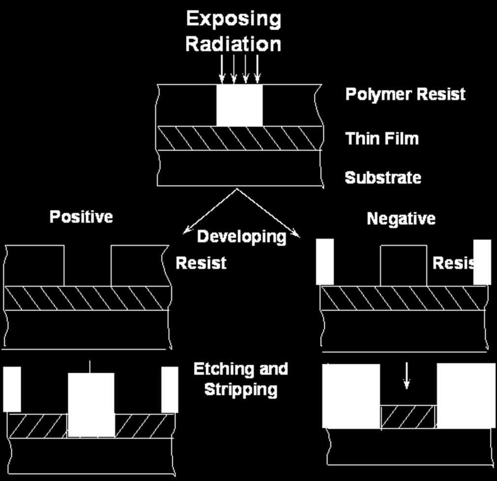
74 IR monitoring of bonded wafers Quality of bonds is usually monitored using infrared absorption imaging
75 Worked Example : floating element shear sensor (a) Angled view and (b) cross section of a floating sensor based on a rectangular plate with four tethers
76 Worked Example : floating element shear sensor Si SiO2 Si A better view of geometry of such device
77 Worked example : floating element shear sensor
78 Worked example : floating element shear sensor
79 3. Overview of Microfabrication TOC Pattern Transfer Optical Lithography Design Rules Mask Making Wet Etching Dry-Etching Lift-Off Planarization
80 3. Overview of Microfabrication TOC Pattern Transfer Optical Lithography Design Rules Mask Making Wet Etching Dry-Etching Lift-Off Planarization
81 Elements of photolithography
82 Elements of photolithography (ctnd.) Lithography consists of patterning substrate by employing the interaction of beams of photons or particles with materials. Photolithography is widely used in the integrated circuits (ICs) manufacturing. The process of IC manufacturing consists of a series of steps or more, called mask layers where layers of materials coated with resists are patterned then transferred onto the material layer.
83 Elements of photolithography (ctnd.) A photolithography system consists of a light source, a mask, and a optical projection system. Photoresists are radiation sensitive materials that usually consist of a photo-sensitive compound, a polymeric backbone, and a solvent. Resists can be classified upon their solubility after exposure into: positive resists (solubility of exposed area increases) and negative resists (solubility of exposed area decreases).

84 Positive vs. negative photoresists

85 Types of photolithography Contact Printing Proximity Printing Projection Printing
86 Types of photolithography (ctnd.) Contact lithography limited by Fresnel diffraction: W min = λg where λ is wavelength employed and g is mask-resist gap.
87 Types of photolithography (ctnd.) Projection lithography limited by Rayleigh's criterion: k R = 1λ NA where λ is wavelength employed, NA is numerical aperture of lense (NA = sin α), and k 1 is a constant (typically k 1 = )
88 Resolution of photolithography: example Question: An x-ray contact lithography system uses photons of energy of 1 kev. If the separation between the mask and the wafer is 20 μm, estimate the diffractionlimited resolution that is achievable by this system Answer: The energy E p of photons is related to their wavelength λ through: = hc λ where h = m 2 kg/s is Planck s constant, and c = 3 x 10 8 m/s is the speed of light. Thus, the wavelength of the photons employed is: E p λ λ x10 3x10 = x10 = 1.24 nm 8 The minimum feature size that can be resolved is: W min = λg W 9 6 min = 1.24x10 20x10 W min = 157 nm

89 Resolution of photolithography (ctnd.)


90 Resol. enhancement : phase shift masks (ctnd) 120 nm wide gates produced using λ = 248 nm radiation and PSM masks

91 Resolution enhancement : immersion lithography - In immersion lithography, the medium through which the exposure light passes is purified water, with a refractive index of 1.44, rather than air. - Therefore, the NA can be increased by a factor of up to 1.44, which will enable to surpass the barrier of the 65nm line width, which is considered the limit for ArF steppers. - Theoretically, the technology is expected to be capable of extending micro processing down to the 45nm line width.
 One in every home.")
92 EUV lithography system (ctnd.) One in every home...
93 Alternate Nanolithography Techniques Micro-contact Printing Nanoimprint Lithography Scanned Probe Lithography Dip-pen Lithography
 Removal of stamp 4) Residues rinsed off Source: IBM")
94 Micro-contact printing 1) Application of ink to stamp 2) Application of stamp to surface 3) Removal of stamp 4) Residues rinsed off Source: IBM Zurich


95 Selective growth of neurons on printed surfaces Biological interactions that underlie neuron cell attachment and growth are being employed to produce defined networks of neurons. Microcontact printing has been used to place chemical, biochemical, and/or topographical cues at designated locations. Important potential for the interfacing of solid state electronics with nerve cell biology, and for the fundamental electrical studies of single nerve cells. Source: Craighead Group, Cornell Selective growth of neurons on chemically patterned Si (C. D. James et al.)
96 Alternate Nanolithography Techniques Micro-contact Printing Nanoimprint Lithography Scanned Probe Lithography Dip-pen Lithography

97 Nanoimprint Lithography Consists of pressing a mold onto the resist above its glass transition temperature T g More? Check out S. Y. Chou, Princeton

98 NIL master SiO 2 pillars with 10 nm diameter, 40 nm spacing, and 60 nm height fabricated by e-beam lithography. This master can be used tens of times for the imprinting of holes in PMMA without degradation
, P= 4.4 MPa. PMMA conforms to master patterng, resulting in ~10 nm range holes")
99 NIL pattern in PMMA Mask is pressed into 80 nm thick layer of PMMA on Si substrate at 175 C (T g =105 C), P= 4.4 MPa. PMMA conforms to master patterng, resulting in ~10 nm range holes

100 Metal dots by NIL Reactive ion etching is used to cut down resist thickness until shallow regions are completely removed Ti/Au is deposited onto resist. Resist and metalcoating is removed by solvent leaving behind metal dots where resist had been removed.
101 Alternate Nanolithography Techniques Micro-contact Printing Nanoimprint Lithography Scanned Probe Lithography Dip-pen Lithography

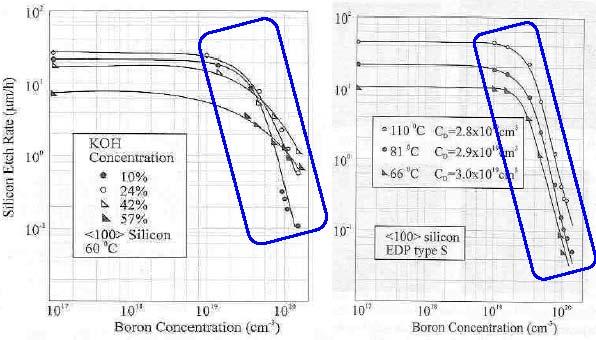
102 Scanned Probe Lithography Source: Quate Group, Stanford


103 Fabrication of CMOS gate using SPM lithography Source: Quate Group, Stanford
104 Alternate Nanolithography Techniques Micro-contact Printing Nanoimprint Lithography Scanned Probe Lithography Dip-pen Lithography

105 Source: Mirkin Group, NWU Dip-pen lithography
 DPN generated multi-component nanostructure with two aligned alkanethiol patterns.")
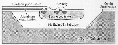
106 Dip-pen lithography A) Ultra-high resolution pattern of mercaptohexadecanoic acid on atomically-flat gold surface. B) DPN generated multi-component nanostructure with two aligned alkanethiol patterns. C) Richard Feynmann's historic speech written using the DPN nanoplotter Source: Mirkin Group, NWU
107 3. Overview of Microfabrication TOC Pattern Transfer Optical Lithography Design Rules Mask Making (read) Wet Etching Dry-Etching Lift-Off Planarization
108 3. Overview of Microfabrication TOC Pattern Transfer Optical Lithography Design Rules Mask Making (read) Wet Etching Dry-Etching Lift-Off Planarization
109 Need for Wet Etching.

110 Wet Etching.


111 Isotropic vs anisotropic etching : etching bias
112 Degree of anisotropy
113 Anisotropic etchants in silicon w = w 0-2h cot (55 o )
114 Anisotropic etchants in silicon (ctnd.)

115 KOH etch of Si

116 Example MEMS Velcro
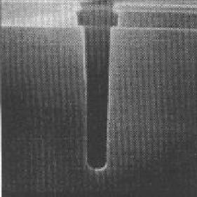
117 Example : MEMS Velcro (ctnd.)

118 Need for etch-stopping layers
119 Need for etch-stopping layers (ctnd.)
120 Doping-selective etching
121 Doping-selective etching (ctnd.) Disadvantage: requires high-dopant concentration to achieve good selectivity

122 Electrochemical etching Steps 1. Injection of holes into the semiconductor to raise it to a higher oxidation state Si + 2. Attachment of negatively charged hydroxyl groups, OH -, to the positively charged Si 3. Reaction of the hydrated silicon with the complexing agent in the solution 4. Dissolution of the reaction products into the etchant solution
123 Electrochemical etching ctnd.) Plot of electrochemical current density against voltage for silicon doped to different resistivities
 Current-voltage characteristics of n-si and p-si in KOH.")
124 Electrochemical etch stop (ctnd.) Current-voltage characteristics of n-si and p-si in KOH. No current flows at the OCP and the current stops above the passivating potential
125 Example #1: fabrication of membranes Method to fabricate an array of thin membranes: (a) design of an oxide mask and (b) the electrochemical cell providing a back etch
126 Example #2 : fabrication of cantilevers
127 Example #2 : fabrication of cantilevers (ctnd.)
128 3. Overview of Microfabrication TOC Pattern Transfer Optical Lithography Design Rules Mask Making (read) Wet Etching Dry-Etching Lift-Off Planarization
129 Plasma Etching
130 Plasma Induced Etching Process

131 Plasma Induced Etching Process (ctnd.)


132 Etched Structures Advantages -Good directional etching -Good Selectivity of SiO2 to Si
133 SCREAM process overview
134 SCREAM process overview (ctnd.)

135 Example of structures produced by SCREAM
136 3. Overview of Microfabrication TOC Pattern Transfer Optical Lithography Design Rules Mask Making (read) Wet Etching Dry-Etching Lift-Off Planarization
137
138 3. Overview of Microfabrication TOC Pattern Transfer Optical Lithography Design Rules Mask Making (read) Wet Etching Dry-Etching Lift-Off Planarization (read)
EECS130 Integrated Circuit Devices
 EECS130 Integrated Circuit Devices Professor Ali Javey 9/13/2007 Fabrication Technology Lecture 1 Silicon Device Fabrication Technology Over 10 15 transistors (or 100,000 for every person in the world)
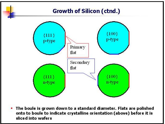
Czochralski Crystal Growth
 Czochralski Crystal Growth Crystal Pulling Crystal Ingots Shaping and Polishing 300 mm wafer 1 2 Advantage of larger diameter wafers Wafer area larger Chip area larger 3 4 Large-Diameter Wafer Handling
Chapter 3 Silicon Device Fabrication Technology
 Chapter 3 Silicon Device Fabrication Technology Over 10 15 transistors (or 100,000 for every person in the world) are manufactured every year. VLSI (Very Large Scale Integration) ULSI (Ultra Large Scale
EE40 Lec 22. IC Fabrication Technology. Prof. Nathan Cheung 11/19/2009
 Suggested Reading EE40 Lec 22 IC Fabrication Technology Prof. Nathan Cheung 11/19/2009 300mm Fab Tour http://www-03.ibm.com/technology/manufacturing/technology_tour_300mm_foundry.html Overview of IC Technology
Introduction to Lithography
 Introduction to Lithography G. D. Hutcheson, et al., Scientific American, 290, 76 (2004). Moore s Law Intel Co-Founder Gordon E. Moore Cramming More Components Onto Integrated Circuits Author: Gordon E.
Introduction to Micro/Nano Fabrication Techniques. Date: 2015/05/22 Dr. Yi-Chung Tung. Fabrication of Nanomaterials
 Introduction to Micro/Nano Fabrication Techniques Date: 2015/05/22 Dr. Yi-Chung Tung Fabrication of Nanomaterials Top-Down Approach Begin with bulk materials that are reduced into nanoscale materials Ex:
Lecture #18 Fabrication OUTLINE
 Transistors on a Chip Lecture #18 Fabrication OUTLINE IC Fabrication Technology Introduction the task at hand Doping Oxidation Thin-film deposition Lithography Etch Lithography trends Plasma processing
Surface Micromachining
 Surface Micromachining Micro Actuators, Sensors, Systems Group University of Illinois at Urbana-Champaign Outline Definition of surface micromachining Most common surface micromachining materials - polysilicon
Microstructure of Electronic Materials. Amorphous materials. Single-Crystal Material. Professor N Cheung, U.C. Berkeley
 Microstructure of Electronic Materials Amorphous materials Single-Crystal Material 1 The Si Atom The Si Crystal diamond structure High-performance semiconductor devices require defect-free crystals 2 Crystallographic
EE 5344 Introduction to MEMS. CHAPTER 3 Conventional Si Processing
 3. Conventional licon Processing Micromachining, Microfabrication. EE 5344 Introduction to MEMS CHAPTER 3 Conventional Processing Why silicon? Abundant, cheap, easy to process. licon planar Integrated
Lecture 22: Integrated circuit fabrication
 Lecture 22: Integrated circuit fabrication Contents 1 Introduction 1 2 Layering 4 3 Patterning 7 4 Doping 8 4.1 Thermal diffusion......................... 10 4.2 Ion implantation.........................
PHYS 534 (Fall 2008) Process Integration OUTLINE. Examples of PROCESS FLOW SEQUENCES. >Surface-Micromachined Beam
 Process Integration OUTLINE. Examples of PROCESS FLOW SEQUENCES. >Surface-Micromachined Beam") PHYS 534 (Fall 2008) Process Integration Srikar Vengallatore, McGill University 1 OUTLINE Examples of PROCESS FLOW SEQUENCES >Semiconductor diode >Surface-Micromachined Beam Critical Issues in Process
PHYS 534 (Fall 2008) Process Integration Srikar Vengallatore, McGill University 1 OUTLINE Examples of PROCESS FLOW SEQUENCES >Semiconductor diode >Surface-Micromachined Beam Critical Issues in Process
Chemical Vapor Deposition
 Chemical Vapor Deposition ESS4810 Lecture Fall 2010 Introduction Chemical vapor deposition (CVD) forms thin films on the surface of a substrate by thermal decomposition and/or reaction of gas compounds
Microelectronics. Integrated circuits. Introduction to the IC technology M.Rencz 11 September, Expected decrease in line width
 Microelectronics Introduction to the IC technology M.Rencz 11 September, 2002 9/16/02 1/37 Integrated circuits Development is controlled by the roadmaps. Self-fulfilling predictions for the tendencies
ELEC 3908, Physical Electronics, Lecture 4. Basic Integrated Circuit Processing
 ELEC 3908, Physical Electronics, Lecture 4 Basic Integrated Circuit Processing Lecture Outline Details of the physical structure of devices will be very important in developing models for electrical behavior
Surface micromachining and Process flow part 1
 Surface micromachining and Process flow part 1 Identify the basic steps of a generic surface micromachining process Identify the critical requirements needed to create a MEMS using surface micromachining
Mostafa Soliman, Ph.D. May 5 th 2014
 Mostafa Soliman, Ph.D. May 5 th 2014 Mostafa Soliman, Ph.D. 1 Basic MEMS Processes Front-End Processes Back-End Processes 2 Mostafa Soliman, Ph.D. Wafers Deposition Lithography Etch Chips 1- Si Substrate
Chapter 2 MOS Fabrication Technology
 Chapter 2 MOS Fabrication Technology Abstract This chapter is concerned with the fabrication of metal oxide semiconductor (MOS) technology. Various processes such as wafer fabrication, oxidation, mask
Chapter 3 CMOS processing technology
 Chapter 3 CMOS processing technology (How to make a CMOS?) Si + impurity acceptors(p-type) donors (n-type) p-type + n-type => pn junction (I-V) 3.1.1 (Wafer) Wafer = A disk of silicon (0.25 mm - 1 mm thick),
Fabrication Technology, Part I
 EEL5225: Principles of MEMS Transducers (Fall 2003) Fabrication Technology, Part I Agenda: Oxidation, layer deposition (last lecture) Lithography Pattern Transfer (etching) Impurity Doping Reading: Senturia,
Fabrication and Layout
 ECEN454 Digital Integrated Circuit Design Fabrication and Layout ECEN 454 3.1 A Glimpse at MOS Device Polysilicon Aluminum ECEN 475 4.2 1 Material Classification Insulators Glass, diamond, silicon oxide
Lect. 2: Basics of Si Technology
 Unit processes Thin Film Deposition Etching Ion Implantation Photolithography Chemical Mechanical Polishing 1. Thin Film Deposition Layer of materials ranging from fractions of nanometer to several micro-meters
Fabrication Technology, Part II
 EEL5225: Principles of MEMS Transducers (Fall 2003) Fabrication Technology, Part II Agenda: Process Examples TI Micromirror fabrication process SCREAM CMOS-MEMS processes Wafer Bonding LIGA Reading: Senturia,
Semiconductor Technology
 Semiconductor Technology from A to Z Oxidation www.halbleiter.org Contents Contents List of Figures List of Tables II III 1 Oxidation 1 1.1 Overview..................................... 1 1.1.1 Application...............................
ECE 440 Lecture 27 : Equilibrium P-N Junctions I Class Outline:
 ECE 440 Lecture 27 : Equilibrium P-N Junctions I Class Outline: Fabrication of p-n junctions Contact Potential Things you should know when you leave Key Questions What are the necessary steps to fabricate
Today s Class. Materials for MEMS
 Lecture 2: VLSI-based Fabrication for MEMS: Fundamentals Prasanna S. Gandhi Assistant Professor, Department of Mechanical Engineering, Indian Institute of Technology, Bombay, Recap: Last Class What is
Microfabrication of Integrated Circuits
 Microfabrication of Integrated Circuits OUTLINE History Basic Processes Implant; Oxidation; Photolithography; Masks Layout and Process Flow Device Cross Section Evolution Lecture 38, 12/05/05 Reading This
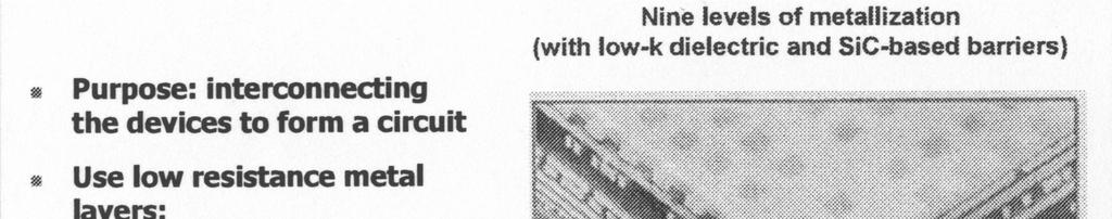
Complexity of IC Metallization. Early 21 st Century IC Technology
 EECS 42 Introduction to Digital Electronics Lecture # 25 Microfabrication Handout of This Lecture. Today: how are Integrated Circuits made? Silicon wafers Oxide formation by growth or deposition Other
3.155J / 6.152J Micro/Nano Processing Technology TAKE-HOME QUIZ FALL TERM 2005
 3.155J / 6.152J Micro/Nano Processing Technology TAKE-HOME QUIZ FALL TERM 2005 1) This is an open book, take-home quiz. You are not to consult with other class members or anyone else. You may discuss the
Most semiconductor devices contain at least one junction between p-type and n-type material. These p-n junctions are fundamental to the performance
 Ch. 5: p-n Junction Most semiconductor devices contain at least one junction between p-type and n-type material. These p-n junctions are fundamental to the performance of functions such as rectification,
General Introduction to Microstructure Technology p. 1 What is Microstructure Technology? p. 1 From Microstructure Technology to Microsystems
 General Introduction to Microstructure Technology p. 1 What is Microstructure Technology? p. 1 From Microstructure Technology to Microsystems Technology p. 9 The Parallels to Microelectronics p. 15 The
IC/MEMS Fabrication - Outline. Fabrication
 IC/MEMS Fabrication - Outline Fabrication overview Materials Wafer fabrication The Cycle: Deposition Lithography Etching Fabrication IC Fabrication Deposition Spin Casting PVD physical vapor deposition
Fabrication Process. Crystal Growth Doping Deposition Patterning Lithography Oxidation Ion Implementation CONCORDIA VLSI DESIGN LAB
 Fabrication Process Crystal Growth Doping Deposition Patterning Lithography Oxidation Ion Implementation 1 Fabrication- CMOS Process Starting Material Preparation 1. Produce Metallurgical Grade Silicon
CS/ECE 5710/6710. N-type Transistor. N-type from the top. Diffusion Mask. Polysilicon Mask. CMOS Processing
 CS/ECE 5710/6710 CMOS Processing Addison-Wesley N-type Transistor D G +Vgs + Vds S N-type from the top i electrons - Diffusion Mask Mask for just the diffused regions Top view shows patterns that make
Manufacturing Technologies for MEMS and SMART SENSORS
 4 Manufacturing Technologies for MEMS and SMART SENSORS Dr. H. K. Verma Distinguished Professor (EEE) Sharda University, Greater Noida (Formerly: Deputy Director and Professor of Instrumentation Indian
The Physical Structure (NMOS)
") The Physical Structure (NMOS) Al SiO2 Field Oxide Gate oxide S n+ Polysilicon Gate Al SiO2 SiO2 D n+ L channel P Substrate Field Oxide contact Metal (S) n+ (G) L W n+ (D) Poly 1 3D Perspective 2 3 Fabrication
The Physical Structure (NMOS) Al SiO2 Field Oxide Gate oxide S n+ Polysilicon Gate Al SiO2 SiO2 D n+ L channel P Substrate Field Oxide contact Metal (S) n+ (G) L W n+ (D) Poly 1 3D Perspective 2 3 Fabrication
Lecture 19 Microfabrication 4/1/03 Prof. Andy Neureuther
 EECS 40 Spring 2003 Lecture 19 Microfabrication 4/1/03 Prof. ndy Neureuther How are Integrated Circuits made? Silicon wafers Oxide formation by growth or deposition Other films Pattern transfer by lithography
Review of CMOS Processing Technology
 - Scaling and Integration Moore s Law Unit processes Thin Film Deposition Etching Ion Implantation Photolithography Chemical Mechanical Polishing 1. Thin Film Deposition Layer of materials ranging from
EE 330 Lecture 8. IC Fabrication Technology Part II. - Oxidation - Epitaxy - Polysilicon - Interconnects
 EE 330 Lecture 8 IC Fabrication Technology Part II - Oxidation - Epitaxy - Polysilicon - Interconnects Review from Last Time MOS Transistor Bulk Source Gate Drain p-channel MOSFET Lightly-doped n-type
A discussion of crystal growth, lithography, etching, doping, and device structures is presented in
 Chapter 5 PROCESSING OF DEVICES A discussion of crystal growth, lithography, etching, doping, and device structures is presented in the following overview gures. SEMICONDUCTOR DEVICE PROCESSING: AN OVERVIEW
VLSI Technology. By: Ajay Kumar Gautam
 By: Ajay Kumar Gautam Introduction to VLSI Technology, Crystal Growth, Oxidation, Epitaxial Process, Diffusion Process, Ion Implantation, Lithography, Etching, Metallization, VLSI Process Integration,
L5: Micromachining processes 1/7 01/22/02
 97.577 L5: Micromachining processes 1/7 01/22/02 5: Micromachining technology Top-down approaches to building large (relative to an atom or even a transistor) structures. 5.1 Bulk Micromachining A bulk
PROCESS FLOW AN INSIGHT INTO CMOS FABRICATION PROCESS
 Contents: VI Sem ECE 06EC63: Analog and Mixed Mode VLSI Design PROCESS FLOW AN INSIGHT INTO CMOS FABRICATION PROCESS 1. Introduction 2. CMOS Fabrication 3. Simplified View of Fabrication Process 3.1 Alternative
Silicon Manufacturing
 Silicon Manufacturing Group Members Young Soon Song Nghia Nguyen Kei Wong Eyad Fanous Hanna Kim Steven Hsu th Fundamental Processing Steps 1.Silicon Manufacturing a) Czochralski method. b) Wafer Manufacturing
Dr. Priyabrat Dash Office: BM-406, Mob: Webpage: MB: 205
 Email: dashp@nitrkl.ac.in Office: BM-406, Mob: 8895121141 Webpage: http://homepage.usask.ca/~prd822/ MB: 205 Nonmanufacturing In continuation from last class... 2 Top-Down methods Mechanical-energy methods
EE 330 Lecture 9. IC Fabrication Technology Part II. -Oxidation -Epitaxy -Polysilicon -Planarization -Resistance and Capacitance in Interconnects
 EE 330 Lecture 9 IC Fabrication Technology Part II -Oxidation -Epitaxy -Polysilicon -Planarization -Resistance and Capacitance in Interconnects Review from Last Time IC Fabrication Technology Crystal Preparation
EE 330 Lecture 9. IC Fabrication Technology Part 2
 EE 330 Lecture 9 IC Fabrication Technology Part 2 Quiz 8 A 2m silicon crystal is cut into wafers using a wire saw. If the wire diameter is 220um and the wafer thickness is 350um, how many wafers will this
Micromachining AMT 2505
 Micromachining AMT 2505 Shanmuga Raja.B (BVB0912004) Module leader : Mr. Raja Hussain Introduction Micromachining are inherently connected to the evolution of Micro Electro Mechanical Systems (MEMS). Decades
Lecture 5. SOI Micromachining. SOI MUMPs. SOI Micromachining. Silicon-on-Insulator Microstructures. Agenda:
 EEL6935 Advanced MEMS (Spring 2005) Instructor: Dr. Huikai Xie SOI Micromachining Agenda: SOI Micromachining SOI MUMPs Multi-level structures Lecture 5 Silicon-on-Insulator Microstructures Single-crystal
EE 330 Lecture 8. IC Fabrication Technology Part II. - Masking - Photolithography - Deposition - Etching - Diffusion
 EE 330 Lecture 8 IC Fabrication Technology Part II?? - Masking - Photolithography - Deposition - Etching - Diffusion Review from Last Time Technology Files Provide Information About Process Process Flow
CMOS Technology. Flow varies with process types & company. Start with substrate selection. N-Well CMOS Twin-Well CMOS STI
 CMOS Technology Flow varies with process types & company N-Well CMOS Twin-Well CMOS STI Start with substrate selection Type: n or p Doping level, resistivity Orientation, 100, or 101, etc Other parameters
ME 189 Microsystems Design and Manufacture. Chapter 9. Micromanufacturing
 ME 189 Microsystems Design and Manufacture Chapter 9 Micromanufacturing This chapter will offer an overview of the application of the various fabrication techniques described in Chapter 8 in the manufacturing
Mikrosensorer. Microfabrication 1
 Mikrosensorer Microfabrication 1 Literature Introductory MEMS Fabrication and Applications Thomas M. Adams and Richard A. Layton Available as ebook on http://www.lub.lu.se/en/search/lubsearch.html This
Metallization deposition and etching. Material mainly taken from Campbell, UCCS
 Metallization deposition and etching Material mainly taken from Campbell, UCCS Application Metallization is back-end processing Metals used are aluminum and copper Mainly involves deposition and etching,
Ajay Kumar Gautam [VLSI TECHNOLOGY] VLSI Technology for 3RD Year ECE/EEE Uttarakhand Technical University
![Ajay Kumar Gautam [VLSI TECHNOLOGY] VLSI Technology for 3RD Year ECE/EEE Uttarakhand Technical University](/thumbs/75/72824557.jpg "Ajay Kumar Gautam [VLSI TECHNOLOGY] VLSI Technology for 3RD Year ECE/EEE Uttarakhand Technical University") 2014 Ajay Kumar Gautam [VLSI TECHNOLOGY] VLSI Technology for 3RD Year ECE/EEE Uttarakhand Technical University Page1 Syllabus UNIT 1 Introduction to VLSI Technology: Classification of ICs, Scale of integration,
2014 Ajay Kumar Gautam [VLSI TECHNOLOGY] VLSI Technology for 3RD Year ECE/EEE Uttarakhand Technical University Page1 Syllabus UNIT 1 Introduction to VLSI Technology: Classification of ICs, Scale of integration,
Doping and Oxidation
 Technische Universität Graz Institute of Solid State Physics Doping and Oxidation Franssila: Chapters 13,14, 15 Peter Hadley Technische Universität Graz Institute of Solid State Physics Doping Add donors
FABRICATION ENGINEERING MICRO- NANOSCALE ATTHE AND. Fourth Edition STEPHEN A. CAMPBELL. of Minnesota. University OXFORD UNIVERSITY PRESS
 AND FABRICATION ENGINEERING ATTHE MICRO- NANOSCALE Fourth Edition STEPHEN A. CAMPBELL University of Minnesota New York Oxford OXFORD UNIVERSITY PRESS CONTENTS Preface xiii prrt i OVERVIEW AND MATERIALS
More on VLSI Fabrication Technologies. Emanuele Baravelli
 More on VLSI Fabrication Technologies Emanuele Baravelli Some more details on: 1. VLSI meaning 2. p-si epitaxial layer 3. Lithography 4. Metallization 5. Process timings What does VLSI mean, by the way?
Fabrication Technology
 Fabrication Technology By B.G.Balagangadhar Department of Electronics and Communication Ghousia College of Engineering, Ramanagaram 1 OUTLINE Introduction Why Silicon The purity of Silicon Czochralski
Silicon Epitaxial CVD Want to create very sharp PN boundary grow one type layer on other in single crystal form High dopant layers on low dopant
 Silicon Epitaxial CVD Want to create very sharp PN boundary grow one type layer on other in single crystal form High dopant layers on low dopant substrate Creates latch up protection for CMOS Buried Epi
SURFACE MICROMACHINING
 SURFACE MICROMACHINING Features are built up, layer by layer on the surface of a substrate. Surface micromachined devices are much smaller than bulk micromachined components. Nature of deposition process
Micro-Electro-Mechanical Systems (MEMS) Fabrication. Special Process Modules for MEMS. Principle of Sensing and Actuation
 Fabrication. Special Process Modules for MEMS. Principle of Sensing and Actuation") Micro-Electro-Mechanical Systems (MEMS) Fabrication Fabrication Considerations Stress-Strain, Thin-film Stress, Stiction Special Process Modules for MEMS Bonding, Cavity Sealing, Deep RIE, Spatial forming
Micro-Electro-Mechanical Systems (MEMS) Fabrication Fabrication Considerations Stress-Strain, Thin-film Stress, Stiction Special Process Modules for MEMS Bonding, Cavity Sealing, Deep RIE, Spatial forming
Chapter 4 Fabrication Process of Silicon Carrier and. Gold-Gold Thermocompression Bonding
 Chapter 4 Fabrication Process of Silicon Carrier and Gold-Gold Thermocompression Bonding 4.1 Introduction As mentioned in chapter 2, the MEMs carrier is designed to integrate the micro-machined inductor
Polymer-based Microfabrication
 Polymer-based Microfabrication PDMS SU-8 PMMA Hydrogel 1 Soft Lithography Developed by Whitesides, et. al A set of techniques for microfabrication based on the use of lithography, soft substrate materials
Semiconductor Manufacturing Technology. IC Fabrication Process Overview
 Semiconductor Manufacturing Technology Michael Quirk & Julian Serda October 00 by Prentice Hall Chapter 9 IC Fabrication Process Overview /4 Objectives After studying the material in this chapter, you
FABRICATION OF CMOS INTEGRATED CIRCUITS. Dr. Mohammed M. Farag
 FABRICATION OF CMOS INTEGRATED CIRCUITS Dr. Mohammed M. Farag Outline Overview of CMOS Fabrication Processes The CMOS Fabrication Process Flow Design Rules EE 432 VLSI Modeling and Design 2 CMOS Fabrication
Lecture 1A: Manufacturing& Layout
 Introduction to CMOS VLSI Design Lecture 1A: Manufacturing& Layout David Harris Harvey Mudd College Spring 2004 Steven Levitan Fall 2008 1 The Manufacturing Process For a great tour through the IC manufacturing
Chapter 2 Manufacturing Process
 Digital Integrated Circuits A Design Perspective Chapter 2 Manufacturing Process 1 CMOS Process 2 CMOS Process (n-well) Both NMOS and PMOS must be built in the same silicon material. PMOS in n-well NMOS
Introduction to CMOS VLSI Design. Layout, Fabrication, and Elementary Logic Design
 Introduction to CMOS VLSI Design Layout, Fabrication, and Elementary Logic Design CMOS Fabrication CMOS transistors are fabricated on silicon wafer Lithography process similar to printing press On each
VLSI INTRODUCTION P.VIDYA SAGAR ( ASSOCIATE PROFESSOR) Department of Electronics and Communication Engineering, VBIT
 Department of Electronics and Communication Engineering, VBIT") VLSI INTRODUCTION P.VIDYA SAGAR ( ASSOCIATE PROFESSOR) contents UNIT I INTRODUCTION: Introduction to IC Technology MOS, PMOS, NMOS, CMOS & BiCMOS technologies. BASIC ELECTRICAL PROPERTIES : Basic Electrical
VLSI INTRODUCTION P.VIDYA SAGAR ( ASSOCIATE PROFESSOR) contents UNIT I INTRODUCTION: Introduction to IC Technology MOS, PMOS, NMOS, CMOS & BiCMOS technologies. BASIC ELECTRICAL PROPERTIES : Basic Electrical
EE 330 Lecture 9. IC Fabrication Technology Part II. -Oxidation -Epitaxy -Polysilicon -Planarization -Resistance and Capacitance in Interconnects
 EE 330 Lecture 9 IC Fabrication Technology Part II -Oxidation -Epitaxy -Polysilicon -Planarization -Resistance and Capacitance in Interconnects Review from Last Time Etching Dry etch (anisotropic) SiO
MEMS Fabrication. Beyond Integrated Circuits. MEMS Basic Concepts
 MEMS Fabrication Beyond Integrated Circuits MEMS Basic Concepts Uses integrated circuit fabrication techniques to make mechanical as well as electrical components on a single chip. Small size 1µm 1mm Typically
UT Austin, ECE Department VLSI Design 2. CMOS Fabrication, Layout Rules
 2. CMOS Fabrication, Layout, Design Rules Last module: Introduction to the course How a transistor works CMOS transistors This module: CMOS Fabrication Design Rules CMOS Fabrication CMOS transistors are
Silicon Epitaxial CVD Want to create very sharp PN boundary grow one type layer on other in single crystal form High dopant layers on low dopant
 Silicon Epitaxial CVD Want to create very sharp PN boundary grow one type layer on other in single crystal form High dopant layers on low dopant substrate Creates latch up protection for CMOS Buried Epi
3. Photolithography, patterning and doping techniques. KNU Seminar Course 2015 Robert Mroczyński
 3. Photolithography, patterning and doping techniques KNU Seminar Course 2015 Robert Mroczyński Critical technology processes Photolithography The aim of this process is to transfer (in the most accurate
6.777J/2.732J Design and Fabrication of Microelectromechanical Devices Spring Term Solution to Problem Set 2 (16 pts)
") 6.777J/2.732J Design and Fabrication of Microelectromechanical Devices Spring Term 2007 By Brian Taff (Adapted from work by Feras Eid) Solution to Problem Set 2 (16 pts) Issued: Lecture 4 Due: Lecture
6.777J/2.732J Design and Fabrication of Microelectromechanical Devices Spring Term 2007 By Brian Taff (Adapted from work by Feras Eid) Solution to Problem Set 2 (16 pts) Issued: Lecture 4 Due: Lecture
CHAPTER - 4 CMOS PROCESSING TECHNOLOGY
 CHAPTER - 4 CMOS PROCESSING TECHNOLOGY Samir kamal Spring 2018 4.1 CHAPTER OBJECTIVES 1. Introduce the CMOS designer to the technology that is responsible for the semiconductor devices that might be designed
Simple Cubic Crystal
 Starting Material Simple Cubic Crystal Crystal Planes offset by d/4 Diamond lattice cell (C, Si, Ge, etc.) face atom in FCC corner atom in FCC (100) plane (110) plane (111) plane Crystal Planes/Direction
INTEGRATED-CIRCUIT TECHNOLOGY
 INTEGRATED-CIRCUIT TECHNOLOGY 0. Silicon crystal growth and wafer preparation 1. Processing Steps 1.1. Photolitography 1.2. Oxidation 1.3. Layer Deposition 1.4. Etching 1.5. Diffusion 1.6 Backend: assembly,
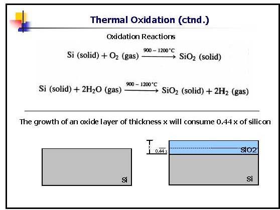
Chapter 4. UEEP2613 Microelectronic Fabrication. Oxidation
 Chapter 4 UEEP2613 Microelectronic Fabrication Oxidation Prepared by Dr. Lim Soo King 24 Jun 2012 Chapter 4...113 Oxidation...113 4.0 Introduction... 113 4.1 Chemistry of Silicon Dioxide Formation... 115
Nanoelectronics Fabrication Facility
 Nanoelectronics Fabrication Facility Contents Introduction 2 Mask Making Module 4 Photolithography Module 6 Wet Etching and CMP Module 8 Dry Etching and Sputtering Module 10 Thermal Process and Implantation
Chapter 2 OVERVIEW OF MEMS
 6 Chapter 2 OVERVIEW OF MEMS 2.1 MEMS and Microsystems The term MEMS is an abbreviation of microelectromechanical system. MEMS contains components ofsizes in 1 micrometer to 1 millimeter. The core element
Atomic Layer Deposition(ALD)
") Atomic Layer Deposition(ALD) AlO x for diffusion barriers OLED displays http://en.wikipedia.org/wiki/atomic_layer_deposition#/media/file:ald_schematics.jpg Lam s market-leading ALTUS systems combine CVD
Atomic Layer Deposition(ALD) AlO x for diffusion barriers OLED displays http://en.wikipedia.org/wiki/atomic_layer_deposition#/media/file:ald_schematics.jpg Lam s market-leading ALTUS systems combine CVD
Microelettronica. Planar Technology for Silicon Integrated Circuits Fabrication. 26/02/2017 A. Neviani - Microelettronica
 Microelettronica Planar Technology for Silicon Integrated Circuits Fabrication 26/02/2017 A. Neviani - Microelettronica Introduction Simplified crosssection of an nmosfet and a pmosfet Simplified crosssection
Lecture 5: Micromachining
 MEMS: Fabrication Lecture 5: Micromachining Prasanna S. Gandhi Assistant Professor, Department of Mechanical Engineering, Indian Institute of Technology, Bombay, Recap: Last Class E-beam lithography X-ray
Make sure the exam paper has 9 pages total (including cover page)
") UNIVERSITY OF CALIFORNIA College of Engineering Department of Electrical Engineering and Computer Sciences Fall 2010 EE143 Midterm Exam #2 Family Name First name SID Signature Solution Make sure the exam
UNIVERSITY OF CALIFORNIA College of Engineering Department of Electrical Engineering and Computer Sciences Fall 2010 EE143 Midterm Exam #2 Family Name First name SID Signature Solution Make sure the exam
Surface Micromachining
 Surface Micromachining Outline Introduction Material often used in surface micromachining Material selection criteria in surface micromachining Case study: Fabrication of electrostatic motor Major issues
Figure 2.3 (cont., p. 60) (e) Block diagram of Pentium 4 processor with 42 million transistors (2000). [Courtesy Intel Corporation.
 (e) Block diagram of Pentium 4 processor with 42 million transistors (2000). [Courtesy Intel Corporation.") Figure 2.1 (p. 58) Basic fabrication steps in the silicon planar process: (a) oxide formation, (b) selective oxide removal, (c) deposition of dopant atoms on wafer, (d) diffusion of dopant atoms into exposed
Figure 2.1 (p. 58) Basic fabrication steps in the silicon planar process: (a) oxide formation, (b) selective oxide removal, (c) deposition of dopant atoms on wafer, (d) diffusion of dopant atoms into exposed
2008 Summer School on Spin Transfer Torque
 2008 Summer School on Spin Transfer Torque Nano-scale device fabrication 2-July-2008 Byoung-Chul Min Center for Spintronics Research Korea Institute of Science and Technology Introduction Moore s Law
A Nano-thick SOI Fabrication Method
 A Nano-thick SOI Fabrication Method C.-H. Huang 1, J.T. Cheng 1, Y.-K. Hsu 1, C.-L. Chang 1, H.-W. Wang 1, S.-L. Lee 1,2, and T.-H. Lee 1,2 1 Dept. of Mechanical Engineering National Central University,
EE 143 FINAL EXAM NAME C. Nguyen May 10, Signature:
 INSTRUCTIONS Read all of the instructions and all of the questions before beginning the exam. There are 5 problems on this Final Exam, totaling 143 points. The tentative credit for each part is given to
VLSI Digital Systems Design
 VLSI Digital Systems Design CMOS Processing cmpe222_03process_ppt.ppt 1 Si Purification Chemical purification of Si Zone refined Induction furnace Si ingot melted in localized zone Molten zone moved from
Lecture 0: Introduction
 Lecture 0: Introduction Introduction Integrated circuits: many transistors on one chip. Very Large Scale Integration (VLSI): bucketloads! Complementary Metal Oxide Semiconductor Fast, cheap, low power
Dr. Lynn Fuller Webpage:
 ROCHESTER INSTITUTE OF TECHNOLOGY MICROELECTRONIC ENGINEERING Microelectromechanical Systems (MEMs) Process Integration Dr. Lynn Fuller Webpage: http://people.rit.edu/lffeee 82 Lomb Memorial Drive Rochester,
Physical Vapor Deposition (PVD) Zheng Yang
 Zheng Yang") Physical Vapor Deposition (PVD) Zheng Yang ERF 3017, email: yangzhen@uic.edu Page 1 Major Fabrication Steps in MOS Process Flow UV light Mask oxygen Silicon dioxide photoresist exposed photoresist oxide
Physical Vapor Deposition (PVD) Zheng Yang ERF 3017, email: yangzhen@uic.edu Page 1 Major Fabrication Steps in MOS Process Flow UV light Mask oxygen Silicon dioxide photoresist exposed photoresist oxide
Problem 1 Lab Questions ( 20 points total)
") Problem 1 Lab Questions ( 20 points total) (a) (3 points ) In our EE143 lab, we use Phosphorus for the source and drain diffusion. However, most advanced processes use Arsenic. What is the advantage of
Problem 1 Lab Questions ( 20 points total) (a) (3 points ) In our EE143 lab, we use Phosphorus for the source and drain diffusion. However, most advanced processes use Arsenic. What is the advantage of
Lecture Day 2 Deposition
 Deposition Lecture Day 2 Deposition PVD - Physical Vapor Deposition E-beam Evaporation Thermal Evaporation (wire feed vs boat) Sputtering CVD - Chemical Vapor Deposition PECVD LPCVD MVD ALD MBE Plating
PROCESSING OF INTEGRATED CIRCUITS
 PROCESSING OF INTEGRATED CIRCUITS Overview of IC Processing (Part I) Silicon Processing Lithography Layer Processes Use in IC Fabrication (Part II) Integrating the Fabrication Steps IC Packaging (Part
Welcome MNT Conference 1 Albuquerque, NM - May 2010
 Welcome MNT Conference 1 Albuquerque, NM - May 2010 Introduction to Design Outline What is MEMs Design General Considerations Application Packaging Process Flow What s available Sandia SUMMiT Overview