VLSI INTRODUCTION P.VIDYA SAGAR ( ASSOCIATE PROFESSOR) Department of Electronics and Communication Engineering, VBIT
|
|
|
- Melanie Randall
- 6 years ago
- Views:
Transcription


1 VLSI INTRODUCTION P.VIDYA SAGAR ( ASSOCIATE PROFESSOR)
2 contents UNIT I INTRODUCTION: Introduction to IC Technology MOS, PMOS, NMOS, CMOS & BiCMOS technologies. BASIC ELECTRICAL PROPERTIES : Basic Electrical Properties of MOS and BiCMOS Circuits: Ids-Vds relationships, MOS transistor threshold Voltage, gm, gds, figure of merit ωo ; Pass transistor, NMOS Inverter, Various pull ups, CMOS Inverter analysis and design, Bi-CMOS Inverters. 2
 25,000 parts cost: 17,470 3")
3 The First Computer The Babbage Difference Engine (1832) 25,000 parts cost: 17,470 3

4 ENIAC - The first electronic computer (1946) 4
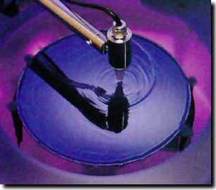
5 WHY VLSI? Integration Improves the Design Lower parasitics, higher clocking speed Lower power Physically small Integration Reduces Manufacturing Costs (almost) no manual assembly About $1-5billion/fab Typical Fab 1 city block, a few hundred people Packaging is largest cost Testing is second largest cost 5
6 Design Levels SYSTEM + MODULE GATE CIRCUIT S n+ G D n+ DEVICE 6
7 Moore s Law Gordon Moore cofounder of Intel Corporation visualized in the 1970 s that chip building technology would improve very quickly He projected that the number of transistors on a chip would double about every 18 months 7
8 INTEGRADED CIRCUIT (IC): Multi terminal electronic device in which discrete components like transistors,resisters,capacitors are fabricated in a single construction process. Classification of ICs : Based on application -Analog, digital Based on complexity -SSI, MSI, LSI, VLSI Based on fabrication-monolithic, hybrid Based on technology -RTL,DTL, TTL, MOS. 8
9 IC Evolution : SSI Small Scale Integration (early 1970s)-contained 1 10 logic gates MSI Medium Scale Integration-logic functions, counters LSI Large Scale Integration-first microprocessors on the chip VLSI Very Large Scale Integration-now offers 64-bit microprocessors, complete with cache memory (L1 and often L2),floating-point arithmetic unit(s), etc. Bipolar technology TTL (transistor-transistor logic) ECL (emitter-coupled logic) 9
10 Metal-oxide-semiconductor (MOS) and related VLSI technology MOS (Metal-oxide-silicon) although invented before bipolar transistor, was initially difficult to manufacture nmos (n-channel MOS) technology developed in 1970s required fewer masking steps, was denser, and consumed less power than equivalent bipolar Ics. CMOS (Complementary MOS): n-channel and p-channel MOS transistors => lower power consumption, simplified fabrication process Bi-CMOS - hybrid Bipolar, CMOS (for high speed) GaAs - Gallium Arsenide (for high speed) Si-Ge - Silicon Germanium (for RF) 10
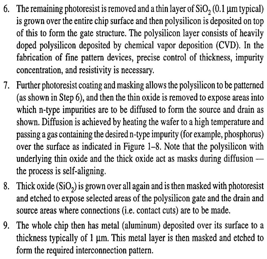
11 Mos transistors Basic MOS transistors with the doping concentration of transistor two types of MOS transistors are available as NMOS transistor and PMOS transistor. With their mode of operation further they are classified as depletion mode transistor and enhancement mode transistor. nmos enhancement mode transistor nmos devices are formed in a p-type substrate of moderate doping level. The source and drain regions are formed by diffusing n-type impurities through suitable masks into these areas. Thus source and drain are isolated from one another by two diodes and their Connections are made by a deposited metal layer. The basic block diagrams of nmos enhancement mode transistor is shown in figure. 11

12 nmos enhancement mode transistor nmos depletion mode transistor The basic block diagram of nmos depletion mode transistor is shown in figure. In depletion mode transistor the channel is established even the voltage Vgs = 0 by implanting suitable impurities in the region between source and drain during manufacture and prior to depositing the insulation and the gate. 12
13 MOS Transistors Four terminal device: gate, source, drain, body Polysilicon SiO 2 Source Gate Drain Gate oxide body stack looks like a capacitor p+ p+ n bulk Si Gate and body are conductors (body is also called the substrate) SiO2 (oxide) is a good insulator (separates the gate from the body Source Gate Drain Polysilicon SiO 2 Called metal oxide semiconductor (MOS) capacitor, even though gate is mostly made of poly-crystalline silicon (polysilicon) n+ p n+ bulk Si NMOS PMOS 13
14 Transistors as Switches We can view MOS transistors as electrically controlled switches Voltage at gate controls path from source to drain g = 0 g = 1 nmos g d s d s OFF d s ON pmos g d s d s ON d s OFF 14
15 CMOS Inverter A Y V DD ON A=0 Y=1 A Y OFF GND 15
16 CMOS NAND Gate A B Y Y A B 16
17 CMOS NAND Gate A B Y A=0 ON ON Y=1 OFF 1 1 B=0 OFF 17
18 CMOS NAND Gate A B Y A=0 OFF ON Y=1 OFF 1 1 B=1 ON 18
19 CMOS NAND Gate A B Y A=1 ON OFF Y=1 ON 1 1 B=0 OFF 19
20 CMOS NAND Gate A B Y A=1 OFF OFF Y=0 ON B=1 ON 20
21 CMOS NOR Gate A B Y A B Y 21
22 nmos FABRICATION 22
23 23

24 Photolithographic Process oxidation optical mask photoresist removal (ashing) process step photoresist coating photoresist development stepper exposure 24 spin, rinse, dry acid etch
25 25
26 Complementary MOS fabrication CMOS Technology depends on using both N-Type and P-Type devices on the same chip.the two main technologies to do this task are: P-Well :The substrate is N-Type. The N-Channel device is built into a P-Type well within the parent N-Type substrate. The P-channel device is built directly on the substrate. N-Well:The substrate is P-Type. The N-channel device is built directly on the substrate, while the P-channel device is built into a N-type well within the parent P-Type substrate. Two more advanced technologies to do this task are: Twin Tub:Both an N-Well and a P-Well are manufactured on a lightly doped N-type substrate. Silicon-on-Insulator (SOI) CMOS Process:SOI allows the creation of independent, completely isolated nmos and pmos transistors virtually side-by-side on an insulating substrate. 26

27 What is CMOS? CMOS 27
28 28
29 29
30 30
31 31
32 32
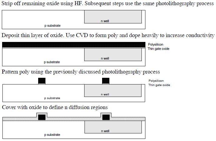
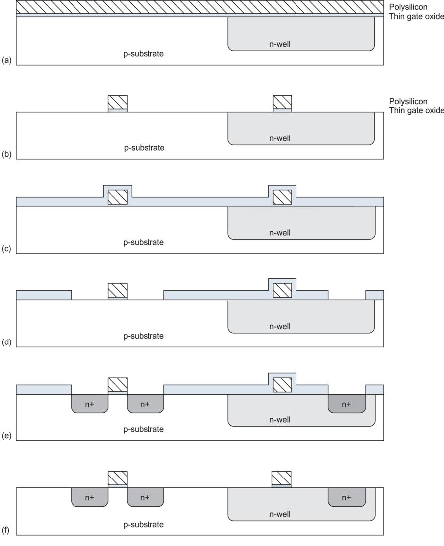
33 Start with blank wafer First step will be to form the n-well Cover wafer with protective layer of SiO2 (oxide) Remove layer where n-well should be built Implant or diffuse n dopants into exposed wafer Strip off SiO2 33
34 34
35 35
36 Fabrication Steps Start with blank wafer Build inverter from the bottom up First step will be to form the n-well Cover wafer with protective layer of SiO2 (oxide) Remove layer where n-well should be built Implant or diffuse n dopants into exposed wafer Strip off SiO2 p substrate 36
37 Oxidation Grow SiO2 on top of Si wafer C with H2O or O2 in oxidation furnace SiO 2 p substrate 37
38 Photoresist Spin on photoresist Photoresist is a light-sensitive organic polymer Softens where exposed to light Photoresist SiO 2 p substrate 38
39 Lithography Expose photoresist through n-well mask Strip off exposed photoresist Photoresist SiO 2 p substrate 39
40 Etch Etch oxide with hydrofluoric acid (HF) Seeps through skin and eats bone; nasty stuff!!! Only attacks oxide where resist has been exposed Photoresist SiO 2 p substrate 40
41 Strip Photoresist Strip off remaining photoresist Use mixture of acids called piranah etch Necessary so resist doesn t melt in next step SiO 2 p substrate 41
42 n-well n-well is formed with diffusion or ion implantation Diffusion Place wafer in furnace with arsenic gas Heat until As atoms diffuse into exposed Si Ion Implanatation Blast wafer with beam of As ions Ions blocked by SiO2, only enter exposed Si SiO 2 n well 42
43 Strip Oxide Strip off the remaining oxide using HF Back to bare wafer with n-well Subsequent steps involve similar series of steps p substrate n well 43
44 Polysilicon Deposit very thin layer of gate oxide < 20 Å (6-7 atomic layers) Chemical Vapor Deposition (CVD) of silicon layer Place wafer in furnace with Silane gas (SiH4) Forms many small crystals called polysilicon Heavily doped to be good conductor Polysilicon Thin gate oxide p substrate n well 44
45 Polysilicon Patterning Use same lithography process to pattern polysilicon Polysilicon Polysilicon Thin gate oxide p substrate n well 45
46 Self-Aligned Process Use oxide and masking to expose where n+ dopants should be diffused or implanted N-diffusion forms nmos source, drain, and n-well contact p substrate n well 46
47 N-diffusion Pattern oxide and form n+ regions Self-aligned process where gate blocks diffusion Polysilicon is better than metal for self-aligned gates because it doesn t melt during later processing n+ Diffusion p substrate n well 47
48 N-diffusion Historically dopants were diffused Usually ion implantation today But regions are still called diffusion n+ n+ n+ p substrate n well 48
49 N-diffusion Strip off oxide to complete patterning step n+ n+ n+ p substrate n well 49
50 P-Diffusion Similar set of steps form p+ diffusion regions for pmos source and drain and substrate contact p+ Diffusion p+ n+ n+ p+ p+ n+ p substrate n well 50
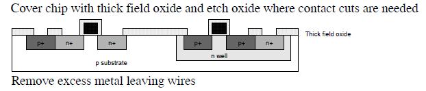
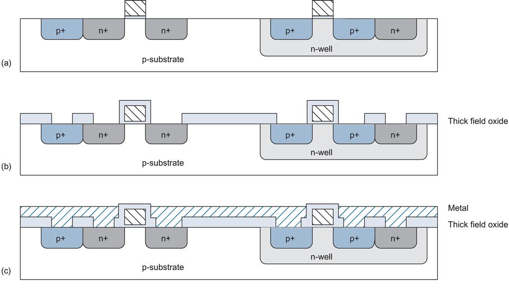
51 Contacts Now we need to wire together the devices Cover chip with thick field oxide Etch oxide where contact cuts are needed Contact p+ n+ n+ p+ p+ n+ Thick field oxide p substrate n well 51
52 Metallization Sputter on aluminum over whole wafer Pattern to remove excess metal, leaving wires Metal p+ n+ n+ p+ p+ n+ Metal Thick field oxide p substrate n well 52
53 Twin-Tub (Twin-Well) CMOS Process This technology provides the basis for separate optimization of the nmos and pmos transistors, thus making it possible for threshold voltage, body effect and the channel transconductance of both types of transistors to be tuned independently. Generally, the starting material is a n+ or p+ substrate, with a lightly doped epitaxial layer on top. This epitaxial layer provides the actual substrate on which the n-well and the p-well are formed. Since two independent doping steps are performed for the creation of the well regions, the dopant concentrations can be carefully optimized to produce the desired device characteristics. The Twin-Tub process is shown below. In the conventional p & n-well CMOS process, the doping density of the well region is typically about one order of magnitude higher than the substrate, which, among other effects, results in unbalanced drain parasitics. The twin-tub process avoids this problem. 53
54 Advanced CMOS Technologies For inexpensive and low-performance chips, one may use a heavily doped substrate and omit one well. The substrate should be doped to about /cm 3, with a resistivity of about 1 Ω-cm. This allows simpler construction, with good Ground Potential distribution, but the devices are not optimal and there is a chance of latch-up if the voltages are pushed hard. For high-performance chips, one uses a low doped substrate, /cm 3, 10 Ω-cm, and then constructs Two Wells at optimum doping levels (called Tubs in the diagram). Since the substrate is lightly doped, there is less chance for latch-up because of the high resistivity. Substrate for Twin-Well MOS Technogy
55 Self-aligned Twin Well 55 Wafer clean Grow pad oxide Deposit nitride (a) N-well mask Etch nitride Strip photoresist N-well implantation (b) Anneal/drive-in and oxidation (c) Strip nitride P-well implantation (d) Anneal and drive Strip pad oxide (e) (a) (b) (c) (d) (e) Silicon Phosphorus Ions Silicon Silicon Dioxide N-well Silicon Silicon Dioxide N-well Silicon N-well Silicon Nitride Nitride Nitride Boron Ion Implantation P-well
56 Self-aligned Twin Well Advantage: reduce a photo mask step Reduce cost Improve IC chip yield. Disadvantage: wafer surface is not flat n-well always has lower level than p-well Affect photolithography resolution Affect thin film deposition N-well implant first Phosphorus diffuses slower than boron in single silicon If p-well implant first, boron in p-well could diffuse out of control during n-well anneal and drive-in 56
57 Twin Well Two mask steps Flat surface Common used in advanced CMOS IC chip High energy, low current implanters Furnaces annealing and driving-in Phosphorus Ions Boron Ions Photoresist P-Epi N-Well P-Well Photoresist N-Well P-Wafer P-Epi P-Wafer 57
58 Silicon-on-Insulator (SOI) CMOS Process Rather than using silicon as the substrate material, technologists have sought to use an insulating substrate to improve process characteristics such as speed and latch-up susceptibility. The SOI CMOS technology allows the creation of independent, completely isolated nmos and pmos transistors virtually side-by-side on an insulating substrate. The main advantages of this technology are the higher integration density (because of the absence of well regions), complete avoidance of the latch-up problem, and lower parasitic capacitances compared to the conventional p & n-well or twin-tub CMOS processes. A cross-section of nmos and pmos devices using SOI process is shown below. The SOI CMOS process is considerably more costly than the standard p & n-well CMOS process. Yet the improvements of device performance and the absence of latch-up problems can justify its use, especially for deep-sub-micron devices. 58

59 Thank you
Introduction to CMOS VLSI Design. Layout, Fabrication, and Elementary Logic Design
 Introduction to CMOS VLSI Design Layout, Fabrication, and Elementary Logic Design CMOS Fabrication CMOS transistors are fabricated on silicon wafer Lithography process similar to printing press On each
CMOS Fabrication. Dr. Bassam Jamil. Adopted from slides of the textbook
 CMOS Fabrication Dr. Bassam Jamil Adopted from slides of the textbook CMOS Fabrication CMOS transistors are fabricated on silicon wafer Lithography process similar to printing press On each step, different
Lecture 0: Introduction
 Lecture 0: Introduction Introduction Integrated circuits: many transistors on one chip. Very Large Scale Integration (VLSI): bucketloads! Complementary Metal Oxide Semiconductor Fast, cheap, low power
UT Austin, ECE Department VLSI Design 2. CMOS Fabrication, Layout Rules
 2. CMOS Fabrication, Layout, Design Rules Last module: Introduction to the course How a transistor works CMOS transistors This module: CMOS Fabrication Design Rules CMOS Fabrication CMOS transistors are
VLSI. Lecture 1. Jaeyong Chung System-on-Chips (SoC) Laboratory Incheon National University. Based on slides of David Money Harris
 Laboratory Incheon National University. Based on slides of David Money Harris") VLSI Lecture 1 Jaeyong Chung System-on-Chips (SoC) Laboratory Incheon National University Based on slides of David Money Harris Goals of This Course Learn the principles of VLSI design Learn to design
VLSI Lecture 1 Jaeyong Chung System-on-Chips (SoC) Laboratory Incheon National University Based on slides of David Money Harris Goals of This Course Learn the principles of VLSI design Learn to design
FABRICATION OF CMOS INTEGRATED CIRCUITS. Dr. Mohammed M. Farag
 FABRICATION OF CMOS INTEGRATED CIRCUITS Dr. Mohammed M. Farag Outline Overview of CMOS Fabrication Processes The CMOS Fabrication Process Flow Design Rules EE 432 VLSI Modeling and Design 2 CMOS Fabrication
PROCESS FLOW AN INSIGHT INTO CMOS FABRICATION PROCESS
 Contents: VI Sem ECE 06EC63: Analog and Mixed Mode VLSI Design PROCESS FLOW AN INSIGHT INTO CMOS FABRICATION PROCESS 1. Introduction 2. CMOS Fabrication 3. Simplified View of Fabrication Process 3.1 Alternative
CMOS VLSI Design. Introduction. All materials are from the textbook Weste and Harris, 3 rd Edition CMOS VLSI DESIGN. Introduction
 CMOS VLSI Design Introduction ll materials are from the textbook Weste and Harris, 3 rd Edition CMOS VLSI DESIGN Introduction Chapter previews the entire field, subsequent chapters elaborate on specific
Lecture 1A: Manufacturing& Layout
 Introduction to CMOS VLSI Design Lecture 1A: Manufacturing& Layout David Harris Harvey Mudd College Spring 2004 Steven Levitan Fall 2008 1 The Manufacturing Process For a great tour through the IC manufacturing
Fabrication and Layout
 ECEN454 Digital Integrated Circuit Design Fabrication and Layout ECEN 454 3.1 A Glimpse at MOS Device Polysilicon Aluminum ECEN 475 4.2 1 Material Classification Insulators Glass, diamond, silicon oxide
Lecture 2: CMOS Fabrication Mark McDermott Electrical and Computer Engineering The University of Texas at Austin
 Lecture 2: CMOS Fabrication Mark McDermott Electrical and Computer Engineering The University of Texas at Austin Agenda Last module: Introduction to the course How a transistor works CMOS transistors This
CMOS FABRICATION. n WELL PROCESS
 CMOS FABRICATION n WELL PROCESS Step 1: Si Substrate Start with p- type substrate p substrate Step 2: Oxidation Exposing to high-purity oxygen and hydrogen at approx. 1000 o C in oxidation furnace SiO
Chapter 2 MOS Fabrication Technology
 Chapter 2 MOS Fabrication Technology Abstract This chapter is concerned with the fabrication of metal oxide semiconductor (MOS) technology. Various processes such as wafer fabrication, oxidation, mask
Low Power VLSI Circuits and Systems Prof. Ajit Pal Department of Computer Science and Engineering Indian Institute of Technology, Kharagpur
 Low Power VLSI Circuits and Systems Prof. Ajit Pal Department of Computer Science and Engineering Indian Institute of Technology, Kharagpur Lecture No. # 02 MOS Transistors - I Hello and welcome to today
VLSI Technology. By: Ajay Kumar Gautam
 By: Ajay Kumar Gautam Introduction to VLSI Technology, Crystal Growth, Oxidation, Epitaxial Process, Diffusion Process, Ion Implantation, Lithography, Etching, Metallization, VLSI Process Integration,
CHAPTER - 4 CMOS PROCESSING TECHNOLOGY
 CHAPTER - 4 CMOS PROCESSING TECHNOLOGY Samir kamal Spring 2018 4.1 CHAPTER OBJECTIVES 1. Introduce the CMOS designer to the technology that is responsible for the semiconductor devices that might be designed
Chapter 3 CMOS processing technology
 Chapter 3 CMOS processing technology (How to make a CMOS?) Si + impurity acceptors(p-type) donors (n-type) p-type + n-type => pn junction (I-V) 3.1.1 (Wafer) Wafer = A disk of silicon (0.25 mm - 1 mm thick),
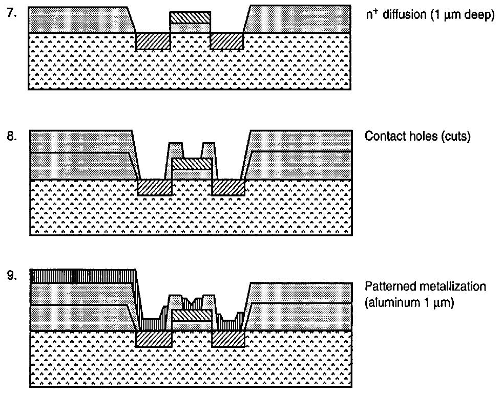
Chapter 2 Problems. The CMOS technology we need to realize is shown below, from Figure 1-34 in the text. S P + N P + N WELL P +
 Chapter 2 roblems 2.1 Sketch a process flow that would result in the structure shown in Figure 1-34 by drawing a series of drawings similar to those in this chapter. You only need to describe the flow
CS/ECE 5710/6710. N-type Transistor. N-type from the top. Diffusion Mask. Polysilicon Mask. CMOS Processing
 CS/ECE 5710/6710 CMOS Processing Addison-Wesley N-type Transistor D G +Vgs + Vds S N-type from the top i electrons - Diffusion Mask Mask for just the diffused regions Top view shows patterns that make
Chapter 2 Manufacturing Process
 Digital Integrated Circuits A Design Perspective Chapter 2 Manufacturing Process 1 CMOS Process 2 CMOS Process (n-well) Both NMOS and PMOS must be built in the same silicon material. PMOS in n-well NMOS
EE 330 Lecture 9. IC Fabrication Technology Part II. -Oxidation -Epitaxy -Polysilicon -Planarization -Resistance and Capacitance in Interconnects
 EE 330 Lecture 9 IC Fabrication Technology Part II -Oxidation -Epitaxy -Polysilicon -Planarization -Resistance and Capacitance in Interconnects Review from Last Time IC Fabrication Technology Crystal Preparation
CMOS Technology. Flow varies with process types & company. Start with substrate selection. N-Well CMOS Twin-Well CMOS STI
 CMOS Technology Flow varies with process types & company N-Well CMOS Twin-Well CMOS STI Start with substrate selection Type: n or p Doping level, resistivity Orientation, 100, or 101, etc Other parameters
EE 330 Lecture 8. IC Fabrication Technology Part II. - Oxidation - Epitaxy - Polysilicon - Interconnects
 EE 330 Lecture 8 IC Fabrication Technology Part II - Oxidation - Epitaxy - Polysilicon - Interconnects Review from Last Time MOS Transistor Bulk Source Gate Drain p-channel MOSFET Lightly-doped n-type
EE 330 Lecture 9. IC Fabrication Technology Part 2
 EE 330 Lecture 9 IC Fabrication Technology Part 2 Quiz 8 A 2m silicon crystal is cut into wafers using a wire saw. If the wire diameter is 220um and the wafer thickness is 350um, how many wafers will this
Department of Electrical Engineering. Jungli, Taiwan
 Chapter 3 Fabrication of CMOS Integrated Circuits Jin-Fu Li Department of Electrical Engineering National Central University Jungli, Taiwan Background Outline The CMOS Process Flow Design Rules Latchup
Microfabrication of Integrated Circuits
 Microfabrication of Integrated Circuits OUTLINE History Basic Processes Implant; Oxidation; Photolithography; Masks Layout and Process Flow Device Cross Section Evolution Lecture 38, 12/05/05 Reading This
Lecture 19 Microfabrication 4/1/03 Prof. Andy Neureuther
 EECS 40 Spring 2003 Lecture 19 Microfabrication 4/1/03 Prof. ndy Neureuther How are Integrated Circuits made? Silicon wafers Oxide formation by growth or deposition Other films Pattern transfer by lithography
Complexity of IC Metallization. Early 21 st Century IC Technology
 EECS 42 Introduction to Digital Electronics Lecture # 25 Microfabrication Handout of This Lecture. Today: how are Integrated Circuits made? Silicon wafers Oxide formation by growth or deposition Other
EE40 Lec 22. IC Fabrication Technology. Prof. Nathan Cheung 11/19/2009
 Suggested Reading EE40 Lec 22 IC Fabrication Technology Prof. Nathan Cheung 11/19/2009 300mm Fab Tour http://www-03.ibm.com/technology/manufacturing/technology_tour_300mm_foundry.html Overview of IC Technology
This Appendix discusses the main IC fabrication processes.
 IC Fabrication B B.1 Introduction This Appendix discusses the main IC fabrication processes. B.2 NMOS fabrication NMOS transistors are formed in a p-type substrate. The NMOS fabrication process requires
Ajay Kumar Gautam [VLSI TECHNOLOGY] VLSI Technology for 3RD Year ECE/EEE Uttarakhand Technical University
![Ajay Kumar Gautam [VLSI TECHNOLOGY] VLSI Technology for 3RD Year ECE/EEE Uttarakhand Technical University](/thumbs/75/72824557.jpg "Ajay Kumar Gautam [VLSI TECHNOLOGY] VLSI Technology for 3RD Year ECE/EEE Uttarakhand Technical University") 2014 Ajay Kumar Gautam [VLSI TECHNOLOGY] VLSI Technology for 3RD Year ECE/EEE Uttarakhand Technical University Page1 Syllabus UNIT 1 Introduction to VLSI Technology: Classification of ICs, Scale of integration,
2014 Ajay Kumar Gautam [VLSI TECHNOLOGY] VLSI Technology for 3RD Year ECE/EEE Uttarakhand Technical University Page1 Syllabus UNIT 1 Introduction to VLSI Technology: Classification of ICs, Scale of integration,
9/4/2008 GMU, ECE 680 Physical VLSI Design
 ECE680: Physical VLSI Design Chapter II CMOS Manufacturing Process 1 Dual-Well Trench-Isolated CMOS Process gate-oxide TiSi 2 AlCu Tungsten SiO 2 p-well poly n-well SiO 2 n+ p-epi p+ p+ 2 Schematic Layout
FABRICATION of MOSFETs
 FABRICATION of MOSFETs CMOS fabrication sequence -p-type silicon substrate wafer -creation of n-well regions for pmos transistors, -impurity implantation into the substrate. -thick oxide is grown in the
EEC 118 Lecture #5: MOS Fabrication. Rajeevan Amirtharajah University of California, Davis Jeff Parkhurst Intel Corporation
 EEC 118 Lecture #5: MOS Fabrication Rajeevan Amirtharajah University of California, Davis Jeff Parkhurst Intel Corporation Announcements Lab 3 this week, report due next week HW 3 due this Friday at 4
Manufacturing Process
 Manufacturing Process 1 CMOS Process 2 A Modern CMOS Process gate-oxide TiSi 2 AlCu Tungsten SiO 2 n+ p-well p-epi poly n-well p+ SiO 2 p+ Dual-Well Trench-Isolated CMOS Process 3 Single-crystal ingot
Lecture 030 Integrated Circuit Technology - I (5/8/03) Page 030-1
 Page 030-1") Lecture 030 Integrated Circuit Technology - I (5/8/03) Page 030-1 LECTURE 030 INTEGRATED CIRCUIT TECHNOLOGY - I (References [7,8]) Objective The objective of this presentation is: 1.) Illustrate integrated
Lecture 030 Integrated Circuit Technology - I (5/8/03) Page 030-1 LECTURE 030 INTEGRATED CIRCUIT TECHNOLOGY - I (References [7,8]) Objective The objective of this presentation is: 1.) Illustrate integrated
EE 434 Lecture 9. IC Fabrication Technology
 EE 434 Lecture 9 IC Fabrication Technology Quiz 7 The layout of a film resistor with electrodes A and B is shown. If the sheet resistance of the film is 40 /, determine the resistance between nodes A and
Complementary Metal-Oxide-Semiconductor Very Large-Scale Integrated Circuit Design
 Complementary Metal-Oxide-Semiconductor Very Large-Scale Integrated Circuit Design Bradley A. Minch Mixed Analog-Digital VLSI Circuits and Systems Lab Cornell University Ithaca, NY 14853 5401 minch@ece.cornell.edu
UNIT 4. By: Ajay Kumar Gautam Asst. Prof. Dev Bhoomi Institute of Technology & Engineering, Dehradun
 UNIT 4 By: Ajay Kumar Gautam Asst. Prof. Dev Bhoomi Institute of Technology & Engineering, Dehradun Syllabus METALLIZATION: Applications and choices, physical vapor deposition, patterning, problem areas.
Microelectronics. Integrated circuits. Introduction to the IC technology M.Rencz 11 September, Expected decrease in line width
 Microelectronics Introduction to the IC technology M.Rencz 11 September, 2002 9/16/02 1/37 Integrated circuits Development is controlled by the roadmaps. Self-fulfilling predictions for the tendencies
EECS130 Integrated Circuit Devices
 EECS130 Integrated Circuit Devices Professor Ali Javey 9/13/2007 Fabrication Technology Lecture 1 Silicon Device Fabrication Technology Over 10 15 transistors (or 100,000 for every person in the world)
Fabrication and Layout
 Fabrication and Layout Kenneth Yun UC San Diego Adapted from EE271 notes, Stanford University Overview Semiconductor properties How chips are made Design rules for layout Reading Fabrication: W&E 3.1,
HOMEWORK 4 and 5. March 15, Homework is due on Monday March 30, 2009 in Class. Answer the following questions from the Course Textbook:
 HOMEWORK 4 and 5 March 15, 2009 Homework is due on Monday March 30, 2009 in Class. Chapter 7 Answer the following questions from the Course Textbook: 7.2, 7.3, 7.4, 7.5, 7.6*, 7.7, 7.9*, 7.10*, 7.16, 7.17*,
EE 330 Lecture 8. IC Fabrication Technology Part II. - Masking - Photolithography - Deposition - Etching - Diffusion
 EE 330 Lecture 8 IC Fabrication Technology Part II?? - Masking - Photolithography - Deposition - Etching - Diffusion Review from Last Time Technology Files Provide Information About Process Process Flow
Silicon Wafer Processing PAKAGING AND TEST
 Silicon Wafer Processing PAKAGING AND TEST Parametrical test using test structures regularly distributed in the wafer Wafer die test marking defective dies dies separation die fixing (not marked as defective)
Figure 2.3 (cont., p. 60) (e) Block diagram of Pentium 4 processor with 42 million transistors (2000). [Courtesy Intel Corporation.
 (e) Block diagram of Pentium 4 processor with 42 million transistors (2000). [Courtesy Intel Corporation.") Figure 2.1 (p. 58) Basic fabrication steps in the silicon planar process: (a) oxide formation, (b) selective oxide removal, (c) deposition of dopant atoms on wafer, (d) diffusion of dopant atoms into exposed
Figure 2.1 (p. 58) Basic fabrication steps in the silicon planar process: (a) oxide formation, (b) selective oxide removal, (c) deposition of dopant atoms on wafer, (d) diffusion of dopant atoms into exposed
Fabrication Technology
 Fabrication Technology By B.G.Balagangadhar Department of Electronics and Communication Ghousia College of Engineering, Ramanagaram 1 OUTLINE Introduction Why Silicon The purity of Silicon Czochralski
VLSI Digital Systems Design
 VLSI Digital Systems Design CMOS Processing cmpe222_03process_ppt.ppt 1 Si Purification Chemical purification of Si Zone refined Induction furnace Si ingot melted in localized zone Molten zone moved from
The Physical Structure (NMOS)
") The Physical Structure (NMOS) Al SiO2 Field Oxide Gate oxide S n+ Polysilicon Gate Al SiO2 SiO2 D n+ L channel P Substrate Field Oxide contact Metal (S) n+ (G) L W n+ (D) Poly 1 3D Perspective 2 3 Fabrication
The Physical Structure (NMOS) Al SiO2 Field Oxide Gate oxide S n+ Polysilicon Gate Al SiO2 SiO2 D n+ L channel P Substrate Field Oxide contact Metal (S) n+ (G) L W n+ (D) Poly 1 3D Perspective 2 3 Fabrication
Lecture #18 Fabrication OUTLINE
 Transistors on a Chip Lecture #18 Fabrication OUTLINE IC Fabrication Technology Introduction the task at hand Doping Oxidation Thin-film deposition Lithography Etch Lithography trends Plasma processing
EE 560 FABRICATION OF MOS CIRCUITS. Kenneth R. Laker, University of Pennsylvania
 1 EE 560 FABRICATION OF MOS CIRCUITS 2 CMOS CHIP MANUFACTRING STEPS Substrate Wafer Wafer Fabrication (diffusion, oxidation, photomasking, ion implantation, thin film deposition, etc.) Finished Wafer Wafer
EE 330 Lecture 9. IC Fabrication Technology Part II. -Oxidation -Epitaxy -Polysilicon -Planarization -Resistance and Capacitance in Interconnects
 EE 330 Lecture 9 IC Fabrication Technology Part II -Oxidation -Epitaxy -Polysilicon -Planarization -Resistance and Capacitance in Interconnects Review from Last Time Etching Dry etch (anisotropic) SiO
Fabrication Process. Crystal Growth Doping Deposition Patterning Lithography Oxidation Ion Implementation CONCORDIA VLSI DESIGN LAB
 Fabrication Process Crystal Growth Doping Deposition Patterning Lithography Oxidation Ion Implementation 1 Fabrication- CMOS Process Starting Material Preparation 1. Produce Metallurgical Grade Silicon
We are moving to 155 Donner Lab From Thursday, Feb 2 We will be able to accommodate everyone!
 -Spring 006 Digital Integrated Circuits Lecture 4 CMOS Manufacturing Process Design Rules EECS141 1 Good News! We are moving to 155 Donner Lab From Thursday, Feb We will be able to accommodate everyone!
CMOS Processing Technology
 CHAPTER 2 CMOS Processing Technology Outline 2 1. CMOS Technologies 2. Layout Design Rules 3. CMOS Process Enhancements 4. Technology-related CAD Issues 5. Manufacturing Issues CMOS Technologies 3 n-well
Integrated Circuits & Systems
 Federal University of Santa Catarina Center for Technology Computer Science & Electronics Engineering Integrated Circuits & Systems INE 5442 Lecture 6 CMOS Fabrication Process & Design Rules guntzel@inf.ufsc.br
CMOS Manufacturing process. Design rule set
 CMOS Manufacturing process Circuit design Set of optical masks Fabrication process Circuit designer Design rule set Process engineer All material: Chap. 2 of J. Rabaey, A. Chandrakasan, B. Nikolic, Digital
Czochralski Crystal Growth
 Czochralski Crystal Growth Crystal Pulling Crystal Ingots Shaping and Polishing 300 mm wafer 1 2 Advantage of larger diameter wafers Wafer area larger Chip area larger 3 4 Large-Diameter Wafer Handling
CMOS Manufacturing process. Circuit designer. Design rule set. Process engineer. Set of optical masks. Fabrication process.
 CMOS Manufacturing process Circuit design Set of optical masks Fabrication process Circuit designer Design rule set Process engineer All material: Chap. 2 of J. Rabaey, A. Chandrakasan, B. Nikolic, Digital
EE 143 FINAL EXAM NAME C. Nguyen May 10, Signature:
 INSTRUCTIONS Read all of the instructions and all of the questions before beginning the exam. There are 5 problems on this Final Exam, totaling 143 points. The tentative credit for each part is given to
conductor - gate insulator source gate n substrate conductor - gate insulator gate substrate n open switch closed switch however: closed however:
 MOS Transistors Readings: Chapter 1 N-type drain conductor - gate insulator source gate drain source n p n substrate P-type drain conductor - gate insulator source drain gate source p p substrate n 42
Manufacturing Process
 Digital Integrated Circuits A Design Perspective Jan M. Rabaey Anantha Chandrakasan Borivoje Nikolic Manufacturing Process July 30, 2002 1 CMOS Process 2 A Modern CMOS Process gate-oxide TiSi 2 AlCu Tungsten
Fairchild Semiconductor Application Note June 1983 Revised March 2003
 Fairchild Semiconductor Application Note June 1983 Revised March 2003 High-Speed CMOS (MM74HC) Processing The MM74HC logic family achieves its high speed by utilizing microcmos Technology. This is a 3.5
CMOS Processing Technology
 CHAPTER 2 CMOS Processing Technology Outline 2 1. CMOS Technologies 2. Layout Design Rules 3. CMOS Process Enhancements 4. Technology-related CAD Issues 5. Manufacturing Issues CMOS Technologies 3 n-well
TOWARD MEMS!Instructor: Riadh W. Y. Habash
 TOWARD MEMS!Instructor: Riadh W. Y. Habash Students are presented with aspects of general production and manufacturing of integrated circuit (IC) products to enable them to better liaise with and participate
ECE 659. Jan M. Rabaey Anantha Chandrakasan Borivoje Nikolic. July 30, Digital EE141 Integrated Circuits 2nd Manufacturing.
 Digital Integrated Circuits A Design Perspective Jan M. Rabaey Anantha Chandrakasan Borivoje Nikolic Manufacturing Process July 0, 00 1 CMOS Process 1 A Modern CMOS Process gate-oxide TiSi AlCu Tungsten
VLSI Technology Dr. Nandita Dasgupta Department of Electrical Engineering Indian Institute of Technology, Madras
 VLSI Technology Dr. Nandita Dasgupta Department of Electrical Engineering Indian Institute of Technology, Madras Lecture - 36 MOSFET I Metal gate vs self-aligned poly gate So far, we have discussed about
VLSI Design and Simulation
 VLSI Design and Simulation CMOS Processing Technology Topics CMOS Processing Technology Semiconductor Processing How do we make a transistor? Fabrication Process Wafer Processing Silicon single crystal
MOS Front-End. Field effect transistor
 MOS Front-End Back-end Transistor Contact Front-end p-well STI n-well Front-end-of-line includes substrate, isolation, wells, transistor, silicide Field effect transistor MOSFET: Metal-Oxide-Semiconductor
ECE520 VLSI Design. Lecture 7: CMOS Manufacturing Process. Payman Zarkesh-Ha
 ECE520 VLSI Design Lecture 7: CMOS Manufacturing Process Payman Zarkesh-Ha Office: ECE Bldg. 230B Office hours: Wednesday 2:00-3:00PM or by appointment E-mail: pzarkesh@unm.edu Slide: 1 Review of Last
EE 5611 Introduction to Microelectronic Technologies Fall Tuesday, September 04, 2012 Lecture 01
 EE 5611 Introduction to Microelectronic Technologies Fall 2012 Tuesday, September 04, 2012 Lecture 01 1 Instructor: Jing Bai Contact Email: jingbai@d.umn.edu, hone: (218)726-8606, Office: MWAH 255 Webpage:
Process Flow in Cross Sections
 Process Flow in Cross Sections Process (simplified) 0. Clean wafer in nasty acids (HF, HNO 3, H 2 SO 4,...) --> wear gloves! 1. Grow 500 nm of SiO 2 (by putting the wafer in a furnace with O 2 2. Coat
Manufacturing Process
 CMOS Manufacturing Process CMOS Process 1 A Modern CMOS Process gate-oxide TiSi AlCu Tungsten SiO n+ p-well p-epi poly n-well p+ SiO p+ Dual-Well Trench-Isolated CMOS Process Circuit Under Design V DD
EE6303 LINEAR INTEGRATED CIRCUITS AND APPLICATIONS 2 MARK QUESTIONS WITH ANSWERS UNIT I IC FABRICATION
 SRI VENKATESWARA COLLEGE OF ENGINEERING AND TECHNOLOGY TIRUPACHUR DEPARTMENT OFELECTRICAL AND ELECTRONICS ENGINEERING EE6303 LINEAR INTEGRATED CIRCUITS AND APPLICATIONS 1. Define an Integrated circuit.
Lecture 22: Integrated circuit fabrication
 Lecture 22: Integrated circuit fabrication Contents 1 Introduction 1 2 Layering 4 3 Patterning 7 4 Doping 8 4.1 Thermal diffusion......................... 10 4.2 Ion implantation.........................
CMOS Manufacturing Process
 CMOS Manufacturing Process CMOS Process A Modern CMOS Process gate-oxide TiSi 2 AlCu Tungsten SiO 2 n+ p-well p-epi poly n-well p+ SiO 2 p+ Dual-Well Trench-Isolated CMOS Process Circuit Under Design V
EE 5611 Introduction to Microelectronic Technologies Fall Tuesday, September 02, 2014 Lecture 01
 EE 5611 Introduction to Microelectronic Technologies Fall 2014 Tuesday, September 02, 2014 Lecture 01 1 Instructor: Jing Bai Contact Email: jingbai@d.umn.edu, hone: (218)726-8606, Office: MWAH 255 Webpage:
Chapter 3 Silicon Device Fabrication Technology
 Chapter 3 Silicon Device Fabrication Technology Over 10 15 transistors (or 100,000 for every person in the world) are manufactured every year. VLSI (Very Large Scale Integration) ULSI (Ultra Large Scale
Process Integration. MEMS Release Techniques Sacrificial Layer Removal Substrate Undercut
 Process Integration Self-aligned Techniques LOCOS- self-aligned channel stop Self-aligned Source/Drain Lightly Doped Drain (LDD) Self-aligned silicide (SALICIDE) Self-aligned oxide gap MEMS Release Techniques
Radiation Tolerant Isolation Technology
 Radiation Tolerant Isolation Technology Background The following contains a brief description of isolation technologies used for radiation hardened integrated circuits. The technologies mentioned are junction
Isolation Technology. Dr. Lynn Fuller
 ROCHESTER INSTITUTE OF TECHNOLOGY MICROELECTRONIC ENGINEERING Isolation Technology Dr. Lynn Fuller Motorola Professor 82 Lomb Memorial Drive Rochester, NY 14623-5604 Tel (585) 475-2035 Fax (585) 475-5041
Theory and Technology of Semiconductor Fabrication
 Theory and Technology of Semiconductor Fabrication By Mohammad Razaghi Course description Instructor: Dr. Mohammad Razaghi Assistant Professor Electrical Engineering Department Faculty of Engineering University
Semiconductor Manufacturing Technology. IC Fabrication Process Overview
 Semiconductor Manufacturing Technology Michael Quirk & Julian Serda October 00 by Prentice Hall Chapter 9 IC Fabrication Process Overview /4 Objectives After studying the material in this chapter, you
Chapter 4 : ULSI Process Integration (0.18 m CMOS Process)
") Chapter : ULSI Process Integration (0.8 m CMOS Process) Reference. Semiconductor Manufacturing Technology : Michael Quirk and Julian Serda (00). - (00). Semiconductor Physics and Devices- Basic Principles(/e)
Chapter : ULSI Process Integration (0.8 m CMOS Process) Reference. Semiconductor Manufacturing Technology : Michael Quirk and Julian Serda (00). - (00). Semiconductor Physics and Devices- Basic Principles(/e)
Historical Development. Babbage s second computer. Before the digital age
 Historical Development To fully appreciate the computers of today, it is helpful to understand how things got the way they are The evolution of computing machinery has taken place over several centuries
Semiconductor Physics Course Final Presentation CMOS Fabrication by Özgür Çobanoğlu (Turin, 2006)
") Semiconductor Physics Course Final Presentation CMOS Fabrication by Özgür Çobanoğlu (Turin, 2006) 1 Outline Sections and Contents of the Presentation What is MOS? How does MOS behave in low level? A useful
Semiconductor Physics Course Final Presentation CMOS Fabrication by Özgür Çobanoğlu (Turin, 2006) 1 Outline Sections and Contents of the Presentation What is MOS? How does MOS behave in low level? A useful
Lecture 2. Fabrication and Layout
 Lecture 2 Fabrication and Layout Mark Horowitz Modified by Azita Emami Computer Systems Laboratory Stanford University azita@stanford.edu 1 Overview Reading W&E 3.1(scan), 3.2.1, 3.3.1 - Fabrication W&E
Microelectronics Devices
 Microelectronics Devices Yao-Joe Yang 1 Outline Basic semiconductor physics Semiconductor devices Resistors Capacitors P-N diodes BJT/MOSFET 2 Type of Solid Materials Solid materials may be classified
ASIC Physical Design CMOS Processes
 ASIC Physical Design CMOS Processes Smith Text: Chapters 2 & 3 Weste CMOS VLSI Design Global Foundries: BiCMOS_8HP8XP_Training.pdf BiCMOS_8HP_Design_Manual.pdf Physical design process overview CMOS transistor
Lect. 2: Basics of Si Technology
 Unit processes Thin Film Deposition Etching Ion Implantation Photolithography Chemical Mechanical Polishing 1. Thin Film Deposition Layer of materials ranging from fractions of nanometer to several micro-meters
Process Integration. NMOS Generic NMOS Process Flow. CMOS - The MOSIS Process Flow
 Process Integration Self-aligned Techniques LOCOS- self-aligned channel stop Self-aligned Source/Drain Lightly Doped Drain (LDD) Self-aligned silicide (SALICIDE) Self-aligned oxide gap MEMS Release Techniques
INTEGRATED-CIRCUIT TECHNOLOGY
 INTEGRATED-CIRCUIT TECHNOLOGY 0. Silicon crystal growth and wafer preparation 1. Processing Steps 1.1. Photolitography 1.2. Oxidation 1.3. Layer Deposition 1.4. Etching 1.5. Diffusion 1.6 Backend: assembly,
VLSI Systems and Computer Architecture Lab
 ΚΥΚΛΩΜΑΤΑ VLSI Πανεπιστήμιο Ιωαννίνων CMOS Technology Τμήμα Μηχανικών Η/Υ και Πληροφορικής 1 From the book: An Introduction ti to VLSI Process By: W. Maly ΚΥΚΛΩΜΑΤΑ VLSI Διάρθρωση 1. N well CMOS 2. Active
VLSI Technology Dr. Nandita Dasgupta Department of Electrical Engineering Indian Institute of Technology, Madras
 VLSI Technology Dr. Nandita Dasgupta Department of Electrical Engineering Indian Institute of Technology, Madras Lecture - 33 Problems in LOCOS + Trench Isolation and Selective Epitaxy So, we are discussing
ECE321 Electronics I
 ECE321 Electronics I Lecture 19: CMOS Fabrication Payman Zarkesh-Ha Office: ECE Bldg. 230B Office hours: Tuesday 2:00-3:00PM or by appointment E-mail: payman@ece.unm.edu Slide: 1 Miller Effect Interconnect
Problem 1 Lab Questions ( 20 points total)
") Problem 1 Lab Questions ( 20 points total) (a) (3 points ) In our EE143 lab, we use Phosphorus for the source and drain diffusion. However, most advanced processes use Arsenic. What is the advantage of
Problem 1 Lab Questions ( 20 points total) (a) (3 points ) In our EE143 lab, we use Phosphorus for the source and drain diffusion. However, most advanced processes use Arsenic. What is the advantage of
Schematic creation of MOS field effect transistor.
 Schematic creation of MOS field effect transistor. Gate electrode Drain electrode Source electrode Gate oxide Gate length Page 1 Step 0 The positively doped silicon wafer is first coated with an insulating