Silicon Microfabrication Part 2
|
|
|
- Rhoda Jones
- 6 years ago
- Views:
Transcription


1 Introduction to BioMEMS & Medical Microdevices Silicon Microfabrication Part 2 Companion lecture to the textbook: Fundamentals of BioMEMS and Medical Microdevices, by Prof., R012308
2 Overview Thin-films: Thermal Silicon Oxide Silicon Dioxide (SiO2) Polysilicon Silicon Nitride (Si3N4) Phosphosilicate Glass (PSG) Metal films (e.g. tungsten and aluminum) Thin films may be produced by: Thermal oxidation Physical Vapor Deposition Chemical Vapor Deposition Epitaxial Deposition Atomic Layer Deposition (ADL)
3 Ion implantation to improve electrical conductivity or to control etching characteristics. Wet bulk micromachining Isotropic and anisotropic etching 3-D structure and sacrificial layers Deep Reactive Ion Etching (DRIE) Characterization with Atomic Force Microscopy Substrate bonding Silicon direct bonding Anodic bonding
4 Thin-Films Thin-film application is an additive process. Some important thin-films are: Thermal Silicon Oxide Silicon Dioxide (SiO2) Polysilicon Silicon Nitride (Si3N4) Phosphosilicate Glass (PSG) Metal films (e.g. tungsten and aluminum)
5 Thermal Silicon Oxide Amorphous material. Insulating layer. Mask Sacrificial layer. Impurities such as Na + and K + diffuse through it. Most dopants except Ga diffuse poorly through it. Thicknesses usually less than 1 µm are produced. Silicon Dioxide (SiO2) Chemical Vapor Deposition (CVD) techniques Insulator between conducting layers. Diffusion and ion implantation masks. Sacrificial material.

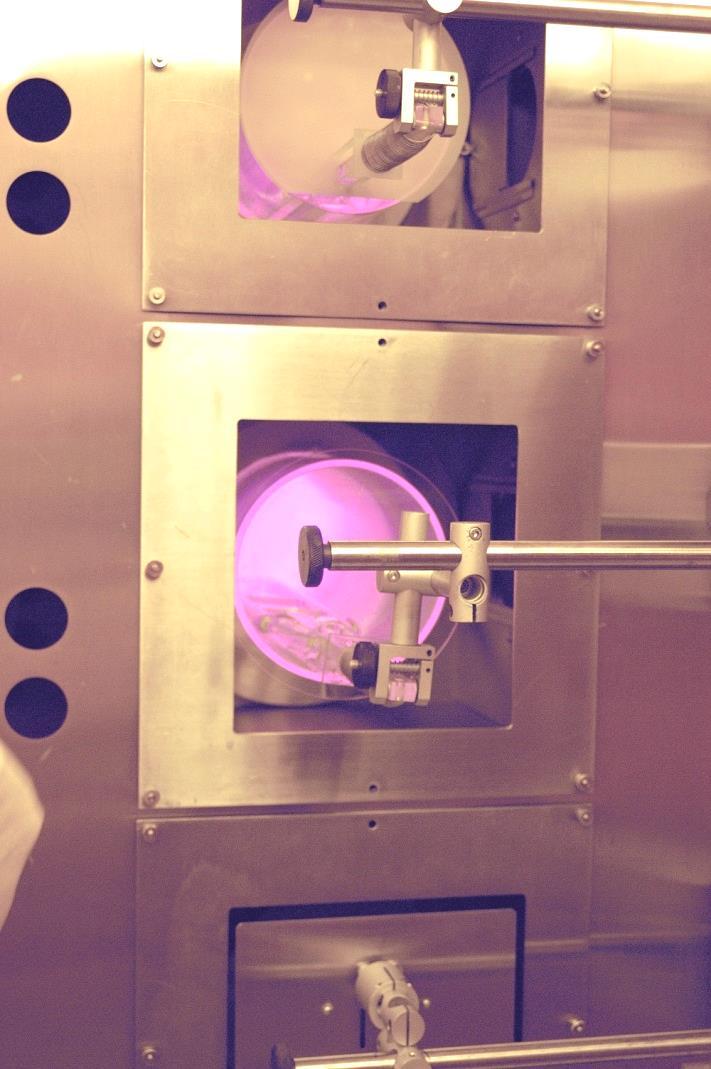
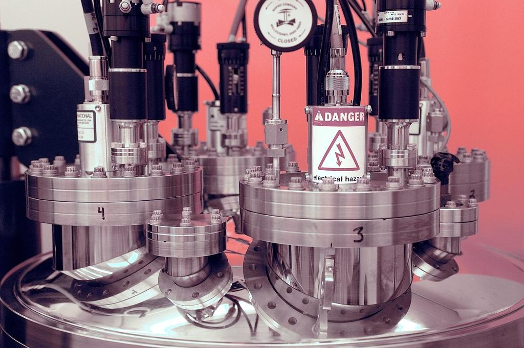
6 Thermal Oxide Furnace
7 Polysilicon Films Low Pressure Chemical Vapor Deposition (LPCVD). Initially amorphous, but may crystallize during deposition. Transition from small grains at the film/substrate interface to columnar crystallites on top. Dopants, impurities and temperature influence crystal orientation. Dopants decrease resistivity to produce conductors and control stress. Can be doped by diffusion, implantation, or by the addition of dopant gases during deposition. Piezoresistive sensor elements may be fabricated from polysilicon.
8 Silicon Nitride (Si 3 N 4 ) CVD Techniques Amorphous Insulator between conducting layers. Excellent water and ionic barrier. Can not be directly put on silicon. May be put on a silicon dioxide layer. Highly selective etch rates. Hard material that may be used for structural purposes. An important mechanical membrane and isolation/buffer material.
9 Phosphosilicate Glass (PSG) PSG and borophosphosilicate glasses (BPSG) soften and flow at lower temperatures, enabling smoothing of topography. Etch faster than silicon dioxide, hence more suitable sacrificial layer. Creating by addition of phosphine to the gas steam. Dielectric between conducting metal layers. Getting and flow capabilities. Passivation coat to provide mechanical protection
10 Metal Films CVD and PVD techniques. Aluminum and tungsten are commonly used. Metals with high reflectivity include Al (aluminum) and Au (gold). Metals with high mass density include W (tungsten), Au (gold) and Pt (platinum). Metals with specific adsorption and adhesion characteristics include Pd (palladium), Ir (iridium), Au (gold) and Pt (platinum). Tungsten will nucleate on silicon or metal surfaces, but not on dielectrics such as oxides and nitrides.
11 Thin-Film Deposition Processes Physical Vapor Deposition Material is transported in vapor form from a source to a substrate through a vacuum or low-pressure gaseous environment: Evaporation, Sputtering, Arc vapor deposition Laser ablation, Ion plating. Chemical Vapor Deposition Chemical vapor deposition is the deposition of a solid on a heated surface from a chemical reaction in the vapor phase. Epitaxial Deposition A single crystal layer can be deposited onto the surface of a substrate wafer.
12 Thermal Evaporation Gardner JW et al, Microsensors, MEMS and Smart Devices, John Wiley & Sons, Chichester, NY (2001)
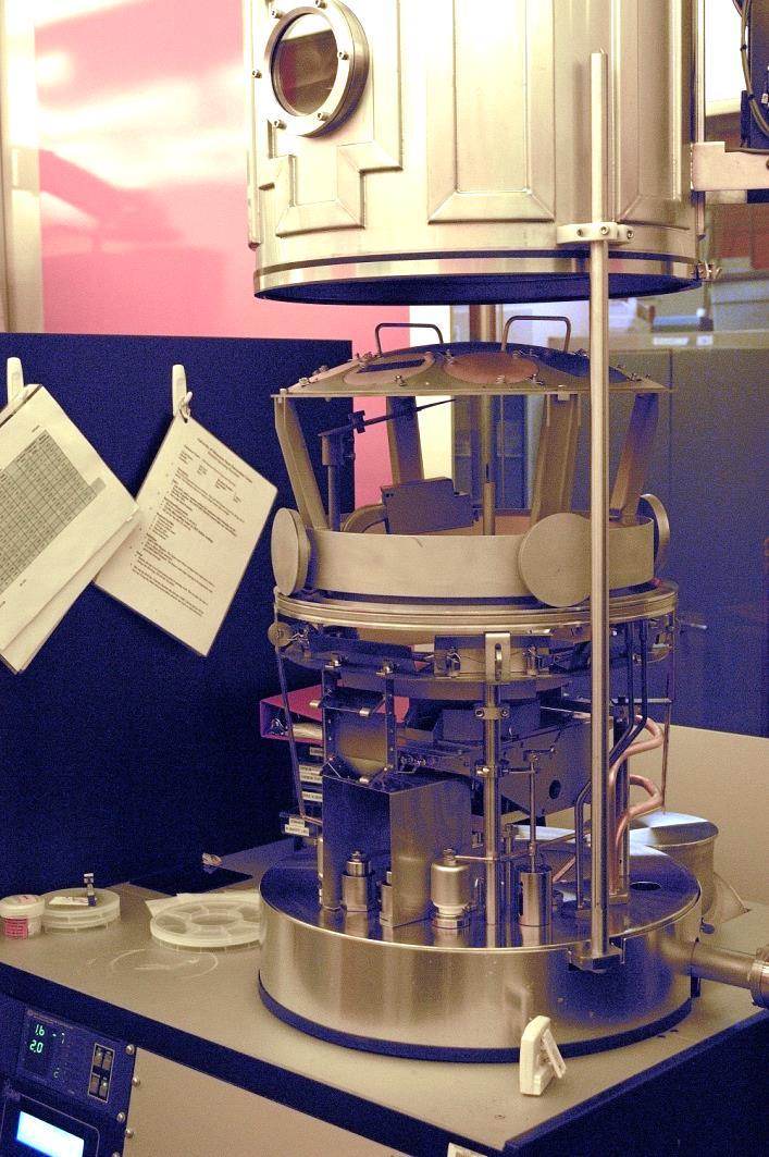
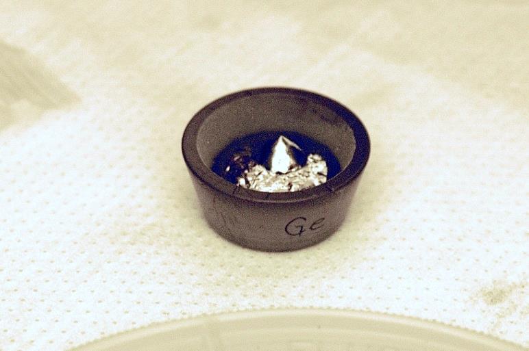
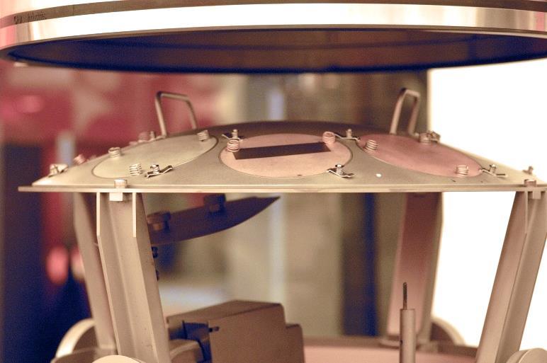
13 E-Beam Evaporator & Crucible
14 Sputter Deposition Brown, R. RF/Microwave Hybrids: Basics, Material and Processes. Kluwer Academic Publishers, Boston (2003.
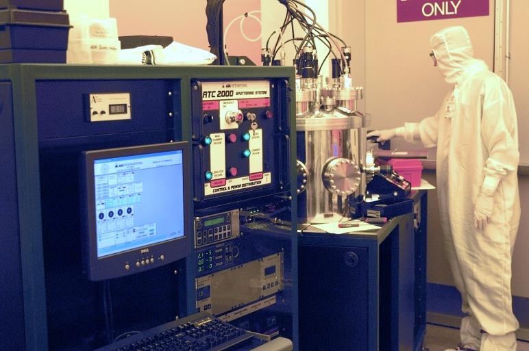
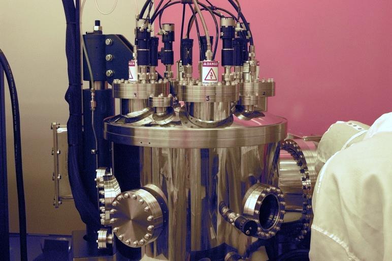
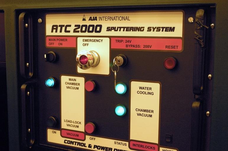
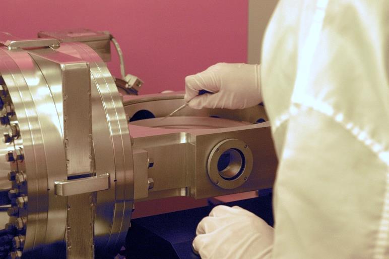
15 Sputtering Equipment
16
17 Chemical Vapor Deposition (CVD) Chemical vapor deposition is the deposition of a solid on a heated surface from a chemical reaction in the vapor phase. Like PVD, the deposition species are atoms or molecules or a combination of these. Advantages & disadvantages
18 Methods Deposition methods. Atmospheric Pressure Chemical Vapor Deposition (APCVD). Low-Pressure Chemical Vapor Deposition (LPCVD). Plasma-enhanced Chemical Vapor Deposition (PECVD). Gardner JW et al, Microsensors, MEMS and Smart Devices, John Wiley & Sons, Chichester, NY (2001)
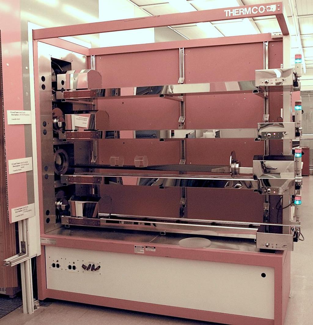
19 LPCVD

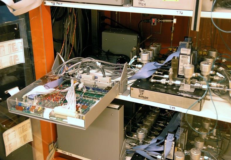
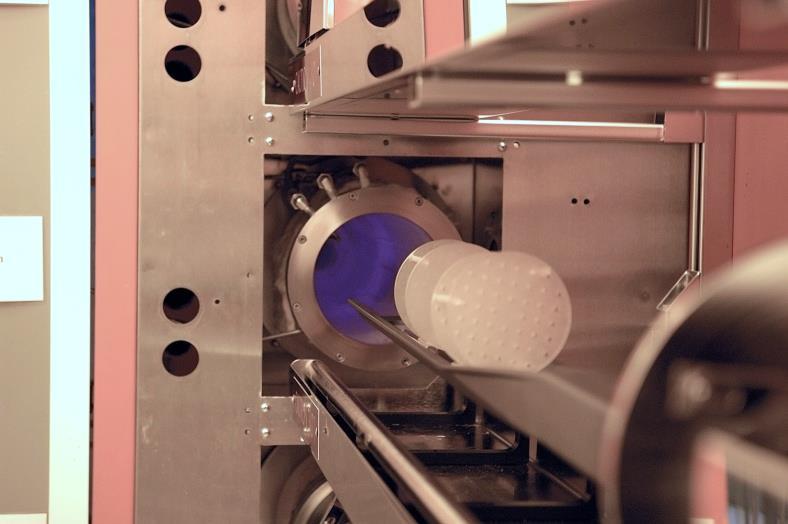
20 Loading the LPCVD
21 CVD Process Pierson HO, Handbook of Chemical Vapor Deposition (CVD): Principles, Technology, and Applications. 2 nd ed. William Andrew Publishing/Noyes, Norwich, N.Y. (1999)
22 Select Thin-Films SiO 2 can be deposited with CVD by reacting silane and oxygen in a LPCVD reactor as shown: 500 C SiH + O SiO + 2H SiO2 can be deposited with LPCVD by decomposing tetra-ethyl-ortho-silicate, Si(OC2H5)4, also known as TEOS. This is vaporized from a liquid source.
23 SiO2 can also be deposited with LPCVD using dichlorosilane: SiCl H + 2H C SiO +2H +2HCl Si3N4 can be deposited with LPCVD using dichlorosilane and ammonia: 3SiCl H + 4NH 800 C Si N + 6HCL + 6H
24 CVD Thin-Film Properties There are three factors that control the nature and properties of the deposit: Epitaxy Gas-phase precipitation Thermal expansion CVD structure can be controlled by manipulation of temperature, pressure, supersaturation and the CVD reaction. Ceramics, including SiO 2, Al 2 O 3, Si 3 N 4 and most dielectrics are amorphous. Metal deposits tend to be crystalline.

25 Atomic Layer Deposition (ALD)

26 Materials That Can Be Deposited Oxides: Al 2 O 3, HfO 2, SiO 2, TiO 2, SrTiO 3, Ta 2 O 5, Gd 2 O 3, ZrO 2, Ga 2 O 3, V 2 O 5, Co 3 O 4, ZnO, ZnO:Al, ZnO:B, In 2 O 3 :H, WO 3, MoO 3, Nb 2 O 5, NiO, MgO, RuO 2 Fluorides: MgF 2, AlF 3 Organic-hybrid materials: Alucone Nitrides: TiN, TaN, Si 3 N 4, AlN, GaN, WN, HfN, NbN, GdN, VN, ZrN Metals: Pt, Ru, Pd, Ni, W Sulfides: ZnS Photo Courtesy of Oxford industries
.")
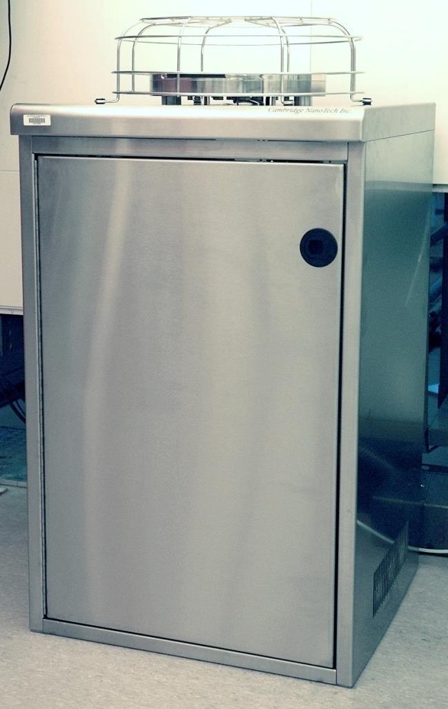
27 Select ALD Features 100% film density guarantees ideal material properties. Insensitive to dust (grows underneath dust!). Oxides, nitrides, metals, semiconductors possible (Cambridge Nanotech provides standard recipes). Amorphous or crystalline depending on substrate and temperature. Cambridge NanoTech Inc.
28 ALD Features Digital thickness control to atomic level (no rate monitor needed, just set the number of atomic layers). Perfect 3D conformality, 100% step coverage: uniform coatings on flat, inside porous and around particle samples. Low defect density. Gentle deposition process for sensitive substrates, no plasma. Low temperature deposition possible (RT-400C). Low stress because of molecular self assembly. Cambridge NanoTech Inc.
29 Ion Implantation 1. In ion implantation, the dopant element is ionized, accelerated to a kinetic energy of several hundred kev, and then driven into the substrate. 2. The electrical conductivity of an intrinsic semiconductor can be increased through doping. The charge carrier density can be increased through impurities of either higher or lower valence. 3. Doping can be used to control etching by reducing etch rates. 4. Sources for n-type doping include antimony, arsenic and phosphorous; and for p-type doping, boron.
30 Controlled Etching Anisotropic etchants (potassium hydroxide, ethylene diamine pyrochatechol, and tetramethyl ammonium hydroxide): Etch silicon preferentially along preferred crystallographic directions. Show a reduction of etch rate in heavily doped p- type regions. Boron typically is incorporated using ion implantation for this purpose.
31 Wet Bulk Surface Micromachining In wet bulk micromachining features are sculptured in bulk materials like silicon, quartz, sapphire, ceramics, SiC, GaAs, InP and Ge by orientation independent (isotropic) or orientation-dependent (anisotropic) wet etchants. Integrated circuits typically have aspect ratios of 1-2, while in BioMEMS the ratio may be up to 400.
32 Recall Silicon Crystal Orientation Orientation is important because of different characteristics and etching speeds in different planes, and resulting etching angles. The (111) plane has the highest atom packing density and is relatively non-etching compared to the others. The angles between planes, {100} and {110} are 45 or 90 degrees, between {100} and {111} are degrees, and between {111} and {110} planes 35.26, 90 or degrees.
33 Isotropic vs. Anisotropic Etching Isotropic Etching Anisotropic Etching


34 Geometric Shapes Type 110 Wafer Type 100 Wafer Madou M, Fundamentals of Microfabrication: The Science of Miniaturization, 2 nd ed. CRC Press, Boca Raton, FL (2002)
35 Isotropic Etching Agents Isotropic etchants are usually acidic, and lead to rounded features (HNA = HF (hydrofluoric acid) + HNO 3 (nitric acid) + CH 3 COOH (acetic acid)): Si + HNO + 6HF H SiF + HNO + H O + H (H SiF is water soluble)
36 Anisotropic Etching Agents Anisotropically etchants are alkaline: Si + 2OH Si(OH) 4e OH + 2H2 4H O + 4e Si(OH) + 4OH SiO (OH) + 2H O Si + 2OH + 2H O Si(OH) + 2H
37 Structural Elements Common structural elements include polysilicon, polyimide, silicon nitride and tungsten. The polysilicon and its sacrificial layer, silicon dioxide can be applied by LPCVD. Silicon dioxide can be etched away with hydrofluoric acid (HF) solution without etching the polysilicon. Polyimide can be used with aluminum as the sacrificial layer, the latter being dissolvable with acid-based etchants. Silicon nitride is both a good structural material and electrical insulator. Polysilicon can be used as the sacrificial layer, in which case KOH and EDP can be used as the etchants. Tungsten can be applied by CVD over silicon dioxide, and again HF is a suitable etchant to remove the silicon dioxide sacrificial layer.


38 Stiction and Critical Point Drying Madou M, Fundamentals of Microfabrication: The Science of Miniaturization, 2 nd ed. CRC Press, Boca Raton, FL (2002)
39 Deep Reactive Ion Etching (DRIE) Sulfur hexafluoride (SF 6 ) is flowed during the etching cycle and octafluorocyclobutane (C 4 F 8 ) during the sidewall protection cycle. Left: Madou M, Fundamentals of Microfabrication: The Science of Miniaturization, 2 nd ed. CRC Press, Boca Raton, FL (2002) Right: Reis, A. & R. Bhattacharya, Deep Reactive Ion Etching (DRIE), ENEE416, 3/16/2004.

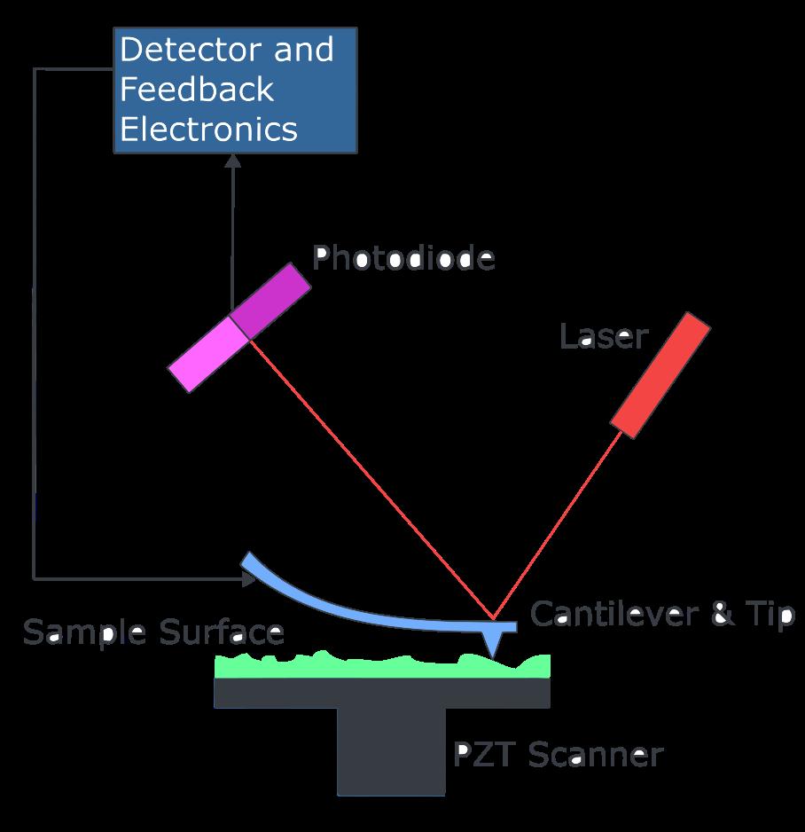
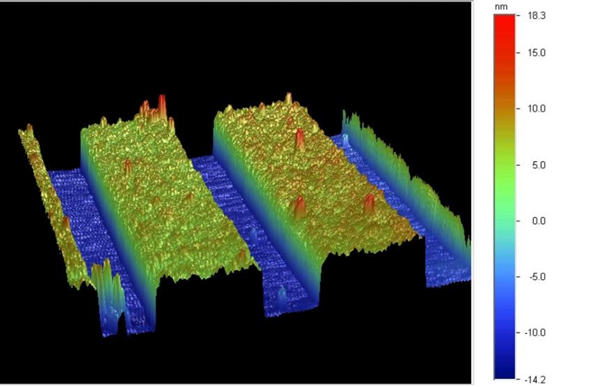
40 Atomic Force Microscopy Wikipedia Veeco
41 Substrate Bonding Silicon Direct Bonding Silicon to Silicon Silicon on Insulator (SOI) Anodic Bonding Silicon to Glass (Pyrex 7740) Intermediate Adhesive Layers Lasers

42 Anodic Bonder

43 Anodic Bonding Ziaie B. et al., Hard and soft micromachining for biomems: review of techniques and examples of applications in microfluidics and drug delivery. Advanced Drug Delivery Reviews 56(2), pp (2004).
44 Summary Important thin-films include: Thermal Silicon Oxide Silicon Dioxide (SiO2) Polysilicon Silicon Nitride (Si3N4) Phosphosilicate Glass (PSG) Metal films (e.g. tungsten and aluminum) Thin films may be produced by: Thermal oxidation Physical Vapor Deposition Chemical Vapor Deposition Epitaxial Deposition Atomic Layer Deposition (ADL)
45 Ion implantation may be used to improve electrical conductivity or to control etching characteristics. Wet bulk micromachining Isotropic and anisotropic etching 3-D structure and sacrificial layers Deep Reactive Ion Etching (DRIE) Characterization with Atomic Force Microscopy Substrate bonding Silicon direct bonding Anodic bonding
Overview. Silicon Microfabrication Part 2. Introduction to BioMEMS & Medical Microdevices
 Introduction to BioMEMS & Medical Microdevices Silicon Microfabrication Part 2 Companion lecture to the textbook: Fundamentals of BioMEMS and Medical Microdevices, by Prof., http://saliterman.umn.edu/
Micromachining vs. Soft Fabrication
 Introduction to BioMEMS & Medical Microdevices Silicon Microfabrication Part 1 Companion lecture to the textbook: Fundamentals of BioMEMS and Medical Microdevices, by Prof., http://saliterman.umn.edu/
IC/MEMS Fabrication - Outline. Fabrication
 IC/MEMS Fabrication - Outline Fabrication overview Materials Wafer fabrication The Cycle: Deposition Lithography Etching Fabrication IC Fabrication Deposition Spin Casting PVD physical vapor deposition
Chapter 2 OVERVIEW OF MEMS
 6 Chapter 2 OVERVIEW OF MEMS 2.1 MEMS and Microsystems The term MEMS is an abbreviation of microelectromechanical system. MEMS contains components ofsizes in 1 micrometer to 1 millimeter. The core element
EE 5344 Introduction to MEMS. CHAPTER 3 Conventional Si Processing
 3. Conventional licon Processing Micromachining, Microfabrication. EE 5344 Introduction to MEMS CHAPTER 3 Conventional Processing Why silicon? Abundant, cheap, easy to process. licon planar Integrated
Surface Micromachining
 Surface Micromachining Micro Actuators, Sensors, Systems Group University of Illinois at Urbana-Champaign Outline Definition of surface micromachining Most common surface micromachining materials - polysilicon
ECSE-6300 IC Fabrication Laboratory Lecture 4: Dielectrics and Poly-Si Deposition. Lecture Outline
 ECSE-6300 IC Fabrication Laboratory Lecture 4: Dielectrics and Poly-Si Deposition Prof. Rensselaer Polytechnic Institute Troy, NY 12180 Office: CII-6229 Tel.: (518) 276-2909 e-mails: luj@rpi.edu http://www.ecse.rpi.edu/courses/s18/ecse
Mostafa Soliman, Ph.D. May 5 th 2014
 Mostafa Soliman, Ph.D. May 5 th 2014 Mostafa Soliman, Ph.D. 1 Basic MEMS Processes Front-End Processes Back-End Processes 2 Mostafa Soliman, Ph.D. Wafers Deposition Lithography Etch Chips 1- Si Substrate
PHYS 534 (Fall 2008) Process Integration OUTLINE. Examples of PROCESS FLOW SEQUENCES. >Surface-Micromachined Beam
 Process Integration OUTLINE. Examples of PROCESS FLOW SEQUENCES. >Surface-Micromachined Beam") PHYS 534 (Fall 2008) Process Integration Srikar Vengallatore, McGill University 1 OUTLINE Examples of PROCESS FLOW SEQUENCES >Semiconductor diode >Surface-Micromachined Beam Critical Issues in Process
PHYS 534 (Fall 2008) Process Integration Srikar Vengallatore, McGill University 1 OUTLINE Examples of PROCESS FLOW SEQUENCES >Semiconductor diode >Surface-Micromachined Beam Critical Issues in Process
Semiconductor Manufacturing Process 10/11/2005
 Semiconductor Manufacturing Process 10/11/2005 Photolithography Oxidation CVD PVD Photolithography The purpose of photolithography is to imprint the desired pattern of a micro component on a substrate,
Chemical Vapor Deposition
 Chemical Vapor Deposition ESS4810 Lecture Fall 2010 Introduction Chemical vapor deposition (CVD) forms thin films on the surface of a substrate by thermal decomposition and/or reaction of gas compounds
Czochralski Crystal Growth
 Czochralski Crystal Growth Crystal Pulling Crystal Ingots Shaping and Polishing 300 mm wafer 1 2 Advantage of larger diameter wafers Wafer area larger Chip area larger 3 4 Large-Diameter Wafer Handling
Manufacturing Technologies for MEMS and SMART SENSORS
 4 Manufacturing Technologies for MEMS and SMART SENSORS Dr. H. K. Verma Distinguished Professor (EEE) Sharda University, Greater Noida (Formerly: Deputy Director and Professor of Instrumentation Indian
ME 189 Microsystems Design and Manufacture. Chapter 9. Micromanufacturing
 ME 189 Microsystems Design and Manufacture Chapter 9 Micromanufacturing This chapter will offer an overview of the application of the various fabrication techniques described in Chapter 8 in the manufacturing
Lecture Day 2 Deposition
 Deposition Lecture Day 2 Deposition PVD - Physical Vapor Deposition E-beam Evaporation Thermal Evaporation (wire feed vs boat) Sputtering CVD - Chemical Vapor Deposition PECVD LPCVD MVD ALD MBE Plating
Today s Class. Materials for MEMS
 Lecture 2: VLSI-based Fabrication for MEMS: Fundamentals Prasanna S. Gandhi Assistant Professor, Department of Mechanical Engineering, Indian Institute of Technology, Bombay, Recap: Last Class What is
Chapter 7 Polysilicon and Dielectric Film Deposition
 Chapter 7 Polysilicon and Dielectric Film Deposition Professor Paul K. Chu Thin Films in Microelectronics Polycrystalline silicon or polysilicon Doped or undoped silicon dioxide Stoichiometric or plasma-deposited
Atomic Layer Deposition(ALD)
") Atomic Layer Deposition(ALD) AlO x for diffusion barriers OLED displays http://en.wikipedia.org/wiki/atomic_layer_deposition#/media/file:ald_schematics.jpg Lam s market-leading ALTUS systems combine CVD
Atomic Layer Deposition(ALD) AlO x for diffusion barriers OLED displays http://en.wikipedia.org/wiki/atomic_layer_deposition#/media/file:ald_schematics.jpg Lam s market-leading ALTUS systems combine CVD
L5: Micromachining processes 1/7 01/22/02
 97.577 L5: Micromachining processes 1/7 01/22/02 5: Micromachining technology Top-down approaches to building large (relative to an atom or even a transistor) structures. 5.1 Bulk Micromachining A bulk
Lecture 8. Deposition of dielectrics and metal gate stacks (CVD, ALD)
") Lecture 8 Deposition of dielectrics and metal gate stacks (CVD, ALD) Thin Film Deposition Requirements Many films, made of many different materials are deposited during a standard CMS process. Gate Electrodes
Lecture 8 Deposition of dielectrics and metal gate stacks (CVD, ALD) Thin Film Deposition Requirements Many films, made of many different materials are deposited during a standard CMS process. Gate Electrodes
Fabrication Technology
 Fabrication Technology By B.G.Balagangadhar Department of Electronics and Communication Ghousia College of Engineering, Ramanagaram 1 OUTLINE Introduction Why Silicon The purity of Silicon Czochralski
Microstructure of Electronic Materials. Amorphous materials. Single-Crystal Material. Professor N Cheung, U.C. Berkeley
 Microstructure of Electronic Materials Amorphous materials Single-Crystal Material 1 The Si Atom The Si Crystal diamond structure High-performance semiconductor devices require defect-free crystals 2 Crystallographic
Lecture 22: Integrated circuit fabrication
 Lecture 22: Integrated circuit fabrication Contents 1 Introduction 1 2 Layering 4 3 Patterning 7 4 Doping 8 4.1 Thermal diffusion......................... 10 4.2 Ion implantation.........................
Silicon Epitaxial CVD Want to create very sharp PN boundary grow one type layer on other in single crystal form High dopant layers on low dopant
 Silicon Epitaxial CVD Want to create very sharp PN boundary grow one type layer on other in single crystal form High dopant layers on low dopant substrate Creates latch up protection for CMOS Buried Epi
MEMS Fabrication. Beyond Integrated Circuits. MEMS Basic Concepts
 MEMS Fabrication Beyond Integrated Circuits MEMS Basic Concepts Uses integrated circuit fabrication techniques to make mechanical as well as electrical components on a single chip. Small size 1µm 1mm Typically
1 MARCH 2017 FILM DEPOSITION NANOTECHNOLOGY
 1 MARCH 2017 FILM DEPOSITION NANOTECHNOLOGY PRESENTATION Pedro C. Feijoo E-mail: PedroCarlos.Feijoo@uab.cat FABRICATION TECHNOLOGIES FOR NANOELECTRONIC DEVICES. PEDRO C. FEIJOO 2 FILM GROWTH Chemical vapor
Chapter 3 Silicon Device Fabrication Technology
 Chapter 3 Silicon Device Fabrication Technology Over 10 15 transistors (or 100,000 for every person in the world) are manufactured every year. VLSI (Very Large Scale Integration) ULSI (Ultra Large Scale
Metallization deposition and etching. Material mainly taken from Campbell, UCCS
 Metallization deposition and etching Material mainly taken from Campbell, UCCS Application Metallization is back-end processing Metals used are aluminum and copper Mainly involves deposition and etching,
Activities in Plasma Process Technology at SENTECH Instruments GmbH, Berlin. Dr. Frank Schmidt
 Activities in Plasma Process Technology at SENTECH Instruments GmbH, Berlin Dr. Frank Schmidt The Company Company Private company, founded 1990 80 employees ISO 9001 Location Science & Technology Park,
Surface micromachining and Process flow part 1
 Surface micromachining and Process flow part 1 Identify the basic steps of a generic surface micromachining process Identify the critical requirements needed to create a MEMS using surface micromachining
Semiconductor Technology
 Semiconductor Technology from A to Z Oxidation www.halbleiter.org Contents Contents List of Figures List of Tables II III 1 Oxidation 1 1.1 Overview..................................... 1 1.1.1 Application...............................
Lect. 2: Basics of Si Technology
 Unit processes Thin Film Deposition Etching Ion Implantation Photolithography Chemical Mechanical Polishing 1. Thin Film Deposition Layer of materials ranging from fractions of nanometer to several micro-meters
CSI G SYSTEMS CSI GAS DELIVERY SUPPORT. Chemical Vapor Deposition (CVD)
") This page discusses the CVD processes often used for integrated circuits (ICs). Particular materials are deposited best under particular conditions. Facilitation recommendations are at the bottom of the
This page discusses the CVD processes often used for integrated circuits (ICs). Particular materials are deposited best under particular conditions. Facilitation recommendations are at the bottom of the
Surface Micromachining
 Surface Micromachining Outline Introduction Material often used in surface micromachining Material selection criteria in surface micromachining Case study: Fabrication of electrostatic motor Major issues
Ion Implantation Most modern devices doped using ion implanters Ionize gas sources (single +, 2+ or 3+ ionization) Accelerate dopant ions to very
 Accelerate dopant ions to very") Ion Implantation Most modern devices doped using ion implanters Ionize gas sources (single +, 2+ or 3+ ionization) Accelerate dopant ions to very high voltages (10-600 KeV) Use analyzer to selection charge/mass
Ion Implantation Most modern devices doped using ion implanters Ionize gas sources (single +, 2+ or 3+ ionization) Accelerate dopant ions to very high voltages (10-600 KeV) Use analyzer to selection charge/mass
Fabrication Process. Crystal Growth Doping Deposition Patterning Lithography Oxidation Ion Implementation CONCORDIA VLSI DESIGN LAB
 Fabrication Process Crystal Growth Doping Deposition Patterning Lithography Oxidation Ion Implementation 1 Fabrication- CMOS Process Starting Material Preparation 1. Produce Metallurgical Grade Silicon
Microelettronica. Planar Technology for Silicon Integrated Circuits Fabrication. 26/02/2017 A. Neviani - Microelettronica
 Microelettronica Planar Technology for Silicon Integrated Circuits Fabrication 26/02/2017 A. Neviani - Microelettronica Introduction Simplified crosssection of an nmosfet and a pmosfet Simplified crosssection
Etching Etching Definitions Isotropic Etching: same in all direction Anisotropic Etching: direction sensitive Selectivity: etch rate difference
 Etching Etching Definitions Isotropic Etching: same in all direction Anisotropic Etching: direction sensitive Selectivity: etch rate difference between 2 materials Need strong selectivity from masking
EECS130 Integrated Circuit Devices
 EECS130 Integrated Circuit Devices Professor Ali Javey 9/13/2007 Fabrication Technology Lecture 1 Silicon Device Fabrication Technology Over 10 15 transistors (or 100,000 for every person in the world)
INF5490 RF MEMS. LN02: MEMS Fabrication. Spring 2012, Oddvar Søråsen Department of Informatics, UoO
 INF5490 RF MEMS LN02: MEMS Fabrication Spring 2012, Oddvar Søråsen Department of Informatics, UoO 1 Micromachining Today s lecture Important process steps General Summary: MEMS-specific steps Examples
National Nano Fabrication Centre (NNFC)
") National Nano Fabrication Centre (NNFC) Tool and Process Capabilities 1. Lithography 1.1 Direct Laser Writer/Lithography 1.1.1 Preferred Design file format: GDS2 or CIF 1.1.2 Please note that coloured
National Nano Fabrication Centre (NNFC) Tool and Process Capabilities 1. Lithography 1.1 Direct Laser Writer/Lithography 1.1.1 Preferred Design file format: GDS2 or CIF 1.1.2 Please note that coloured
Chapter 4. UEEP2613 Microelectronic Fabrication. Oxidation
 Chapter 4 UEEP2613 Microelectronic Fabrication Oxidation Prepared by Dr. Lim Soo King 24 Jun 2012 Chapter 4...113 Oxidation...113 4.0 Introduction... 113 4.1 Chemistry of Silicon Dioxide Formation... 115
EE 330 Lecture 8. IC Fabrication Technology Part II. - Oxidation - Epitaxy - Polysilicon - Interconnects
 EE 330 Lecture 8 IC Fabrication Technology Part II - Oxidation - Epitaxy - Polysilicon - Interconnects Review from Last Time MOS Transistor Bulk Source Gate Drain p-channel MOSFET Lightly-doped n-type
Chapter 2 MOS Fabrication Technology
 Chapter 2 MOS Fabrication Technology Abstract This chapter is concerned with the fabrication of metal oxide semiconductor (MOS) technology. Various processes such as wafer fabrication, oxidation, mask
Doping and Oxidation
 Technische Universität Graz Institute of Solid State Physics Doping and Oxidation Franssila: Chapters 13,14, 15 Peter Hadley Technische Universität Graz Institute of Solid State Physics Doping Add donors
INTEGRATED-CIRCUIT TECHNOLOGY
 INTEGRATED-CIRCUIT TECHNOLOGY 0. Silicon crystal growth and wafer preparation 1. Processing Steps 1.1. Photolitography 1.2. Oxidation 1.3. Layer Deposition 1.4. Etching 1.5. Diffusion 1.6 Backend: assembly,
Review of CMOS Processing Technology
 - Scaling and Integration Moore s Law Unit processes Thin Film Deposition Etching Ion Implantation Photolithography Chemical Mechanical Polishing 1. Thin Film Deposition Layer of materials ranging from
Silicon Manufacturing
 Silicon Manufacturing Group Members Young Soon Song Nghia Nguyen Kei Wong Eyad Fanous Hanna Kim Steven Hsu th Fundamental Processing Steps 1.Silicon Manufacturing a) Czochralski method. b) Wafer Manufacturing
Change in stoichiometry
 Measurement of Gas Sensor Performance Gas sensing materials: 1. Sputtered ZnO film (150 nm (Massachusetts Institute of Technology) 2. Sputtered SnO 2 film (60 nm) (Fraunhofer Institute of Physical Measurement
ME 141B: The MEMS Class Introduction to MEMS and MEMS Design. Sumita Pennathur UCSB
 ME 141B: The MEMS Class Introduction to MEMS and MEMS Design Sumita Pennathur UCSB Outline today Introduction to thin films Oxidation Deal-grove model CVD Epitaxy Electrodeposition 10/6/10 2/45 Creating
A discussion of crystal growth, lithography, etching, doping, and device structures is presented in
 Chapter 5 PROCESSING OF DEVICES A discussion of crystal growth, lithography, etching, doping, and device structures is presented in the following overview gures. SEMICONDUCTOR DEVICE PROCESSING: AN OVERVIEW
Lecture 10: MultiUser MEMS Process (MUMPS)
") MEMS: Fabrication Lecture 10: MultiUser MEMS Process (MUMPS) Prasanna S. Gandhi Assistant Professor, Department of Mechanical Engineering, Indian Institute of Technology, Bombay, 1 Recap Various VLSI based
MEMS: Fabrication Lecture 10: MultiUser MEMS Process (MUMPS) Prasanna S. Gandhi Assistant Professor, Department of Mechanical Engineering, Indian Institute of Technology, Bombay, 1 Recap Various VLSI based
2. Fabrication techniques. KNU Seminar Course 2015 Robert Mroczyński
 2. Fabrication techniques KNU Seminar Course 2015 Robert Mroczyński Technological layers used in the course of the IC fabrication Semiconductors Fundamental part of each IC, active material of semiconductor
Physical Vapor Deposition (PVD) Zheng Yang
 Zheng Yang") Physical Vapor Deposition (PVD) Zheng Yang ERF 3017, email: yangzhen@uic.edu Page 1 Major Fabrication Steps in MOS Process Flow UV light Mask oxygen Silicon dioxide photoresist exposed photoresist oxide
Physical Vapor Deposition (PVD) Zheng Yang ERF 3017, email: yangzhen@uic.edu Page 1 Major Fabrication Steps in MOS Process Flow UV light Mask oxygen Silicon dioxide photoresist exposed photoresist oxide
Gaetano L Episcopo. Introduction to MEMS
 Gaetano L Episcopo Introduction to MEMS What are MEMS? Micro Electro Mechanichal Systems MEMS are integrated devices, or systems of devices, with microscopic parts, such as: Mechanical Parts Electrical
Wafer (1A) Young Won Lim 4/30/13
 Young Won Lim 4/30/13") Copyright (c) 2011-2013 Young W. Lim. Permission is granted to copy, distribute and/or modify this document under the terms of the GNU Free Documentation License, Version 1.2 or any later version published
Copyright (c) 2011-2013 Young W. Lim. Permission is granted to copy, distribute and/or modify this document under the terms of the GNU Free Documentation License, Version 1.2 or any later version published
Lecture 8 Chemical Vapor Deposition (CVD)
") Lecture 8 Chemical Vapor Deposition (CVD) Chapter 5 & 6 Wolf and Tauber 1/88 Announcements Homework: Homework Number 2 is due on Thursday (19 th October). Homework will be returned one week later Thursday
Lecture 8 Chemical Vapor Deposition (CVD) Chapter 5 & 6 Wolf and Tauber 1/88 Announcements Homework: Homework Number 2 is due on Thursday (19 th October). Homework will be returned one week later Thursday
Micromachining AMT 2505
 Micromachining AMT 2505 Shanmuga Raja.B (BVB0912004) Module leader : Mr. Raja Hussain Introduction Micromachining are inherently connected to the evolution of Micro Electro Mechanical Systems (MEMS). Decades
Introduction to CMOS VLSI Design. Layout, Fabrication, and Elementary Logic Design
 Introduction to CMOS VLSI Design Layout, Fabrication, and Elementary Logic Design CMOS Fabrication CMOS transistors are fabricated on silicon wafer Lithography process similar to printing press On each
Solid State Sensors. Microfabrication 8/22/08 and 8/25/08
 Solid State Sensors Microfabrication 8/22/08 and 8/25/08 Purpose of This Material To introduce the student to microfabrication techniques as used to fabricate MEMS Sensors Understand concepts not specifics
SURFACE MICROMACHINING
 SURFACE MICROMACHINING Features are built up, layer by layer on the surface of a substrate. Surface micromachined devices are much smaller than bulk micromachined components. Nature of deposition process
The Physical Structure (NMOS)
") The Physical Structure (NMOS) Al SiO2 Field Oxide Gate oxide S n+ Polysilicon Gate Al SiO2 SiO2 D n+ L channel P Substrate Field Oxide contact Metal (S) n+ (G) L W n+ (D) Poly 1 3D Perspective 2 3 Fabrication
The Physical Structure (NMOS) Al SiO2 Field Oxide Gate oxide S n+ Polysilicon Gate Al SiO2 SiO2 D n+ L channel P Substrate Field Oxide contact Metal (S) n+ (G) L W n+ (D) Poly 1 3D Perspective 2 3 Fabrication
Nanoelectronics Fabrication Facility
 Nanoelectronics Fabrication Facility Contents Introduction 2 Mask Making Module 4 Photolithography Module 6 Wet Etching and CMP Module 8 Dry Etching and Sputtering Module 10 Thermal Process and Implantation
6.777J/2.732J Design and Fabrication of Microelectromechanical Devices Spring Term Solution to Problem Set 2 (16 pts)
") 6.777J/2.732J Design and Fabrication of Microelectromechanical Devices Spring Term 2007 By Brian Taff (Adapted from work by Feras Eid) Solution to Problem Set 2 (16 pts) Issued: Lecture 4 Due: Lecture
6.777J/2.732J Design and Fabrication of Microelectromechanical Devices Spring Term 2007 By Brian Taff (Adapted from work by Feras Eid) Solution to Problem Set 2 (16 pts) Issued: Lecture 4 Due: Lecture
EE 330 Lecture 9. IC Fabrication Technology Part 2
 EE 330 Lecture 9 IC Fabrication Technology Part 2 Quiz 8 A 2m silicon crystal is cut into wafers using a wire saw. If the wire diameter is 220um and the wafer thickness is 350um, how many wafers will this
Institute of Solid State Physics. Technische Universität Graz. Deposition. Franssila: Chapters 5 & 6. Peter Hadley
 Technische Universität Graz Institute of Solid State Physics Deposition Franssila: Chapters 5 & 6 Peter Hadley Silicon wafers Total Thickness Variation: a good 8" Prime wafer would be < 15 m Site flatness
ELEC 3908, Physical Electronics, Lecture 4. Basic Integrated Circuit Processing
 ELEC 3908, Physical Electronics, Lecture 4 Basic Integrated Circuit Processing Lecture Outline Details of the physical structure of devices will be very important in developing models for electrical behavior
General Introduction to Microstructure Technology p. 1 What is Microstructure Technology? p. 1 From Microstructure Technology to Microsystems
 General Introduction to Microstructure Technology p. 1 What is Microstructure Technology? p. 1 From Microstructure Technology to Microsystems Technology p. 9 The Parallels to Microelectronics p. 15 The
Chapter 5 Thermal Processes
 Chapter 5 Thermal Processes 1 Topics Introduction Hardware Oxidation Diffusion Annealing Post-Implantation Alloying Reflow High Temp CVD Epi Poly Silicon Nitride RTP RTA RTP Future Trends 2 Definition
Microstructures using RF sputtered PSG film as a sacrificial layer in surface micromachining
 Sādhanā Vol. 34, Part 4, August 2009, pp. 557 562. Printed in India Microstructures using RF sputtered PSG film as a sacrificial layer in surface micromachining VIVEKANAND BHATT 1,, SUDHIR CHANDRA 1 and
Fabrication Technology, Part II
 EEL5225: Principles of MEMS Transducers (Fall 2003) Fabrication Technology, Part II Agenda: Process Examples TI Micromirror fabrication process SCREAM CMOS-MEMS processes Wafer Bonding LIGA Reading: Senturia,
Mikrosensorer. Microfabrication 1
 Mikrosensorer Microfabrication 1 Literature Introductory MEMS Fabrication and Applications Thomas M. Adams and Richard A. Layton Available as ebook on http://www.lub.lu.se/en/search/lubsearch.html This
Semiconductor Technology
 Semiconductor Technology von A bis Z Metallization www.halbleiter.org Contents Contents List of Figures List of Tables II III 1 Metallization 1 1.1 Requirements on metallization........................
Most semiconductor devices contain at least one junction between p-type and n-type material. These p-n junctions are fundamental to the performance
 Ch. 5: p-n Junction Most semiconductor devices contain at least one junction between p-type and n-type material. These p-n junctions are fundamental to the performance of functions such as rectification,
Semiconductor Device Fabrication
 5 May 2003 Review Homework 6 Semiconductor Device Fabrication William Shockley, 1945 The network before the internet Bell Labs established a group to develop a semiconductor replacement for the vacuum
Ion Implantation Most modern devices doped using ion implanters Implant dopants by accelerating individual atoms (ions) Ionize gas sources (single +,
 Ionize gas sources (single +,") Ion Implantation Most modern devices doped using ion implanters Implant dopants by accelerating individual atoms (ions) Ionize gas sources (single +, 2+ or 3+ ionization) Use analyzer to selection charge/mass
Ion Implantation Most modern devices doped using ion implanters Implant dopants by accelerating individual atoms (ions) Ionize gas sources (single +, 2+ or 3+ ionization) Use analyzer to selection charge/mass
3. Overview of Microfabrication Techniques
 3. Overview of Microfabrication Techniques The Si revolution First Transistor Bell Labs (1947) Si integrated circuits Texas Instruments (~1960) Modern ICs More? Check out: http://www.pbs.org/transistor/background1/events/miraclemo.html
3. Photolithography, patterning and doping techniques. KNU Seminar Course 2015 Robert Mroczyński
 3. Photolithography, patterning and doping techniques KNU Seminar Course 2015 Robert Mroczyński Critical technology processes Photolithography The aim of this process is to transfer (in the most accurate
Fabrication Technology, Part I
 EEL5225: Principles of MEMS Transducers (Fall 2003) Fabrication Technology, Part I Agenda: Oxidation, layer deposition (last lecture) Lithography Pattern Transfer (etching) Impurity Doping Reading: Senturia,
VLSI INTRODUCTION P.VIDYA SAGAR ( ASSOCIATE PROFESSOR) Department of Electronics and Communication Engineering, VBIT
 Department of Electronics and Communication Engineering, VBIT") VLSI INTRODUCTION P.VIDYA SAGAR ( ASSOCIATE PROFESSOR) contents UNIT I INTRODUCTION: Introduction to IC Technology MOS, PMOS, NMOS, CMOS & BiCMOS technologies. BASIC ELECTRICAL PROPERTIES : Basic Electrical
VLSI INTRODUCTION P.VIDYA SAGAR ( ASSOCIATE PROFESSOR) contents UNIT I INTRODUCTION: Introduction to IC Technology MOS, PMOS, NMOS, CMOS & BiCMOS technologies. BASIC ELECTRICAL PROPERTIES : Basic Electrical
Chapter 3 CMOS processing technology
 Chapter 3 CMOS processing technology (How to make a CMOS?) Si + impurity acceptors(p-type) donors (n-type) p-type + n-type => pn junction (I-V) 3.1.1 (Wafer) Wafer = A disk of silicon (0.25 mm - 1 mm thick),
About Cambridge NanoTech Atomic Layer Deposition (ALD) Selected Applications Manufacturing Considerations ALD Reactors Summary
 Selected Applications Manufacturing Considerations ALD Reactors Summary") About Cambridge NanoTech Atomic Layer Deposition (ALD) Selected Applications Manufacturing Considerations ALD Reactors Summary Founded in 2003 by Dr. Jill Becker Located in Cambridge, MA Grew directly
About Cambridge NanoTech Atomic Layer Deposition (ALD) Selected Applications Manufacturing Considerations ALD Reactors Summary Founded in 2003 by Dr. Jill Becker Located in Cambridge, MA Grew directly
Lecture #18 Fabrication OUTLINE
 Transistors on a Chip Lecture #18 Fabrication OUTLINE IC Fabrication Technology Introduction the task at hand Doping Oxidation Thin-film deposition Lithography Etch Lithography trends Plasma processing
Additive Techniques. Thermal Oxidation of silicon
 Additive Techniques Elements required in MEMS/ IC context Si, Al, Au, Ti, W, Cu, Cr, O, N, Ni-Fe alloys}-mems and IC S. Zr, Ta, Ir, C, Pt, Pd, Ag, Zn, and Nb}- MEMS only. In sensors and biomedical devices
CMOS Fabrication. Dr. Bassam Jamil. Adopted from slides of the textbook
 CMOS Fabrication Dr. Bassam Jamil Adopted from slides of the textbook CMOS Fabrication CMOS transistors are fabricated on silicon wafer Lithography process similar to printing press On each step, different
PlasmaPro TM System100 & System133. Modular tools for wafer processing100
 TM System100 & System133 Modular tools for wafer processing100 System100 & System133 Plasma etch & deposition process modules Oxford Instruments System100 and System133 process modules are built on 200mm
Oxidation SMT Yau - 1
 Oxidation Yau - 1 Objectives After studying the material in this chapter, you will be able to: 1. Describe an oxide film for semiconductor manufacturing, including its atomic structure, how it is used
Microelectronics. Integrated circuits. Introduction to the IC technology M.Rencz 11 September, Expected decrease in line width
 Microelectronics Introduction to the IC technology M.Rencz 11 September, 2002 9/16/02 1/37 Integrated circuits Development is controlled by the roadmaps. Self-fulfilling predictions for the tendencies
Thermal Evaporation. Theory
 Thermal Evaporation Theory 1. Introduction Procedures for depositing films are a very important set of processes since all of the layers above the surface of the wafer must be deposited. We can classify
EE C245 ME C218 Introduction to MEMS Design Fall 2011
 Lecture Outline EE C245 ME C218 Introduction to MEMS Design Fall 2011 Prof. Clark T.-C. Nguyen Dept. of Electrical Engineering & Computer Sciences University of California at Berkeley Berkeley, CA 94720
HOMEWORK 4 and 5. March 15, Homework is due on Monday March 30, 2009 in Class. Answer the following questions from the Course Textbook:
 HOMEWORK 4 and 5 March 15, 2009 Homework is due on Monday March 30, 2009 in Class. Chapter 7 Answer the following questions from the Course Textbook: 7.2, 7.3, 7.4, 7.5, 7.6*, 7.7, 7.9*, 7.10*, 7.16, 7.17*,
Device Fabrication: CVD and Dielectric Thin Film
 Device Fabrication: CVD and Dielectric Thin Film 1 Objectives Identify at least four CVD applications Describe CVD process sequence List the two deposition regimes and describe their relation to temperature
Fabrication and Layout
 ECEN454 Digital Integrated Circuit Design Fabrication and Layout ECEN 454 3.1 A Glimpse at MOS Device Polysilicon Aluminum ECEN 475 4.2 1 Material Classification Insulators Glass, diamond, silicon oxide
Instructor: Dr. M. Razaghi. Silicon Oxidation
 SILICON OXIDATION Silicon Oxidation Many different kinds of thin films are used to fabricate discrete devices and integrated circuits. Including: Thermal oxides Dielectric layers Polycrystalline silicon
There are basically two approaches for bulk micromachining of. silicon, wet and dry. Wet bulk micromachining is usually carried out
 57 Chapter 3 Fabrication of Accelerometer 3.1 Introduction There are basically two approaches for bulk micromachining of silicon, wet and dry. Wet bulk micromachining is usually carried out using anisotropic
EE40 Lec 22. IC Fabrication Technology. Prof. Nathan Cheung 11/19/2009
 Suggested Reading EE40 Lec 22 IC Fabrication Technology Prof. Nathan Cheung 11/19/2009 300mm Fab Tour http://www-03.ibm.com/technology/manufacturing/technology_tour_300mm_foundry.html Overview of IC Technology
Process Flow in Cross Sections
 Process Flow in Cross Sections Process (simplified) 0. Clean wafer in nasty acids (HF, HNO 3, H 2 SO 4,...) --> wear gloves! 1. Grow 500 nm of SiO 2 (by putting the wafer in a furnace with O 2 2. Coat