Aligned Carbon Nanofibre-Polymer Composite Membranes. CNT Growth and Manipulation. Eleanor Campbell Dept. of Physics, Göteborg University
|
|
|
- Willa Lane
- 6 years ago
- Views:
Transcription


1 Aligned Carbon Nanofibre-Polymer Composite Membranes CNT Growth and Manipulation Eleanor Campbell Dept. of Physics, Göteborg University
2 Plasma CVD Growth Polymer/Nanofibre Composite Low ambient temperature growth Dielectrophoretic separation of metallic and semiconducting SWNT & its use in device fabrication (if time)


3 Plasma CVD Growth of Nanotubes /fibres T = 700 C Ni catalyst C 2 H 2 :NH 3 = 1:5, 4 Torr tip-grown fibres Fe catalyst C 2 H 2 :H 2 = 1:3 7 Torr base-grown MWNT Ni Fe


")
4 Growth Quality depends critically on Plasma Current Density 1.5 ma/cm 2 Array growth on Mo substrate C 2 H 2 :NH 3 = 1:5 Kabir et al., Nanotech. 16 (2005) 458 Kabir et al., Nanotech. 17 (2006) ma/cm 2
5 M. Jönsson Optical spectroscopy shows the relative decrease in molecular/atomic precursors and also a clear increase in CN intensity beyond 30 ma (4.5 ma/cm 2 ) - Onset of non-catalytic deposition and increased sputtering
 ma/cm 2 1 (d) 10 ma/cm 2 0 0 20 40 60 80 100 120 140 160 180 200 220 240 260 280 300 Time (min) Can these vertically aligned CNF be used")
6 B. Gindre ma/cm(b) 2 Length of CNFs (um) ma/cm 2 (c) 1.5 (a) ma/cm 2 1 (d) 10 ma/cm Time (min) Can these vertically aligned CNF be used to make an anistropically conducting polymer membrane? Diameter ca. 50 nm


7 Polymer CNT Composite Materials Array of individual nanotubes grown on a Mo substrate Arrays after spin-coating showing photonic-crystal effects Morjan, Gromov, Gindre


8 Electrical Characterisation Two probe measurements (-5;+5)V Deposition of gold electrodes by metal evaporation with a mask (0.5mm in diameter and 2mm apart) Mo &Mo layer Au PS+VACNF Substrate Au PS &Mo layer PS Au Substrate Au PS+VACNF & Mo layer Au PS+VACNF Substrate Au PS+VACNF & PS+VACNF layer Au PS+VACNF Substrate Au
9 Measured resistance through film without fibre i.e. Polystyrene alone (3 µm thick): 10 4 Ω With CNF: 50 Ω There are approximately nanofibres contacted for each measurement -The average resistance per fibre is ca kω (compares with ca. 100 kω for individual fibres with 0.5 ma current carrying capacity)
 Ag PS+VACNFs Ag")
10 Removing the polymer from the substrate alkali base alkali base Leave for a couple of days Few GΩ along the membrane (2mm distance) Ag PS+VACNFs Ag
 to grow. Mo Electrodes with narrow resistive bridge.")
11 How to reduce the chip temperature to make good quality CNT at temperatures lower than 450 o C (CMOS compatibility)? Use very local resistive heating only where you want the nanotube(s) to grow. Mo Electrodes with narrow resistive bridge. Catalyst deposited on bridge (5nm Al 2 O 3, 1 nm Fe) 14 ma, 2V for heating Dittmer et al., Appl. Phys. A in press

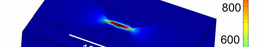

12 Temperature simulation corresponding to conditions in the experiment


 C 2 H 2 :H 2 :Ar = 10 sccm: 300")
13 Dittmer et al., Appl. Phys. A, in press Room Temperature Growth: MWNT Atmospheric pressure 7 Torr With aligning electric field No electric field applied during growth MWNT (Fe catalyst, acetylene precursor) C 2 H 2 :H 2 :Ar = 10 sccm: 300 sccm: 500 sccm


14 nm diameter Raman AFM Replace acetylene with ethylene SWNT Chip at 60 o C

15 Growth stops when temperature falls below ca. 500 o C
16 Thanks to: Array Growth and Membranes: Oleg Nerushev Raluca Morjan Martin Jönsson Baptiste Gindre Andrei Gromov Shafiq Kabir Nanorelay: SangWook Lee Anders Eriksson Jari Kinaret et al (theory) Dielectrophoretic Separation: Andrei Gromov Low Temperature Growth: Staffan Dittmer Oleg Nerushev

 In this way metallic nanotubes can be preferentially attracted to electrodes leaving")
17 AC Dielectrophoresis for separating metallic and semiconducting nanotubes r ε ε r 2 F ε E Re( ) ε2 + 2ε1 2: nanotube 1: solvent For semiconducting SWNT F is negative, for metallic SWNT the force is positive, attracting the CNT to the electrodes. (Krupke et al) In this way metallic nanotubes can be preferentially attracted to electrodes leaving proportionately more semiconducting SWNT in dispersion. D.S. Lee, et al., Appl. Phys. A 80 (2005), 5
18 Nanotubes left in dispersion after deposition cycles Proportion of CNTs (%) ref. Semiconducting Metallic final (7) Raman analysis Number of Deposition Cycles D.S. Lee, et al., Appl. Phys. A 80 (2005), 5
19 Laminar flow no mixing of liquids Electrodes Although the interaction time is very short we get a significant increase in metallic content of lower channel on a single pass
20 reference sample suspension in Na-DOC, λ ex. 785nm > 50% metallic metallic fraction 6mg/L in 1% Na-DOC Raman intensity, a.u m s m s wavenumbers, cm Still problem with bundle formation

, Appl. Phys. Lett. 82, 1287 (2003) L.M. Jonsson et al., J. Appl. Phys. 96, 629 (2004)")
21 Carbon Nanotube Nanorelay Carbon nanotube Source electrode Drain electrode Gate electrode high Q oscillator, logical switch, bistable memory element, Mechanical resonance frequency in GHz range, switching speed could be faster. J. Kinaret et al. (S. Viefers), Appl. Phys. Lett. 82, 1287 (2003) L.M. Jonsson et al., J. Appl. Phys. 96, 629 (2004)
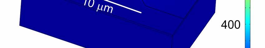
22 Nanorelay Fabrication (a) S SiO2 G D (e) (b) PMMA (d) (c) 10μm AC Acid free method to make suspended structure: S. W. Lee et. al Appl. Phys. A 78, 283 (2004)

 Axelsson et al.")
23 S.W: Lee et al., Nano Lett. 4 (2004) Introduction of critical point drying led to 75% suspension length (nm) thickness (nm) Axelsson et al., New J. Phys 7 (2005) 245
24 I source-drain vs Gate Voltage, V SD = 0.5 V Current (μa) Current (μa) Voltage (V) Voltage (V) Current (μa) Current(μA) to (1) Voltage (V) V gate (V)
Vertically aligned Ni magnetic nanowires fabricated by diblock-copolymer-directed Al thin film anodization
 Vertically aligned Ni magnetic nanowires fabricated by diblock-copolymer-directed Al thin film anodization Researcher: Kunbae (Kevin) Noh, Graduate Student, MAE Dept. and CMRR Collaborators: Leon Chen,
ENS 06 Paris, France, December 2006
 CARBON NANOTUBE ARRAY VIAS FOR INTERCONNECT APPLICATIONS Jyh-Hua ng 1, Ching-Chieh Chiu 2, Fuang-Yuan Huang 2 1 National Nano Device Laboratories, No.26, Prosperity Road I, Science-Based Industrial Park,
Visit
 Practical Applications for Nano- Electronics by Vimal Gopee E-mail: Vimal.gopee@npl.co.uk 10/10/12 Your Delegate Webinar Control Panel Open and close your panel Full screen view Raise hand for Q&A at the
Process steps for Field Emitter devices built on Silicon wafers And 3D Photovoltaics on Silicon wafers
 Process steps for Field Emitter devices built on Silicon wafers And 3D Photovoltaics on Silicon wafers David W. Stollberg, Ph.D., P.E. Research Engineer and Adjunct Faculty GTRI_B-1 Field Emitters GTRI_B-2
Journal of Chemical and Pharmaceutical Research, 2017, 9(1): Research Article
: Research Article") Available online www.jocpr.com Journal of Chemical and Pharmaceutical Research, 2017, 9(1):163-167 Research Article ISSN : 0975-7384 CODEN(USA) : JCPRC5 Synthesis and Characterization of Carbon Nano Spheres
Available online www.jocpr.com Journal of Chemical and Pharmaceutical Research, 2017, 9(1):163-167 Research Article ISSN : 0975-7384 CODEN(USA) : JCPRC5 Synthesis and Characterization of Carbon Nano Spheres
CREOL, The College of Optics & Photonics, University of Central Florida
 Metal Substrate Induced Control of Ag Nanoparticle Plasmon Resonances for Tunable SERS Substrates Pieter G. Kik 1, Amitabh Ghoshal 1, Manuel Marquez 2 and Min Hu 1 1 CREOL, The College of Optics and Photonics,
350 C for 8 hours in argon atmosphere. Supplementary Figures. Supplementary Figure 1 High-temperature annealing of BP flakes on SiO 2.
 Supplementary Figures Supplementary Figure 1 High-temperature annealing of BP flakes on SiO 2. (a-d) The optical images of three BP flakes on a SiO 2 substrate before (a,b) and after annealing (c,d) at
Boron doped diamond deposited by microwave plasma-assisted CVD at low and high pressures
 Available online at www.sciencedirect.com Diamond & Related Materials 17 (2008) 481 485 www.elsevier.com/locate/diamond Boron doped diamond deposited by microwave plasma-assisted CVD at low and high pressures
Oligomer-Coated Carbon Nanotube Chemiresistive Sensors for Selective Detection of Nitroaromatic Explosives
 Supporting information for Oligomer-Coated Carbon Nanotube Chemiresistive Sensors for Selective Detection of Nitroaromatic Explosives Yaqiong Zhang, Miao Xu, Benjamin R. Bunes, Na Wu, Dustin E. Gross,,
Surface Preparation and Cleaning Conference April 19-20, 2016, Santa Clara, CA, USA. Nano-Bio Electronic Materials and Processing Lab.
 Surface Preparation and Cleaning Conference April 19-20, 2016, Santa Clara, CA, USA Issues on contaminants on EUV mask Particle removal on EUV mask surface Carbon contamination removal on EUV mask surface
Multiphoton lithography based 3D micro/nano printing Dr Qin Hu
 Multiphoton lithography based 3D micro/nano printing Dr Qin Hu EPSRC Centre for Innovative Manufacturing in Additive Manufacturing University of Nottingham Multiphoton lithography Also known as direct
Metallization deposition and etching. Material mainly taken from Campbell, UCCS
 Metallization deposition and etching Material mainly taken from Campbell, UCCS Application Metallization is back-end processing Metals used are aluminum and copper Mainly involves deposition and etching,
Morphology of Thin Aluminum Film Grown by DC Magnetron Sputtering onto SiO 2 on Si(100) Substrate
 Substrate") Morphology of Thin Aluminum Film Grown by DC Magnetron Sputtering onto SiO 2 on Si(1) Substrate Fan Wu Microelectronics Center, Medtronic Inc., Tempe, AZ 85261 James E. Morris Department of Electrical
Morphology of Thin Aluminum Film Grown by DC Magnetron Sputtering onto SiO 2 on Si(1) Substrate Fan Wu Microelectronics Center, Medtronic Inc., Tempe, AZ 85261 James E. Morris Department of Electrical
Growth and Doping of SiC-Thin Films on Low-Stress, Amorphous Si 3 N 4 /Si Substrates for Robust Microelectromechanical Systems Applications
 Journal of ELECTRONIC MATERIALS, Vol. 31, No. 5, 2002 Special Issue Paper Growth and Doping of SiC-Thin Films on Low-Stress, Amorphous Si 3 N 4 /Si Substrates for Robust Microelectromechanical Systems
Toward Controllable Growth of Carbon Nanotubes
 Honda Research Institute USA Inc. Toward Controllable Growth of Carbon Nanotubes Avetik R. Harutyunyan Materials Science Division, Columbus Ohio, USA (April 10, 2011) The 5 th Rice University/Air Force
MEMS prototyping using RF sputtered films
 Indian Journal of Pure & Applied Physics Vol. 45, April 2007, pp. 326-331 MEMS prototyping using RF sputtered films Sudhir Chandra, Vivekanand Bhatt, Ravindra Singh, Preeti Sharma & Prem Pal* Centre for
TSV Processing and Wafer Stacking. Kathy Cook and Maggie Zoberbier, 3D Business Development
 TSV Processing and Wafer Stacking Kathy Cook and Maggie Zoberbier, 3D Business Development Outline Why 3D Integration? TSV Process Variations Lithography Process Results Stacking Technology Wafer Bonding
EE40 Lec 22. IC Fabrication Technology. Prof. Nathan Cheung 11/19/2009
 Suggested Reading EE40 Lec 22 IC Fabrication Technology Prof. Nathan Cheung 11/19/2009 300mm Fab Tour http://www-03.ibm.com/technology/manufacturing/technology_tour_300mm_foundry.html Overview of IC Technology
Free standing Multilayer Thin Film of Cellulose Nanocrystals
 Free standing Multilayer Thin Film of Cellulose Nanocrystals Chaoyang Jiang Department of Chemistry The University of South Dakota Edmonton, June 25, 2009 Cellulose Nanocrystals Nanotechnology R&D Priority
EEC 118 Lecture #5: MOS Fabrication. Rajeevan Amirtharajah University of California, Davis Jeff Parkhurst Intel Corporation
 EEC 118 Lecture #5: MOS Fabrication Rajeevan Amirtharajah University of California, Davis Jeff Parkhurst Intel Corporation Announcements Lab 3 this week, report due next week HW 3 due this Friday at 4
Electron field emission from transparent multiwalled carbon nanotube sheets for inverted field emission displays
 CARBON 48 (2010) 41 46 available at www.sciencedirect.com journal homepage: www.elsevier.com/locate/carbon Electron field emission from transparent multiwalled carbon nanotube sheets for inverted field
Supplementary Figure S1 Crystal structure of the conducting filaments in sputtered SiO 2
 Supplementary Figure S1 Crystal structure of the conducting filaments in sputtered SiO 2 based devices. (a) TEM image of the conducting filament in a SiO 2 based memory device used for SAED analysis. (b)
Solar Cells and Photosensors.
 Designing Photonic Crystals in Strongly Absorbing Material for Applications in Solar Cells and Photosensors. Minda Wagenmaker 1, Ebuka S. Arinze 2, Botong Qiu 2, Susanna M. Thon 2 1 Mechanical Engineering
HOMEWORK 4 and 5. March 15, Homework is due on Monday March 30, 2009 in Class. Answer the following questions from the Course Textbook:
 HOMEWORK 4 and 5 March 15, 2009 Homework is due on Monday March 30, 2009 in Class. Chapter 7 Answer the following questions from the Course Textbook: 7.2, 7.3, 7.4, 7.5, 7.6*, 7.7, 7.9*, 7.10*, 7.16, 7.17*,
Efficient organic distributed feedback lasers with active films imprinted by thermal nanoimprint lithography
 Efficient organic distributed feedback lasers with active films imprinted by thermal nanoimprint lithography bidali zenuenean, ondo dago. Efficient organic distributed feedback lasers with active films
Lecture 5. SOI Micromachining. SOI MUMPs. SOI Micromachining. Silicon-on-Insulator Microstructures. Agenda:
 EEL6935 Advanced MEMS (Spring 2005) Instructor: Dr. Huikai Xie SOI Micromachining Agenda: SOI Micromachining SOI MUMPs Multi-level structures Lecture 5 Silicon-on-Insulator Microstructures Single-crystal
CMOS FABRICATION. n WELL PROCESS
 CMOS FABRICATION n WELL PROCESS Step 1: Si Substrate Start with p- type substrate p substrate Step 2: Oxidation Exposing to high-purity oxygen and hydrogen at approx. 1000 o C in oxidation furnace SiO
Dr. Priyabrat Dash Office: BM-406, Mob: Webpage: MB: 205
 Email: dashp@nitrkl.ac.in Office: BM-406, Mob: 8895121141 Webpage: http://homepage.usask.ca/~prd822/ MB: 205 Nonmanufacturing In continuation from last class... 2 Top-Down methods Mechanical-energy methods
Lateral epitaxial growth of two-dimensional layered semiconductor heterojunctions
 Lateral epitaxial growth of two-dimensional layered semiconductor heterojunctions Xidong Duan, Chen Wang, Jonathan Shaw, Rui Cheng, Yu Chen, Honglai Li, Xueping Wu, Ying Tang, Qinling Zhang, Anlian Pan,
ADOPT Winter School Merging silicon photonics and plasmonics
 ADOPT Winter School 2014 Merging silicon photonics and plasmonics Prof. Min Qiu Optics and Photonics, Royal Institute of Technology, Sweden and Optical Engineering, Zhejiang University, China Contents
Effect of high annealing temperature on giant tunnel magnetoresistance ratio of. CoFeB/MgO/CoFeB magnetic tunnel junctions
 Effect of high annealing temperature on giant tunnel magnetoresistance ratio of CoFeB/MgO/CoFeB magnetic tunnel junctions J. Hayakawa 1,2, S. Ikeda 2, Y. M. Lee 2, F. Matsukura 2, and H. Ohno 2 1. Hitachi,
NanoSystemsEngineering: NanoNose Final Status, March 2011
 1 NanoSystemsEngineering: NanoNose Final Status, March 2011 The Nanonose project is based on four research projects (VCSELs, 3D nanolithography, coatings and system integration). Below, the major achievements
Combinatorial RF Magnetron Sputtering for Rapid Materials Discovery: Methodology and Applications
 Combinatorial RF Magnetron Sputtering for Rapid Materials Discovery: Methodology and Applications Philip D. Rack,, Jason D. Fowlkes, and Yuepeng Deng Department of Materials Science and Engineering University
An Improved Process for Fabricating High-Mobility Organic Molecular Crystal Field-Effect Transistors
 An Improved Process for Fabricating High-Mobility Organic Molecular Crystal Field-Effect Transistors A.P. Micolich a), L.L. Bell, and A.R. Hamilton School of Physics, University of New South Wales, Sydney
Lecture 19 Microfabrication 4/1/03 Prof. Andy Neureuther
 EECS 40 Spring 2003 Lecture 19 Microfabrication 4/1/03 Prof. ndy Neureuther How are Integrated Circuits made? Silicon wafers Oxide formation by growth or deposition Other films Pattern transfer by lithography
EXCIMER LASER ANNEALING FOR LOW- TEMPERATURE POLYSILICON THIN FILM TRANSISTOR FABRICATION ON PLASTIC SUBSTRATES
 EXCIMER LASER ANNEALING FOR LOW- TEMPERATURE POLYSILICON THIN FILM TRANSISTOR FABRICATION ON PLASTIC SUBSTRATES G. Fortunato, A. Pecora, L. Maiolo, M. Cuscunà, D. Simeone, A. Minotti, and L. Mariucci CNR-IMM,
3D technologies for integration of MEMS
 3D technologies for integration of MEMS, Fraunhofer Institute for Electronic Nano Systems Folie 1 Outlook Introduction 3D Processes Process integration Characterization Sample Applications Conclusion Folie
Synthesis and Evaluation of Electrocatalysts for Fuel Cells
 Synthesis and Evaluation of Electrocatalysts for Fuel Cells Jingguang Chen Center for Catalytic Science and Technology (CCST) Department of Chemical Engineering University of Delaware Newark, DE 19711
Annealing Nano-to-Micro Contacts for Improved Contact Resistance
 Annealing Nano-to-Micro Contacts for Improved Contact Resistance Heather Chiamori*, Xiaoming Wu, Xishan Guo, Bao Quoc Ta, and Liwei Lin, Member, IEEE Berkeley Sensor & Actuator Center, Department of Mechanical
2Dlayer Product Catalog
 2Dlayer Product Catalog Your idea, Our materials! We provide solutions, not just materials. Tel.: 1-919-228-9662 Email: info@2dlayer.com URL: http://2dlayer.com We accept purchase orders and all kinds
Choi, Jun-Hyuk Korea Institute of Machinery & Materials
 The 11 th US-Korea Nanosymposium Choi, Jun-Hyuk 2014. 09. 29 Korea Institute of Machinery & Materials About KIMM Nano-research Bldg Clean RM Five Research Divisions; 1. Advanced Manufacturing Sys. 2. Extreme
Supporting Information
 Copyright WILEY-VCH Verlag GmbH & Co. KGaA, 69469 Weinheim, Germany, 2013. Supporting Information for Adv. Funct. Mater., DOI: 10.1002/adfm.201302405 Self-Assembly Mechanism of Spiky Magnetoplasmonic Supraparticles
Biopolymers for Fibers, Textiles, and beyond
 Biopolymers for Fibers, Textiles, and beyond Satish Kumar School of Materials Science and Engineering Georgia Institute of Technology Atlanta, GA 30332-0295 Email: satish.kumar@gatech.edu 1 Fibers in 1900
Conductivity switching of labyrinth metal films at the percolation threshold
 Journal of Physics: Conference Series PAPER OPEN ACCESS Conductivity switching of labyrinth metal films at the percolation threshold To cite this article: M G Gushchin et al 2018 J. Phys.: Conf. Ser. 951
Oxide Growth. 1. Introduction
 Oxide Growth 1. Introduction Development of high-quality silicon dioxide (SiO2) has helped to establish the dominance of silicon in the production of commercial integrated circuits. Among all the various
Cellulose Nanofiber Composite Substrates for Flexible Electronics
 Cellulose Nanofiber Composite Substrates for Flexible Electronics Ronald Sabo 1, Jung Hun Seo 2, Zhenqiang Ma 2 1 USDA Forest Service, Forest Products Laboratory 2 University of Wisconsin Madison, Department
VLSI INTRODUCTION P.VIDYA SAGAR ( ASSOCIATE PROFESSOR) Department of Electronics and Communication Engineering, VBIT
 Department of Electronics and Communication Engineering, VBIT") VLSI INTRODUCTION P.VIDYA SAGAR ( ASSOCIATE PROFESSOR) contents UNIT I INTRODUCTION: Introduction to IC Technology MOS, PMOS, NMOS, CMOS & BiCMOS technologies. BASIC ELECTRICAL PROPERTIES : Basic Electrical
VLSI INTRODUCTION P.VIDYA SAGAR ( ASSOCIATE PROFESSOR) contents UNIT I INTRODUCTION: Introduction to IC Technology MOS, PMOS, NMOS, CMOS & BiCMOS technologies. BASIC ELECTRICAL PROPERTIES : Basic Electrical
Materials Characterization
 Materials Characterization C. R. Abernathy, B. Gila, K. Jones Cathodoluminescence (CL) system FEI Nova NanoSEM (FEG source) with: EDAX Apollo silicon drift detector (TE cooled) Gatan MonoCL3+ FEI SEM arrived
Ajay Kumar Gautam [VLSI TECHNOLOGY] VLSI Technology for 3RD Year ECE/EEE Uttarakhand Technical University
![Ajay Kumar Gautam [VLSI TECHNOLOGY] VLSI Technology for 3RD Year ECE/EEE Uttarakhand Technical University](/thumbs/75/72824557.jpg "Ajay Kumar Gautam [VLSI TECHNOLOGY] VLSI Technology for 3RD Year ECE/EEE Uttarakhand Technical University") 2014 Ajay Kumar Gautam [VLSI TECHNOLOGY] VLSI Technology for 3RD Year ECE/EEE Uttarakhand Technical University Page1 Syllabus UNIT 1 Introduction to VLSI Technology: Classification of ICs, Scale of integration,
2014 Ajay Kumar Gautam [VLSI TECHNOLOGY] VLSI Technology for 3RD Year ECE/EEE Uttarakhand Technical University Page1 Syllabus UNIT 1 Introduction to VLSI Technology: Classification of ICs, Scale of integration,
Magnetic Force Microscopy: nanoscale magnetic imaging and lithography
 NTEGRA Aura Magnetic Force Microscopy: nanoscale magnetic imaging and lithography The principle of Magnetic Force Microscopy (MFM) is based on the detection of the interaction between the sample and a
Towards scalable fabrication of high efficiency polymer solar cells
 Towards scalable fabrication of high efficiency polymer solar cells Hui Joon Park 2*, Myung-Gyu Kang 1**, Se Hyun Ahn 3, Moon Kyu Kang 1, and L. Jay Guo 1,2,3 1 Department of Electrical Engineering and
Lab #2 Wafer Cleaning (RCA cleaning)
") Lab #2 Wafer Cleaning (RCA cleaning) RCA Cleaning System Used: Wet Bench 1, Bay1, Nanofabrication Center Chemicals Used: H 2 O : NH 4 OH : H 2 O 2 (5 : 1 : 1) H 2 O : HF (10 : 1) H 2 O : HCl : H 2 O 2
Lab #2 Wafer Cleaning (RCA cleaning) RCA Cleaning System Used: Wet Bench 1, Bay1, Nanofabrication Center Chemicals Used: H 2 O : NH 4 OH : H 2 O 2 (5 : 1 : 1) H 2 O : HF (10 : 1) H 2 O : HCl : H 2 O 2
Development of Piezoelectric Nanocomposites for Energy Harvesting and Self-Sensing
 Development of Piezoelectric Nanocomposites for Energy Harvesting and Self- Kenneth J. Loh Assistant Professor Department of Civil & Environmental Engineering University of California, Davis The Applied
Supplementary Information
 Supplementary Information Negative voltage modulated multi-level resistive switching by using a Cr/BaTiO x /TiN structure and quantum conductance through evidence of H 2 O 2 sensing mechanism Somsubhra
Nanosilicon single-electron transistors and memory
 Nanosilicon single-electron transistors and memory Z. A. K. Durrani (1, 2) and H. Ahmed (3) (1) Electronic Devices and Materials Group, Engineering Department, University of Cambridge, Trumpington Street,
Thermal Annealing Effects on the Thermoelectric and Optical Properties of SiO 2 /SiO 2 +Au Multilayer Thin Films
 American Journal of Materials Science 2015, 5(3A): 31-35 DOI: 10.5923/s.materials.201502.05 Thermal Annealing Effects on the Thermoelectric and Optical Properties of SiO 2 /SiO 2 +Au Multilayer Thin Films
VLSI Systems and Computer Architecture Lab
 ΚΥΚΛΩΜΑΤΑ VLSI Πανεπιστήμιο Ιωαννίνων CMOS Technology Τμήμα Μηχανικών Η/Υ και Πληροφορικής 1 From the book: An Introduction ti to VLSI Process By: W. Maly ΚΥΚΛΩΜΑΤΑ VLSI Διάρθρωση 1. N well CMOS 2. Active
Basics of Plasmonics
 Basics of Plasmonics Min Qiu Laboratory of Photonics and Microwave Engineering School of Information and Communication Technology Royal Institute of Technology (KTH) Electrum 229, 16440 Kista, Sweden http://www.nanophotonics.se/
EFFECTS OF MICROWAVE ABSORPTION ON LONG AND SHORT SINGLE-WALLED CARBON NANOTUBES AT 10-6 TORR
 EFFECTS OF MICROWAVE ABSORPTION ON LONG AND SHORT SINGLE-WALLED CARBON NANOTUBES AT 10-6 TORR S. FERGUSON* +, P. BHATNAGAR*, I. WRIGHT*, G. SESTRIC* and S. WILLIAMS* # *Department of Physics and Geosciences
From microelectronics down to nanotechnology.
 From microelectronics down to nanotechnology sami.franssila@tkk.fi Contents Lithography: scaling x- and y-dimensions MOS transistor physics Scaling oxide thickness (z-dimension) CNT transistors Conducting
Vertical Group IV Nanowires: Potential Enablers for 3D Integration and BioFET Sensor Arrays
 Vertical Group IV Nanowires: Potential Enablers for 3D Integration and BioFET Sensor Arrays Paul C. McIntyre Department of Materials Science & Engineering Geballe Laboratory for Advanced Materials Stanford
Selective metallization for antenna manufacturing
 Selective metallization for antenna manufacturing Antenna Systems conference, Las Vegas, 3 November 2016 1 References 2 Agenda 1. Company 2. Technology 3. Jet Selective technology - NEW 4. Making antennas
ULTRA-LOW POWER PHASE CHANGE MEMORY WITH CARBON NANOTUBE INTERCONNECTS FENG XIONG THESIS
 ULTRA-LOW POWER PHASE CHANGE MEMORY WITH CARBON NANOTUBE INTERCONNECTS BY FENG XIONG THESIS Submitted in partial fulfillment of the requirements for the degree of Master of Science in Electrical and Computer
Procese de depunere in sistemul Plasma Enhanced Chemical Vapor Deposition (PECVD)
") Procese de depunere in sistemul Plasma Enhanced Chemical Vapor Deposition (PECVD) Ciprian Iliescu Conţinutul acestui material nu reprezintă in mod obligatoriu poziţia oficială a Uniunii Europene sau a
Procese de depunere in sistemul Plasma Enhanced Chemical Vapor Deposition (PECVD) Ciprian Iliescu Conţinutul acestui material nu reprezintă in mod obligatoriu poziţia oficială a Uniunii Europene sau a
Low contact resistance a-igzo TFT based on. Copper-Molybdenum Source/Drain electrode
 Low contact resistance a-igzo TFT based on Copper-Molybdenum Source/Drain electrode Shi-Ben Hu 1,Hong-Long Ning 1,2, Feng Zhu 1,Rui-QiangTao 1,Xian-Zhe Liu 1, Yong Zeng 1, Ri-Hui Yao 1, Lei Wang 1, Lin-Feng
Preparation and Characterization of Micro-Crystalline Hydrogenated Silicon Carbide p-layers
 Preparation and Characterization of Micro-Crystalline Hydrogenated Silicon Carbide p-layers Erten Eser, Steven S. Hegedus and Wayne A. Buchanan Institute of Energy Conversion University of Delaware, Newark,
Synthesis of Multi Wall Carbon Nanotube (WCNT) over thin films of SiO 2 -Fe 2 O 3 deposited by Combustion Chemical Vapor Deposition
 over thin films of SiO 2 -Fe 2 O 3 deposited by Combustion Chemical Vapor Deposition") Synthesis of Multi Wall Carbon Nanotube (WCNT) over thin films of SiO 2 -Fe 2 O 3 deposited by Combustion Chemical Vapor Deposition M. D. Lima*, S. S. Stein, R. Bonadiman, M. J. de Andrade, C. P. Bergmann
Synthesis of Multi Wall Carbon Nanotube (WCNT) over thin films of SiO 2 -Fe 2 O 3 deposited by Combustion Chemical Vapor Deposition M. D. Lima*, S. S. Stein, R. Bonadiman, M. J. de Andrade, C. P. Bergmann
Effect of aging on the reinforcement efficiency of carbon nanotubes in epoxy matrix
 ffect of aging on the reinforcement efficiency of carbon nanotubes in epoxy matrix A. Allaoui, P. vesque and J. B. Bai * LMSSMAT CNRS UMR8579, cole Centrale Paris, 9229 Châtenay-Malabry, France ABSTRACT
Electronic Supplementary Information (ESI) for
 for") Electronic Supplementary Information (ESI) for Binder-free CNT network/mos 2 composite as high performance anode material in lithium ion battery Congxiang Lu, ab Wen-wen Liu b, Hong Li c and Beng Kang
Electronic Supplementary Information (ESI) for Binder-free CNT network/mos 2 composite as high performance anode material in lithium ion battery Congxiang Lu, ab Wen-wen Liu b, Hong Li c and Beng Kang
This journal is The Royal Society of Chemistry S 1
 2013 S 1 Thermochemical analysis on the growth of NiAl 2 O 4 rods Sang Sub Kim, a Yong Jung Kwon, b Gunju Sun, a Hyoun Woo Kim,* b and Ping Wu* c a Department of Materials Science and Engineering, Inha
High-Resolution, Electrohydrodynamic Inkjet Printing of Stretchable, Metal Oxide Semiconductor Transistors with High Performances
 Electronic Supplementary Material (ESI) for Nanoscale. This journal is The Royal Society of Chemistry 2016 ` Electronic Supplementary Information High-Resolution, Electrohydrodynamic Inkjet Printing of
Process Flow in Cross Sections
 Process Flow in Cross Sections Process (simplified) 0. Clean wafer in nasty acids (HF, HNO 3, H 2 SO 4,...) --> wear gloves! 1. Grow 500 nm of SiO 2 (by putting the wafer in a furnace with O 2 2. Coat
3.155J / 6.152J Micro/Nano Processing Technology TAKE-HOME QUIZ FALL TERM 2005
 3.155J / 6.152J Micro/Nano Processing Technology TAKE-HOME QUIZ FALL TERM 2005 1) This is an open book, take-home quiz. You are not to consult with other class members or anyone else. You may discuss the
Universität Hamburg, Hamburg, Germany. Universität Hamburg, Hamburg, Germany
 Sample Preparation, Micromagnetic Simulations, Circular-Rotational Currents, Parasitic Oersted Fields and Clover Samples (Magnetic Antivortex-Core Reversal by Circular-Rotational Spin Currents) Thomas
Project III. 4: THIN FILM DEVICES FOR LARGE AREA ELECTRONICS
 Project III. 4: THIN FILM DEVICES FOR LARGE AREA ELECTRONICS Project leader: Dr D.N. Kouvatsos Collaborating researchers from other projects: Dr D. Davazoglou Ph.D. candidates: M. Exarchos, L. Michalas
Chang Gung University, Tao-Yuan, 333, Taiwan. Industrial Technology Research Institute, Hsinchu 310, Taiwan. Fax:
 10.1149/1.3700903 The Electrochemical Society Impact of High-κ TaO x Thickness on the Switching Mechanism of Resistive Memory Device Using IrO x /TaO x /WO x /W Structure A. Prakash a, S. Maikap a,*, W.
High aspect ratio nanostructures: nanotubes, wires, plates, and ribbons. Outline
 High aspect ratio nanostructures: nanotubes, wires, plates, and ribbons Outline 1. Introduction 2. Nanotubes 3. Nanowires 4. Nanoplates 5. Nanoribbons Part One: Introduction Nanostructures Nanostructures
Inkjet printing of oxide thin films and nanoparticles with potential use for anti-counterfeiting films and patterns
 1 Inkjet printing of oxide thin films and nanoparticles with potential use for anti-counterfeiting films and patterns M. Vilardell, V.R. Vlad, X. Sintas, A. Calleja Oxolutia S.L., Edifici Eureka, PRUAB,
Lecture Day 2 Deposition
 Deposition Lecture Day 2 Deposition PVD - Physical Vapor Deposition E-beam Evaporation Thermal Evaporation (wire feed vs boat) Sputtering CVD - Chemical Vapor Deposition PECVD LPCVD MVD ALD MBE Plating
Using a standard Penning Gauge as a powerful means of monitoring and feedback control
 Gencoa - Dermot Monaghan Using a standard Penning Gauge as a powerful means of monitoring and feedback control Victor Bellido-González, Sarah Powell, Benoit Daniel, John Counsell, Dermot Monaghan Structure
Lecture 030 Integrated Circuit Technology - I (5/8/03) Page 030-1
 Page 030-1") Lecture 030 Integrated Circuit Technology - I (5/8/03) Page 030-1 LECTURE 030 INTEGRATED CIRCUIT TECHNOLOGY - I (References [7,8]) Objective The objective of this presentation is: 1.) Illustrate integrated
Lecture 030 Integrated Circuit Technology - I (5/8/03) Page 030-1 LECTURE 030 INTEGRATED CIRCUIT TECHNOLOGY - I (References [7,8]) Objective The objective of this presentation is: 1.) Illustrate integrated
Water Vapor and Carbon Nanotubes
 Water Vapor and Carbon Nanotubes Published technical papers on carbon nanotube fabrication point out the need to improve the growth rate and uniformity of Carbon Nanotubes. CNT faces major hurdles in its
Figure 2.3 (cont., p. 60) (e) Block diagram of Pentium 4 processor with 42 million transistors (2000). [Courtesy Intel Corporation.
 (e) Block diagram of Pentium 4 processor with 42 million transistors (2000). [Courtesy Intel Corporation.") Figure 2.1 (p. 58) Basic fabrication steps in the silicon planar process: (a) oxide formation, (b) selective oxide removal, (c) deposition of dopant atoms on wafer, (d) diffusion of dopant atoms into exposed
Figure 2.1 (p. 58) Basic fabrication steps in the silicon planar process: (a) oxide formation, (b) selective oxide removal, (c) deposition of dopant atoms on wafer, (d) diffusion of dopant atoms into exposed
Visualization and Control of Particulate Contamination Phenomena in a Plasma Enhanced CVD Reactor
 Visualization and Control of Particulate Contamination Phenomena in a Plasma Enhanced CVD Reactor Manabu Shimada, 1 Kikuo Okuyama, 1 Yutaka Hayashi, 1 Heru Setyawan, 2 and Nobuki Kashihara 2 1 Department
Nanosensors. Rachel Heil 12/7/07 Wentworth Institute of Technology Department of Electronics and Mechanical Professor Khabari Ph.D.
 Nanosensors Rachel Heil 12/7/07 Wentworth Institute of Technology Department of Electronics and Mechanical Professor Khabari Ph.D. There are many advances in nanotechnology that if perfected could help
ALD and CVD of Copper-Based Metallization for. Microelectronic Fabrication. Department of Chemistry and Chemical Biology
 ALD and CVD of Copper-Based Metallization for Microelectronic Fabrication Yeung Au, Youbo Lin, Hoon Kim, Zhengwen Li, and Roy G. Gordon Department of Chemistry and Chemical Biology Harvard University Introduction
Carbon Nanotube Solutions for Packaging and Wireless Sensors
 Carbon Nanotube Solutions for Packaging and Wireless Sensors Jim Lamb*, Liyong Diao, Christopher Landorf Jordan Valley Innovation Center (JVIC) Springfield, Missouri, USA *jlamb@brewerscience.com APEC
FABRICATION ENGINEERING MICRO- NANOSCALE ATTHE AND. Fourth Edition STEPHEN A. CAMPBELL. of Minnesota. University OXFORD UNIVERSITY PRESS
 AND FABRICATION ENGINEERING ATTHE MICRO- NANOSCALE Fourth Edition STEPHEN A. CAMPBELL University of Minnesota New York Oxford OXFORD UNIVERSITY PRESS CONTENTS Preface xiii prrt i OVERVIEW AND MATERIALS
High Performance Lithium Battery Anodes Using Silicon Nanowires
 Supporting Online Materials For High Performance Lithium Battery Anodes Using Silicon Nanowires Candace K. Chan, Hailin Peng, Gao Liu, Kevin McIlwrath, Xiao Feng Zhang, Robert A. Huggins and Yi Cui * *To
Fs- Using Ultrafast Lasers to Add New Functionality to Glass
 An IMI Video Reproduction of Invited Lectures from the 17th University Glass Conference Fs- Using Ultrafast Lasers to Add New Functionality to Glass Denise M. Krol University of California, Davis 17th
SEPARATING PLASMA AND BLOOD CELLS BY DIELECTROPHORESIS IN MICROFLUIDIC CHIPS
 Fourth International Symposium on Physics of Fluids (ISPF4) International Journal of Modern Physics: Conference Series Vol. 19 (2012) 185 189 World Scientific Publishing Company DOI: 10.1142/S2010194512008732
Specimen Preparation Technique for a Microstructure Analysis Using the Focused Ion Beam Process
 Specimen Preparation Technique for a Microstructure Analysis Using the Focused Ion Beam Process by Kozue Yabusaki * and Hirokazu Sasaki * In recent years the FIB technique has been widely used for specimen
Carbon Fibers and Carbon Nanotube based Materials
 Advanced Aerospace Materials: A Beyond The Next Workshop Carbon Fibers and Carbon Nanotube based Materials Satish Kumar School of Materials Science and Engineering Georgia Institute of Technology Atlanta,
High-efficiency GaN-based light-emitting diodes fabricated with identical Ag contact formed on both n- and p-layers
 High-efficiency GaN-based light-emitting diodes fabricated with identical Ag contact formed on both n- and p-layers Munsik Oh and Hyunsoo Kim * School of Semiconductor and Chemical Engineering and Semiconductor
Light enhancement by the formation of an Al-oxide honeycomb nano-structure on the n-gan surface of thin-gan light-emitting diodes
 Light enhancement by the formation of an Al-oxide honeycomb nano-structure on the n-gan surface of thin-gan light-emitting diodes C. L. Lin, P. H. Chen Department of Chemical and Materials Engineering,
Galvanic Porous Silicon for High Velocity Nanoenergetics
 Supporting Information Galvanic Porous Silicon for High Velocity Nanoenergetics Collin R. Becker 1,2, Steven Apperson 3, Christopher J. Morris 2, Shubhra Gangopadhyay 3, Luke J. Currano 2, Wayne A. Churaman
Improvement of Laser Fuse Processing of Fine Pitch Link Structures for Advanced Memory Designs
 Improvement of Laser Fuse Processing of Fine Pitch Link Structures for Advanced Memory Designs Joohan Lee, Joseph J. Griffiths, and James Cordingley GSI Group Inc. 60 Fordham Rd. Wilmington, MA 01887 jlee@gsig.com
Photoresist Coat, Expose and Develop Laboratory Dr. Lynn Fuller
 ROCHESTER INSTITUTE OF TECHNOLOGY MICROELECTRONIC ENGINEERING Photoresist Coat, Expose and Develop Laboratory Dr. Lynn Fuller Webpage: http://www.rit.edu/lffeee 82 Lomb Memorial Drive Rochester, NY 14623-5604
Novel concept of rechargeable battery using iron oxide nanorods. anode and nickel hydroxide cathode in aqueous electrolyte
 Supplementary Information for: Novel concept of rechargeable battery using iron oxide nanorods anode and nickel hydroxide cathode in aqueous electrolyte Zhaolin Liu *, Siok Wei Tay and Xu Li Institute