High Anisotropy L1 0 FePt Media for Perpendicular Magnetic Recording Applications
|
|
|
- Job Woods
- 6 years ago
- Views:
Transcription
 DATA STORAGE INSTITUTE 5 Engineering Drive 1, (off Kent Ridge Crescent, NUS), Singapore 117608")
1 DISKCON 2008 High Anisotropy L1 0 FePt Media for Perpendicular Magnetic Recording Applications Boon Chow LIM Agency for Science Technology & Research (A*STAR) DATA STORAGE INSTITUTE 5 Engineering Drive 1, (off Kent Ridge Crescent, NUS), Singapore
2 Acknowledgements Dr. Jingsheng CHEN, Dept of Materials Science & Engineering, National University of Singapore Team Members: Dr. Yinfeng DING Dr. Jiangfeng HU Dr. Wei Chuan GOH Mr. Wai Lwin PHYOE Mr. Yuan Kwang LIM 11
")
3 Areal Density Growth Chart (Adapted from Roger Wood, Intermag 06, CA-01) 22

4 Bit Cell Dimensions at Demonstrated Densities 33

5 Superparamagnetic Limits Higher thermal stability high K u materials 44
6 Why choose FePt? Alloy System Material K u (10 7 erg/cc) M s (emu/cc) H k (koe) T c (K) D p (nm) CoCr 20 Pt Co-alloys Co Co 3 Pt FePd L1 0 Phases FePt CoPt MnAl Rare-earth transition metals (RE-TM) Fe 14 Nd 2 B SmCo K u (10 7 erg/cc) 10 1 Co 5 Sm FePt Fe 14 Nd 2 B CoPt Co/Pt FePd MnAl Co/Pd Co 3 Pt CoPt 3 CoCrPt 1Tbits/in Tbits/in 2 CoCr 20 Pt D P (nm) 55
7 FePt Phase Diagram 2200 K K 1792K (δ-fe) 1667K (γ-fe,pt) or γ) fcc 1573K 1623K 2042K K 1043K fct (FePt) (FePt 3 ) T T c 823K (α-fe) (Fe 3 Pt) 973K T c (ordered) T c (γ) (Fe 3 Pt) (α-fe) Fe at% Pt 66
8 FePt Atomic Structure Face-centered cubic (fcc) a average Fe or Pt atom a a Face-centered tetragonal (fct) Body-centered tetragonal (bct) Bravais Lattice [001] c c c [010] [100] c < a a Fe a Pt a 2 a 2 77
9 Lattice Mismatch Strain y film x substrate a f c f a f < a f c > f c f a f c f a s a s a s a s Before deposition After deposition 88
10 Heteroepitaxial relationship of FePt magnetic layer with Cr underlayer easy axis fcc a c nm fct a nm [001] a nm a nm c/a = bcc Cr [010] [100] a a nm a [110] fct-fept (001)[100] CrX (002)[110] Misfit of lattice constant between FePt (001)[100] and Cr (002)[110] is 5.8% Strain from misfit helps expand a-axis and shrink c-axis, and thus L1 0 FePt (001) texture was obtained at lower deposition temperature According to Vegard s Law, the lattice constant is related to the atomic radius of element X 99
11 Challenges for FePt films as recording media for 1 Tbits/in 2 and beyond Controlling the texture of FePt (001) for perpendicular recording since FePt (111) is preferably formed as it is the closest packed plane Narrow easy axis distribution (< 5 ) Reducing the phase transformation temperature of FePt from fcc to L1 0 FePt Control of microstructure to grain size of < 5 nm grain size with 15% standard deviation. To develop a suitable soft underlayer for FePt media 10
12 Research teams on the control of FePt texture and phase transformation temperature Prof. D.J. Sellmyer, University of Nebraska, USA, high temperature postdeposition annealing of Fe/Pt multilayers (above 550 C to break the multilayers by diffusion to form L1 0 FePt (001) films) Dr. T. Maeda, Toshiba Corporation, doped with Cu followed by postdeposition anneal to reduce the temperature (300 C), but the texture is FePt (111) oriented Dr. Toshio Suzuki, Akita Research Institute of Advanced Technology, MgO underlayer on glass, FePt(001) texture at 375 C. Prof. D.E. Laughlin, Carnegie Mellon University, USA, Ag underlayer on Si, FePt (001) texture is not good and temperature is 375 C Prof.Takao Suzuki, Toyota Technology University, FePt/MgO multilayer by high temperature annealing (600 C) Others mainly focus on magnetic properties of FePt (001) on MgO (001) single crystal substrate or post-deposition anneal FePt on glass substrate without too concerned with the texture (fundamental research) 11

13 Experimental Details All samples deposited using custom built dc/rf magnetron sputtering system and deposition conditions as follows: Base pressure: 5x10⁻⁸ Torr Characterisation tools: X-ray diffractometer, vibrating sample magnetometer, FEG-HRTEM 300kV FePt mag. layer Buffer layer CrX underlayer Corning glass substrate Typical film structure Custom designed dc/rf sputter system 12
14 Growth of FePt on MgO single crystal substrate with different intermediate layer Sample Intermediate layer a 1 (Å) (on MgO) a 2 (Å) (on glass) Epitaxial relationship ε (%) A Pt MgO(100)<001> Pt(100)<001> FePt(001)<100> 2.23 B Cr MgO(100)<001> Cr(100)<110> FePt(001)<100> 5.88 C Cr 95 Mo MgO (100)<001> Cr(100)<110> FePt(001)<100> 6.33 D Cr 90 Mo MgO(100)<001> Cr(100)<110> FePt(001)<100> 6.89 E MgO MgO(100)<001> FePt(001)<100> 8.86 Notes: a 1 : Lattice constant of intermediate layer (grown on MgO single crystal substrate) a 2 : Lattice constant of intermediate layer (grown on glass substrate) ε: Lattice mismatch 13
15 Lattice Mismatch Effect A critical lattice mismatch near to 6.33% was believed to be most suitable to improve the chemical ordering of FePt films (I 001 /I 002 ) 1/2 was used to represent the chemical ordering parameter in this study. I 001 and I 002 are the integrated peak intensities of the FePt (001) and (002) peaks respectively 14
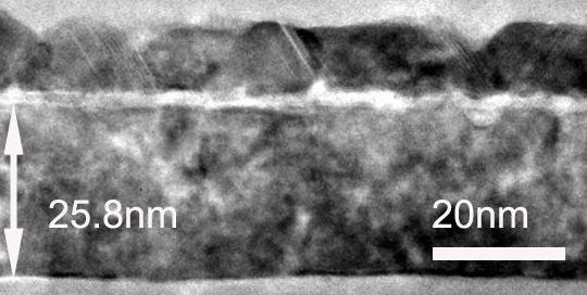
16 Intensity (arb. units) FePt (001) Low Temperature Growth of FePt on CrRu FePt (002) + (200) CrRu (200) FePt (003) (e) (d) (c) (b) Momentum transfer, q (Å -1 ) (a) Magnetisation (emu/cc) Magnetisation (emu/cc) out-of-plane in-plane (a) Applied Field (koe) out-of-plane in-plane 150 C 350 C (c) Applied Field (koe) Magnetisation (emu/cc) K u (x10 7 erg/cc) out-of-plane in-plane (b) Applied Field (koe) H c K u 200 C Deposition temperature ( C) Hc (Oe) FePt (20 nm) Pt (2 nm) CrRu (30nm) Perpendicular anisotropic FePt with high K u and was successfully fabricated at temperature below 350 C, far below the 600 C phase transformation temperature to obtain L1 0 phase of FePt by other methods Glass substrate 15
17 Initial Layer Growth in FePt Perpendicular Media In perpendicular recording media, it has long been discovered that an initial growth layer or also known as nucleation layer or dead layer of low M s and low K u Formed in the magnetic layer during the early film growth stage regardless of whether on top of an underlayer or on substrates. The formation of the initial growth layer was attributed to the poor easy axis orientation in the initial stage of the film growth The initial growth layer resulted in the decrease of measured H c and S of the magnetic film Solution: Introduce buffer layer The purpose of the buffer layer (immiscible with underlayer and recording layer) is to block diffusion from the underlayer and promotes heteroepitaxial growth of the L1 0 phase 2 nm Pt buffer was introduced between CrRu underlayer and FePt magnetic layer 16
18 Effect of Pt Buffer Layer on Crystallographic Properties FePt (001) Pt (200) FePt (002) + (200) 20 nm CrRu (200) (d) FePt (001) FePt (002) + (200) 20 nm CrRu (200) (d) Intensity (arb. units) 10 nm 5 nm 3 nm (c) (b) (a) Intensity (arb. units) 10 nm 5 nm 3 nm (c) (b) (a) Momentum transfer, q (Å -1 ) FePt on 2 nm Pt buffer layer Momentum transfer, q (Å -1 ) FePt on CrRu underlayer 17
19 Hysteresis Loops of FePt on Pt buffer layer and CrRu underlayer Magnetisation (emu/cc) Magnetisation (emu/cc) out-of-plane in-plane Applied Field (koe) out-of-plane in-plane Applied Field (koe) (a) (c) Magnetisation (emu/cc) Magnetisation (emu/cc) out-of-plane in-plane Applied Field (koe) out-of-plane in-plane (b) (d) Applied Field (koe) Magnetisation (emu/cc) Magnetisation (emu/cc) out-of-plane in-plane (a) Applied Field (koe) out-of-plane in-plane Applied Field (koe) (c) Magnetisation (emu/cc) Magnetisation (emu/cc) out-of-plane in-plane Applied Field (koe) out-of-plane in-plane (b) Applied Field (koe) (d) FePt on 2 nm Pt buffer layer FePt on CrRu underlayer 18
20 Evaluation of t initial by zero M s Method Segment, n FePt film thickness from interface (nm), bottom up M s(n), on CrRu underlayer M s(n), on Pt buffer layer emu/cc 732 emu/cc emu/cc 602 emu/cc emu/cc 599 emu/cc emu/cc 481 emu/cc M s x t FePt (x10 3 emu/cc x nm) without Pt buffer layer t initial = 1.4 nm (a) t FePt (nm) M s x t FePt (x10 3 emu/cc x nm) 16 with Pt buffer layer t initial = 0.8 nm (b) t FePt (nm) 19
21 Evaluation of t initial by zero K u Method x t FePt (10 8 erg/cc x nm) K u effective N d =0 N d =4π K grain u = 2.75 x 10 7 erg/cc t initial = 3.16nm N d = 4π K grain = 2.36 x 10 7 erg/cc u t initial = 3.20nm N d = t FePt (nm) It is very difficult to accurately determine the demagnetisation factor of the film 20
22 Change of M s and K u over FePt film thickness Bulk FePt region Low M s region Pt buffer layer CrRu underlayer Low K u region Magnetisation (emu/cc) out-of-plane in-plane 2 nm FePt on Pt buffer layer is soft magnetic Applied Field (koe) 21

23 FePt 5 nm Cr 90 Ru 10 22

24 FePt Pt 23
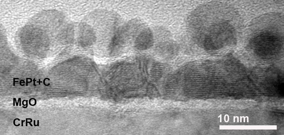
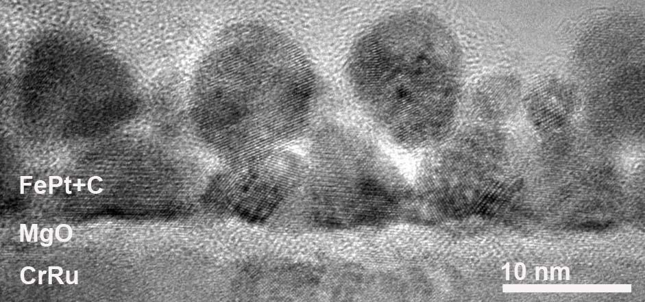
25 New intermediate layer? 1. The interface between FePt and Pt is shaper than that between FePt and CrRu. 2. The initial growth layer thickness estimated by K u model is larger than that estimated by M s, suggesting that there were structural defects existing at the interface which resulted in small anisotropy. But M s does not change due to the structure defect 3. In order to further reduce the initial growth layer thickness, new intermediate layer with suitable crystallographic structure, more difficult to diffuse, is required Solution: MgO was proposed as the buffer layer since sputter deposited MgO formed the (200) texture due to the lowest surface energy plane, and the MgO (200) texture can heteroepitaxially induce the fct-fept (001) texture. 24
26 Advantages of using MgO as buffer layer: Immiscible with FePt recording layer and CrRu underlayer Lattice relationship: MgO (100)<001> FePt (001)<100>, mismatch of 8.66%. Lattice strain maintained Motivation: Advantages of MgO Buffer Layer To study interfacial effects of MgO layer on texture and magnetic properties of FePt as FePt fabrication is carried out at elevated temperature. Interface roughness is expected to change with temperature. a a = nm a Mg 2+ O 2- a 25
 and FePt (001) planes are parallel to the film")
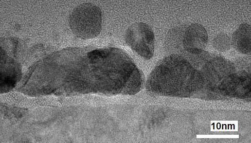
27 HRTEM image of 2 nm MgO deposited at 50 C MgO layer appeared continuous MgO-FePt interface also well-defined MgO (200) and FePt (001) planes are parallel to the film plane 26
 and (001) oriented grains identified,")
28 HRTEM image of 2 nm MgO deposited at 350 C Island-like growth of MgO layer, rough interface FePt (111) and (001) oriented grains identified, defect 27
29 M a g n e t ic p r o p e r t ie s ( M g O d e p o s it e d a t 5 0 C ) (a ) (a ) s h o w s o u t-o f-p la n e a n d in -p la n e lo o p s o f F e P t film w h e n M g O is 4 n m S h o w s p e rp e n d ic u la r a n is o tro p y a n d in c re a s e s w ith in c re a s in g M g O th ic k n e s s 28

30 M a g n e t ic p r o p e r t ie s ( M g O d e p o s it e d a t C ) Is o tro p ic m a g n e tiz a tio n w h e n M g O is 1 n m S h o w s p e rp e n d ic u la r a n is o tro p y w ith in c re a s in g M g O th ic k n e s s, fro m 4 n m H c h ig h e r th a n w h e n M g O d e p o s ite d a t 5 0 C, d u e to d e fe c ts 29
31 Summary of effect of MgO deposition temperature and thickness on film properties MgO layer 50 C <4nm 4nm Continuous Continuous 350 C <4nm 4nm Island-like Continuous MgO-FePt Interface Mostly smooth Smooth Rough Rough and Smooth Dominant FePt texture (001) (001) (111) (001) Anisotropy Perpendicular Perpendicular Isotropic Perpendicular 30
32 Reduction of Initial Growth Layer Thickness by MgO Buffer Layer 7.0 M s x t FePt (x10 3 emu/cc x nm) t initial = 0.6 nm t FePt (nm) 31
33 XRD spectra of 12 nm FePt film deposited at various temperatures 400 C 350 C 300 C 280 C Dominant FePt (001) orientation even at 280 C FePt (001) integrated peak intensity increased with deposition temperature Slight shift of broad peak (45-50 ) to higher angle increase in chemical ordering 32
34 Magnetic properties of 12 nm FePt film deposited at various temperatures 280 C 300 C 350 C 400 C Out-of-plane anisotropic even at 280 C Significant increase in H c with increasing temperature to 400 C 33
 10 vol.% C Normalized Kerr 0.5 0.0-0.5-1.0 5-10 -5 0 5 10 Applied field (koe) 20 vol.")
35 Plan View TEM Images of FePt Doped with Carbon 1.0 out-of-plane Nomalized Kerr Applied Field (koe) 10 vol.% C Normalized Kerr Applied field (koe) 20 vol.% C 34 4


 deposited @350oC.")

36 5 nm 7.5 nm 10 nm 15 nm 5 nm 20 nm 30 nm 20 nm TEM images of 5 to 30 nm thick FePt:C films (15 vol.% C) FePt:C grain growth observation: It confirms the proposed two-step growth model. 10 nm 35 35


37 Microstructure of FePt+C on Pt buffer layer C C C C C Continuous FePt 5nm FePt Pt layer fcc-fept C fct-fept C fcc-fept fcc-fept fct-fept CrRu glass Continuous FePt layer Pt CrRu Model proposed 15nm FePt C FePt C FePt Glass/CrRu/Pt Glass/CrRu/Pt 36
 How about oxide underlayer? MgO (1.")
38 Thin film growth modes Layer by layer growth due to almost similar surface energy of Pt layer and FePt layer (2.9 J/m 2 ) How about oxide underlayer? MgO (1.1 J/m 2 ) Interface interaction between oxide and metal should be higher than between that of metal and metal 37
39 Microstructure of FePt+ x vol%c on MgO buffer layer pure 20% 15% 25% 38

40 Columnar structure of FePt+ x vol%c on MgO buffer layer 2-layer microstructure not favorable for recording application. Adatom mobility of Fe and Pt on substrate were reduced by increasing deposition rate and formed small grain size. Well-isolated FePt-C grains of size about 7.5 nm formed on MgO buffer layer. 1 J.S. Chen et al., Appl. Phys. Lett. 91, (2007) 2 J.S. Chen et al., Appl. Phys. Lett. 90, , (2007) 39
41 Summary Lattice strain induced ordering aided in the reduction of FePt ordering temperature to 350 C and below Buffer layer based on oxide material (MgO) played an important role in lowering the deposition temperature while still keeping chemical ordering high Columnar structure of C doped FePt successfully fabricated 40
Perpendicular Magnetic Multilayers for Advanced Memory Application
 Perpendicular Magnetic Multilayers for Advanced Memory Application Sangmun Oh; Zheng Gao Kochan Ju; Lijie Guan HGST Wafer Development Team 2012 HGST, a Western Digital company 2012 HGST, a Western Digital
GRADED MEDIA: Towards to more than 1 Tbit/in 2 magnetic recording. Dr. D. Niarchos. Th. Speliotis V. Alexandrakis G. Giannopoulos
 IMS, NCSR Demokritos Athens, Greece www.teramagstor.eu GRADED MEDIA: Towards to more than 1 Tbit/in 2 magnetic recording Dr. D. Niarchos Th. Speliotis V. Alexandrakis G. Giannopoulos CAN YOU IMAGINE ~7
Structures of AlN/VN superlattices with different AlN layer thicknesses
 Structures of AlN/VN superlattices with different AlN layer thicknesses Quan Li a) Department of Physics, The Chinese University of Hong Kong, Shatin, New Territory, Hong Kong I.W. Kim, S.A. Barnett, and
Session 1A4a AC Transport, Impedance Spectra, Magnetoimpedance
 Session 1A4a AC Transport, Impedance Spectra, Magnetoimpedance Magneto-impedance of [Co 40Fe 40B 20/Cu] Multilayer Films S. U. Jen, T. Y. Chou, C. K. Lo,.................................................................
Thin Film Scattering: Epitaxial Layers
 Thin Film Scattering: Epitaxial Layers 6th Annual SSRL Workshop on Synchrotron X-ray Scattering Techniques in Materials and Environmental Sciences: Theory and Application May 29-31, 2012 Thin films. Epitaxial
6.8 Magnetic in-plane anisotropy of epitaxially grown Fe-films on vicinal Ag(001) and Au(001) with different miscut orientations
 and Au(001) with different miscut orientations") C. Epitaxial Growth 6.8 Magnetic in-plane anisotropy of epitaxially grown Fe-films on vicinal Ag(001) and Au(001) with different miscut orientations M. Rickart, A.R. Frank, J. Jorzick, Ch. Krämer, S.O.
C. Epitaxial Growth 6.8 Magnetic in-plane anisotropy of epitaxially grown Fe-films on vicinal Ag(001) and Au(001) with different miscut orientations M. Rickart, A.R. Frank, J. Jorzick, Ch. Krämer, S.O.
Hybrid magnetic/semiconductor spintronic materials and devices
 Journal of Magnetism and Magnetic Materials 00 (2006) 000--000 Hybrid magnetic/semiconductor spintronic materials and devices Y.B. Xu, E. Ahmad, J. S. Claydon, Y.X. Lu, S. S. A. Hassan, I. G. Will and
Nanostructured Engineered Materials With High Magneto-optic Performance For Integrated Photonics Applications
 Edith Cowan University Research Online School of Engineering Publications 28 Nanostructured Engineered Materials With High Magneto-optic Performance For Integrated Photonics Applications Mikhail Vasiliev
Combinatorial RF Magnetron Sputtering for Rapid Materials Discovery: Methodology and Applications
 Combinatorial RF Magnetron Sputtering for Rapid Materials Discovery: Methodology and Applications Philip D. Rack,, Jason D. Fowlkes, and Yuepeng Deng Department of Materials Science and Engineering University
MEDIA TECHNOLOGY Current Status and Future Trends
 MEDIA TECHNOLOGY Current Status and Future Trends Dr. Michael A. Russak President & Chief Technical Officer Komag, Incorporated 1710 Automation Parkway San Jose CA 95131-1873 Presented at the THIC Meeting
Chapter Outline How do atoms arrange themselves to form solids?
 Chapter Outline How do atoms arrange themselves to form solids? Fundamental concepts and language Unit cells Crystal structures Face-centered cubic Body-centered cubic Hexagonal close-packed Close packed
Magnetostriction Effect of Amorphous CoFeB Thin Films and. Application in Spin Dependent Tunnel Junctions
 Magnetostriction Effect of Amorphous CoFeB Thin Films and Application in Spin Dependent Tunnel Junctions Dexin Wang, Cathy Nordman, Zhenghong Qian, James M. Daughton, and John Myers, NVE Corporation, 11409
Fabrication and Properties of Nd(Tb,Dy)Co/Cr Films with Perpendicular Magnetic Anisotropy
Co/Cr Films with Perpendicular Magnetic Anisotropy") Fabrication and Properties of (,Dy)/Cr Films with Perpendicular Magnetic Anisotropy Weiming Cheng 1,2, Xiangshui Miao * 1,2, Junbing Yan 2, Xiaomin Cheng 1,2 1 Department of Electronic cience and Technology,
Fabrication and Properties of (,Dy)/Cr Films with Perpendicular Magnetic Anisotropy Weiming Cheng 1,2, Xiangshui Miao * 1,2, Junbing Yan 2, Xiaomin Cheng 1,2 1 Department of Electronic cience and Technology,
Chapter Outline. How do atoms arrange themselves to form solids?
 Chapter Outline How do atoms arrange themselves to form solids? Fundamental concepts and language Unit cells Crystal structures! Face-centered cubic! Body-centered cubic! Hexagonal close-packed Close packed
Synthetic antiferromagnet with Heusler alloy Co 2 FeAl ferromagnetic layers
 Synthetic antiferromagnet with Heusler alloy Co 2 FeAl ferromagnetic layers X. G. Xu, D. L. Zhang, X. Q. Li, J. Bao, Y. Jiang State Key Laboratory for Advanced Metals and Materials, School of Materials
Effects of Ru and Ag cap layers on microstructure and magnetic properties of FePt ultrathin films
 Liu et al. Nanoscale Research Letters (2015) 10:161 DOI 10.1186/s11671-015-0863-x NANO EXPRESS Open Access Effects of Ru and Ag cap layers on microstructure and magnetic properties of FePt ultrathin films
Magnetic properties and granular structure of CoPtÕB films
 JOURNAL OF APPLIED PHYSICS VOLUME 88, NUMBER 5 1 SEPTEMBER 2000 Magnetic properties and granular structure of CoPtÕB films V. Karanasos, a) I. Panagiotopoulos, and D. Niarchos IMS, NCSR Demokritos, Ag.
Changes in the Magnetic Anisotropy of Co Thin Films on Pt(111) Capped by Ag Overlayers. C. W. Su, H. Y. Ho, C. S. Shern, and R. H.
 Capped by Ag Overlayers. C. W. Su, H. Y. Ho, C. S. Shern, and R. H.") CHINEE JOURNAL OF PHYIC VOL. 41, NO. 5 OCTOBER 2003 Changes in the Magnetic Anisotropy of Co Thin Films on Pt(111) Capped by Ag Overlayers C. W. u, H. Y. Ho, C.. hern, and R. H. Chen Department of Physics,
CHINEE JOURNAL OF PHYIC VOL. 41, NO. 5 OCTOBER 2003 Changes in the Magnetic Anisotropy of Co Thin Films on Pt(111) Capped by Ag Overlayers C. W. u, H. Y. Ho, C.. hern, and R. H. Chen Department of Physics,
9/28/2013 9:26 PM. Chapter 3. The structure of crystalline solids. Dr. Mohammad Abuhaiba, PE
 Chapter 3 The structure of crystalline solids 1 2 Why study the structure of crystalline solids? Properties of some materials are directly related to their crystal structure. Significant property differences
Anomaly of Film Porosity Dependence on Deposition Rate
 Anomaly of Film Porosity Dependence on Deposition Rate Stephen P. Stagon and Hanchen Huang* Department of Mechanical Engineering, University of Connecticut, Storrs, CT 06269 J. Kevin Baldwin and Amit Misra
Effect of high annealing temperature on giant tunnel magnetoresistance ratio of. CoFeB/MgO/CoFeB magnetic tunnel junctions
 Effect of high annealing temperature on giant tunnel magnetoresistance ratio of CoFeB/MgO/CoFeB magnetic tunnel junctions J. Hayakawa 1,2, S. Ikeda 2, Y. M. Lee 2, F. Matsukura 2, and H. Ohno 2 1. Hitachi,
Co-Evolution of Stress and Structure During Growth of Polycrystalline Thin Films
 Co-Evolution of Stress and Structure During Growth of Polycrystalline Thin Films Carl V. Thompson and Hang Z. Yu* Dept. of Materials Science and Engineering MIT, Cambridge, MA, USA Effects of intrinsic
9/16/ :30 PM. Chapter 3. The structure of crystalline solids. Mohammad Suliman Abuhaiba, Ph.D., PE
 Chapter 3 The structure of crystalline solids 1 Mohammad Suliman Abuhaiba, Ph.D., PE 2 Home Work Assignments HW 1 2, 7, 12, 17, 22, 29, 34, 39, 44, 48, 53, 58, 63 Due Sunday 17/9/2015 3 Why study the structure
Fundamental concepts and language Unit cells Crystal structures! Face-centered cubic! Body-centered cubic! Hexagonal close-packed Close packed
 Fundamental concepts and language Unit cells Crystal structures! Face-centered cubic! Body-centered cubic! Hexagonal close-packed Close packed crystal structures Density computations Crystal structure
Nd-Fe-B permanent magnets. M. J. O Shea. Kansas State University
 Nd-Fe-B permanent magnets Return to main webpage of mick O Shea M. J. O Shea Kansas State University mjoshea@phys.ksu.edu If you cannot get the papers connected to this work, please e-mail me for a copy
Magnetism of MnBi-Based Nanomaterials
 University of Nebraska - Lincoln DigitalCommons@University of Nebraska - Lincoln Ralph Skomski Publications Research Papers in Physics and Astronomy 7-2013 Magnetism of MnBi-Based Nanomaterials Parashu
Preparation and structural characterization of thin-film CdTe/CdS heterojunctions
 JOURNAL OF OPTOELECTRONICS AND ADVANCED MATERIALS Vol. 8, No., June 006, p. 96-940 Preparation and structural characterization of thin-film CdTe/ heterojunctions I. SALAORU a, P. A. BUFFAT b, D. LAUB b,
LOW transition noise sputtered tape media that can be
 IEEE TRANSACTIONS ON MAGNETICS, VOL. 43, NO. 8, AUGUST 2007 3497 Co Alloy-SiO 2 Granular-Type Longitudinal Media for Sputtered Tape Applications Hwan-Soo Lee 1, Takanori Sato 2, Hiroaki Ono 2, Lin Wang
M agnetic tunnel junctions (MTJs) with ferromagnetic electrodes possessing perpendicular magnetic
 with ferromagnetic electrodes possessing perpendicular magnetic") OPEN SUBJECT AREAS: INFORMATION STORAGE MAGNETIC PROPERTIES AND MATERIALS Received 20 March 2014 Accepted 14 July 2014 Published 31 July 2014 Correspondence and requests for materials should be addressed
OPEN SUBJECT AREAS: INFORMATION STORAGE MAGNETIC PROPERTIES AND MATERIALS Received 20 March 2014 Accepted 14 July 2014 Published 31 July 2014 Correspondence and requests for materials should be addressed
Rietveld refinement of ZrSiO 4 : application of a phenomenological model of anisotropic peak width
 Rietveld refinement of ZrSiO 4 : application of a phenomenological model of anisotropic peak width A. Sarkar, P. Mukherjee, P. Barat Variable Energy Cyclotron Centre 1/A Bidhan Nagar, Kolkata 700064, India
Hf Doping Effect on Hard Magnetism of Nanocrystalline Zr18-x HfxCo82 Ribbons
 University of Nebraska - Lincoln DigitalCommons@University of Nebraska - Lincoln Ralph Skomski Publications Research Papers in Physics and Astronomy 7-2013 Hf Doping Effect on Hard Magnetism of Nanocrystalline
80 Development of REBa2Cu3Ox Coated Conductor on Textured Metal Substrate
 ELECTRIC WIRE & CABLE, ENERGY Development of REBa2Cu3Ox Coated Conductor on Textured Metal Substrate Yuki SHINGAI*, Tatsuoki NAGAISHI, Masaya KONISHI, Hajime OTA, Takahiro TANEDA and Kazuya OHMATSU Sumitomo
LORENTZ TRANSMISSION ELECTRON MICROSCOPY INVESTIGATION OF MAGNETICALLY PATTERNED Co/Pt MULTILAYERS
 LORENTZ TRANSMISSION ELECTRON MICROSCOPY INVESTIGATION OF MAGNETICALLY PATTERNED Co/Pt MULTILAYERS G.J. KUSINSKI 1,2, K.M. KRISHNAN 2, D. WELLER 3, B.D. TERRIS 3, L. FOLKS 3, A.J. KELLOCK 3, J.E.E. BAGLIN
Lawrence Berkeley National Laboratory Lawrence Berkeley National Laboratory
 Lawrence Berkeley National Laboratory Lawrence Berkeley National Laboratory Title Lorentz transmission electron microscopy investigation of magnetically patterned Co/Pt multilayers Permalink https://escholarship.org/uc/item/6gr7d3t3
Exchange Bias and Bi- stable Magneto- Resistance States in Amorphous TbFeCo and TbSmFeCo Thin Films
 Exchange Bias and Bi- stable Magneto- Resistance States in Amorphous TbFeCo and TbSmFeCo Thin Films Chung Ting (Marco) Ma University of Virginia 4th Year Seminar 1 Outline Background Why are we interested
Thin Film Characterizations Using XRD The Cases of VO2 and NbTiN
 Thin Film Characterizations Using XRD The Cases of VO2 and NbTiN A thesis submitted in partial fulfillment of the requirement for the degree of Bachelor of Arts / Science in Physics from The College of
ARTICLE IN PRESS. Journal of Magnetism and Magnetic Materials
 Journal of Magnetism and Magnetic Materials 322 (2010) 315 321 Contents lists available at ScienceDirect Journal of Magnetism and Magnetic Materials journal homepage: www.elsevier.com/locate/jmmm Transmission
SEMATECH Symposium Korea 2012 Practical Analysis Techniques of Nanostructured Semiconductors by Electron Microscopy
 SEMATECH Symposium Korea 2012 Practical Analysis Techniques of Nanostructured Semiconductors by Electron Microscopy Jun-Mo Yang, Ph.D. Measurement & Analysis Team National NanoFab Center, Korea Introduction
Packing of atoms in solids
 MME131: Lecture 6 Packing of atoms in solids A. K. M. B. Rashid Professor, Department of MME BUET, Dhaka Today s topics Atomic arrangements in solids Points, directions and planes in unit cell References:
Advanced Magnetic Force Microscopy for High Resolution magnetic imaging
 Advanced Magnetic Force Microscopy for High Resolution magnetic imaging M. Ranjbar 1, 2, S.N. Piramanayagam 1*, R. Sbiaa 1, T.C. Chong 1, 2, I. Okamoto 3 1 Data Storage Institute, A*STAR (Agency for Science
Transmission Electron Microscopy (TEM) Prof.Dr.Figen KAYA
 Prof.Dr.Figen KAYA") Transmission Electron Microscopy (TEM) Prof.Dr.Figen KAYA Transmission Electron Microscope A transmission electron microscope, similar to a transmission light microscope, has the following components along
Transmission Electron Microscopy (TEM) Prof.Dr.Figen KAYA Transmission Electron Microscope A transmission electron microscope, similar to a transmission light microscope, has the following components along
8. Epitaxy. - Extended single-crystal film formation on top of a crystalline substrate
 8. Epitaxy 1. Introduction επι(epi placed or resting upon) ταξιζ(taxis arrangement) - Extended single-crystal film formation on top of a crystalline substrate - Homoepitaxy : Film and substrate are the
Magnetic Force Microscopy: nanoscale magnetic imaging and lithography
 NTEGRA Aura Magnetic Force Microscopy: nanoscale magnetic imaging and lithography The principle of Magnetic Force Microscopy (MFM) is based on the detection of the interaction between the sample and a
Soft Magnetic Properties of Nanocystalline Fe Si B Nb Cu Rod Alloys Obtained by Crystallization of Cast Amorphous Phase
 Materials Transactions, Vol. 43, No. 9 (2002) pp. 2337 to 2341 c 2002 The Japan Institute of Metals EXPRESS REGULAR ARTICLE Soft Magnetic Properties of Nanocystalline Fe Si B Nb Cu Rod Alloys Obtained
X-RAY DIFFRACTION CHARACTERIZATION OF MULTILAYER EPITAXIAL THIN FILMS DEPOSITED ON (0001) SAPPHIRE
 SAPPHIRE") The Rigaku Journal Vol. 13/No. 1/ 1996 CONTRIBUTED PAPERS X-RAY DIFFRACTION CHARACTERIZATION OF MULTILAYER EPITAXIAL THIN FILMS DEPOSITED ON (0001) SAPPHIRE THOMAS N. BLANTON AND LIANG-SUN HUNG Imaging
The Rigaku Journal Vol. 13/No. 1/ 1996 CONTRIBUTED PAPERS X-RAY DIFFRACTION CHARACTERIZATION OF MULTILAYER EPITAXIAL THIN FILMS DEPOSITED ON (0001) SAPPHIRE THOMAS N. BLANTON AND LIANG-SUN HUNG Imaging
arxiv: v1 [cond-mat.mtrl-sci] 19 Dec 2016
![arxiv: v1 [cond-mat.mtrl-sci] 19 Dec 2016](/thumbs/72/67071303.jpg "arxiv: v1 [cond-mat.mtrl-sci] 19 Dec 2016") How to enable bulk-like martensitic transformation in epitaxial films arxiv:1612.06077v1 [cond-mat.mtrl-sci] 19 Dec 2016 Marius Wodniok, 1 Niclas Teichert, 1,a) Lars Helmich, 1 and Andreas Hütten 1 Center
How to enable bulk-like martensitic transformation in epitaxial films arxiv:1612.06077v1 [cond-mat.mtrl-sci] 19 Dec 2016 Marius Wodniok, 1 Niclas Teichert, 1,a) Lars Helmich, 1 and Andreas Hütten 1 Center
Structure of silica glasses (Chapter 12)
") Questions and Problems 97 Glass Ceramics (Structure) heat-treated so as to become crystalline in nature. The following concept map notes this relationship: Structure of noncrystalline solids (Chapter 3)
Questions and Problems 97 Glass Ceramics (Structure) heat-treated so as to become crystalline in nature. The following concept map notes this relationship: Structure of noncrystalline solids (Chapter 3)
Point Defects. Vacancies are the most important form. Vacancies Self-interstitials
 Grain Boundaries 1 Point Defects 2 Point Defects A Point Defect is a crystalline defect associated with one or, at most, several atomic sites. These are defects at a single atom position. Vacancies Self-interstitials
Energy and Packing. Materials and Packing
 Energy and Packing Non dense, random packing Energy typical neighbor bond length typical neighbor bond energy r Dense, regular packing Energy typical neighbor bond length typical neighbor bond energy r
Available online at ScienceDirect. Materials Today: Proceedings 2 (2015 )
") Available online at www.sciencedirect.com ScienceDirect Materials Today: Proceedings 2 (2015 ) 5582 5586 International Conference on Solid State Physics 2013 (ICSSP 13) Thickness dependent optimization
Available online at www.sciencedirect.com ScienceDirect Materials Today: Proceedings 2 (2015 ) 5582 5586 International Conference on Solid State Physics 2013 (ICSSP 13) Thickness dependent optimization
Texture and properties - II
 Texture and properties - II Texture and Hall-Petch strength The Hall-Petch equation 0 k d - ½ where, 0 = k = d = lattice frictional stress locking parameter average grain size modifies for textured polycrystals
Interfacial reaction mechanisms and the structure of moving heterophase boundaries during pyrochlore- and spinel-forming solid state reactions
 Dietrich Hesse, Stephan Senz Max-Planck-Institut für Mikrostrukturphysik, Halle (Saale), Germany Interfacial reaction mechanisms and the structure of moving heterophase boundaries during pyrochlore- and
Carbon nanostructures. (http://www.mf.mpg.de/de/abteilungen/schuetz/index.php?lang=en&content=researchtopics&type=specific&name=h2storage)
") Carbon nanostructures (http://www.mf.mpg.de/de/abteilungen/schuetz/index.php?lang=en&content=researchtopics&type=specific&name=h2storage) 1 Crystal Structures Crystalline Material: atoms arrange into a
Carbon nanostructures (http://www.mf.mpg.de/de/abteilungen/schuetz/index.php?lang=en&content=researchtopics&type=specific&name=h2storage) 1 Crystal Structures Crystalline Material: atoms arrange into a
Performance at Wafer-Scale
 Supporting Information Self-Assembling VO 2 Nanonet with High Switching Performance at Wafer-Scale Jiasong Zhang, Haibo Jin*, Zhuo Chen, Maosheng Cao, Pengwan Chen, Yankun Dou, Yongjie Zhao, Jingbo Li*
Supplementary Figure S1 Crystal structure of the conducting filaments in sputtered SiO 2
 Supplementary Figure S1 Crystal structure of the conducting filaments in sputtered SiO 2 based devices. (a) TEM image of the conducting filament in a SiO 2 based memory device used for SAED analysis. (b)
CHAPTER 5 IMPERFECTIONS IN SOLIDS PROBLEM SOLUTIONS
 CHAPTER 5 IMPERFECTIONS IN SOLIDS PROBLEM SOLUTIONS Vacancies and Self-Interstitials 5.1 Calculate the fraction of atom sites that are vacant for copper at its melting temperature of 1084 C (1357 K). Assume
Ab-initio Calculation of Structural and Magnetic Properties of Annealed Cu 2 MnAl Heusler Alloy
 International Conference on Material Science and Application (ICMSA 2015) Ab-initio Calculation of Structural and Magnetic Properties of Annealed Cu 2 MnAl Heusler Alloy Hang SHI 1,a, Xin WANG 2,b*, Nan
Materials Issues in Fatigue and Fracture. 5.1 Fundamental Concepts 5.2 Ensuring Infinite Life 5.3 Failure 5.4 Summary
 Materials Issues in Fatigue and Fracture 5.1 Fundamental Concepts 5.2 Ensuring Infinite Life 5.3 Failure 5.4 Summary 1 A simple view of fatigue 1. Will a crack nucleate? 2. Will it grow? 3. How fast will
Phase Transitions Module γ-2: VSM study of Curie Temperatures 1 Instructor: Silvija Gradečak
 3.014 Materials Laboratory November 13 th 18 th, 2006 Lab week 3 Phase Transitions Module γ-2: VSM study of Curie Temperatures 1 Instructor: Silvija Gradečak Objectives: a) Understand magnetic and thermal
Anisotropic Mechanical Properties of Pr(Co,In) 5 -type Compounds and Their Relation to Texture Formation in Die-upset Magnets
 5 -type Compounds and Their Relation to Texture Formation in Die-upset Magnets") Journal of Magnetics 16(3), 220-224 (2011) http://dx.doi.org/10.4283/jmag.2011.16.3.220 Anisotropic Mechanical Properties of Pr(Co,In) 5 -type Compounds and Their Relation to Texture Formation in Die-upset
Journal of Magnetics 16(3), 220-224 (2011) http://dx.doi.org/10.4283/jmag.2011.16.3.220 Anisotropic Mechanical Properties of Pr(Co,In) 5 -type Compounds and Their Relation to Texture Formation in Die-upset
Development of low roughness, low resistance bottom electrodes for tunnel junction devices
 Development of low roughness, low resistance bottom electrodes for tunnel junction devices Designing and assembly of a new annealing setup for 150mm wafers David Filipe Coelho de Almeida Aurélio Setembro
Soft Magnetic Nanocrystalline Alloys for High Temperature Applications. 1. U.S. Naval Research Laboratory, Materials Physics Branch, Code 6340,
 Soft Magnetic Nanocrystalline Alloys for High Temperature Applications Matthew A. Willard 1, Frank Johnson 2, John H. Claassen 1, Rhonda M. Stroud 1, Michael E. McHenry 2, and Vincent G. Harris 1 1. U.S.
Silver Diffusion Bonding and Layer Transfer of Lithium Niobate to Silicon
 Chapter 5 Silver Diffusion Bonding and Layer Transfer of Lithium Niobate to Silicon 5.1 Introduction In this chapter, we discuss a method of metallic bonding between two deposited silver layers. A diffusion
Growth and Doping of SiC-Thin Films on Low-Stress, Amorphous Si 3 N 4 /Si Substrates for Robust Microelectromechanical Systems Applications
 Journal of ELECTRONIC MATERIALS, Vol. 31, No. 5, 2002 Special Issue Paper Growth and Doping of SiC-Thin Films on Low-Stress, Amorphous Si 3 N 4 /Si Substrates for Robust Microelectromechanical Systems
Phase Transformations in Metals Tuesday, December 24, 2013 Dr. Mohammad Suliman Abuhaiba, PE 1
 Ferrite - BCC Martensite - BCT Fe 3 C (cementite)- orthorhombic Austenite - FCC Chapter 10 Phase Transformations in Metals Tuesday, December 24, 2013 Dr. Mohammad Suliman Abuhaiba, PE 1 Why do we study
Properties of TiN thin films grown on SiO 2 by reactive HiPIMS
 Properties of TiN thin films grown on SiO 2 by reactive HiPIMS Friðrik Magnus 1, Árni S. Ingason 1, Ólafur B. Sveinsson 1, S. Shayestehaminzadeh 1, Sveinn Ólafsson 1 and Jón Tómas Guðmundsson 1,2 1 Science
HiPIMS Technology: advantages and disadvantages
 Vacuum plasma technology HiPIMS Technology: advantages and disadvantages Cr - DC Cr - HiPIMS Alessandro Patelli alessandro.patelli@venetonanotech.it Outline 1. What is HiPIMS Ti target surface 2. What
Magnetic Shape Memory Alloys
 Sebastian Fähler and Kathrin Dörr, IFW Dresden Magnetic Shape Memory Alloys www.adaptamat.com Magnetically Induced Martensite (MIM) Magnetically Induced Reorientation (MIR) Requirements for actuation Exotic
Ba-hexaferrite films for next generation microwave devices invited
 JOURNAL OF APPLIED PHYSICS 99, 08M911 2006 Ba-hexaferrite films for next generation microwave devices invited V. G. Harris, a Zhaohui Chen, Yajie Chen, Soack Yoon, Tomokuza Sakai, Anton Gieler, Aria Yang,
SPI Supplies Brand MgO Magnesium Oxide Single Crystal Substrates, Blocks, and Optical Components
 SPI Supplies Brand MgO Magnesium Oxide Single Crystal Substrates, Blocks, and Optical Components Used by high temperature thin film superconductor researchers worldwide! Purity better than 99.9%! Choose
Introduction. 1. Sputtering process, target materials and their applications
 Sputtering is widely used in the production of electronic devices such as liquid crystal displays (LCDs), optical media, magnetic media and semiconductors. The Kobelco Research Institute, Inc. has been
Excimer Laser Annealing of Hydrogen Modulation Doped a-si Film
 Materials Transactions, Vol. 48, No. 5 (27) pp. 975 to 979 #27 The Japan Institute of Metals Excimer Laser Annealing of Hydrogen Modulation Doped a-si Film Akira Heya 1, Naoto Matsuo 1, Tadashi Serikawa
Recrystallization in CdTe/CdS
 Thin Solid Films 361±362 (2000) 420±425 www.elsevier.com/locate/tsf Recrystallization in CdTe/CdS A. Romeo, D.L. BaÈtzner, H. Zogg, A.N. Tiwari* Thin Film Physics Group, Institute of Quantum Electronics,
Strengthening Mechanisms
 Strengthening Mechanisms The ability of a metal/ alloy to plastically deform depends on the ability of dislocations to move. Strengthening techniques rely on restricting dislocation motion to render a
ALD and CVD of Copper-Based Metallization for. Microelectronic Fabrication. Department of Chemistry and Chemical Biology
 ALD and CVD of Copper-Based Metallization for Microelectronic Fabrication Yeung Au, Youbo Lin, Hoon Kim, Zhengwen Li, and Roy G. Gordon Department of Chemistry and Chemical Biology Harvard University Introduction
Adhesive strength of interfaces between bcc and fcc Fe and transition metal carbides: effect of misfit dislocations on structure and bonding
 Adhesive strength of interfaces between bcc and fcc Fe and transition metal carbides: effect of misfit dislocations on structure and bonding Oleg Y. Kontsevoi 1, Arthur J. Freeman 1,2, and Gregory B. Olson
Effect of Li Addition on Synthesis of Mg-Ti BCC Alloys by means of Ball Milling
 Materials Transactions, Vol. 48, No. 2 (07) pp. 121 to 126 #07 The Japan Institute of Metals Effect of Li Addition on Synthesis of - BCC Alloys by means of Ball Milling Kohta Asano, Hirotoshi Enoki and
This journal is The Royal Society of Chemistry S 1
 2013 S 1 Thermochemical analysis on the growth of NiAl 2 O 4 rods Sang Sub Kim, a Yong Jung Kwon, b Gunju Sun, a Hyoun Woo Kim,* b and Ping Wu* c a Department of Materials Science and Engineering, Inha
Relation Between Internal Stress and Surface Roughness of Titanium Nitride Films Deposited by HCD Ion Plating
 No.22,28 65 Relation Between Internal Stress and Surface Roughness of Titanium Nitride Films Deposited by HCD Ion Plating Itsuo Ishigami Ken-ichi Miura Hideaki Hoshino Tomoyuki Mizukoshi (28 6 17 ) An
Part IV. Solid-solid transformations I
 Part IV : Solid-Solid Phase Transformations I Module 1 : Precipitation Part IV. Solid-solid transformations I In this part, we discuss a few of the important solid-solid transformations, namely, precipitation,
Effects of Lead on Tin Whisker Elimination
 Effects of Lead on Tin Whisker Elimination Wan Zhang and Felix Schwager Rohm and Haas Electronic Materials Lucerne, Switzerland inemi Tin Whisker Workshop at ECTC 0 May 30, 2006, in San Diego, CA Efforts
Structural and Magnetic Properties of Neodymium - Iron - Boron Clusters
 University of Nebraska - Lincoln DigitalCommons@University of Nebraska - Lincoln Mechanical (and Materials) Engineering -- Dissertations, Theses, and Student Research Mechanical & Materials Engineering,
Enhanced magneto-optical effect due to interface alloy formation in Co±Pt (1 1 1) ultrathin lms upon thermal annealing
 ultrathin lms upon thermal annealing") Applied Surface Science 169±170 (2001) 231±235 Enhanced magneto-optical effect due to interface alloy formation in Co±Pt (1 1 1) ultrathin lms upon thermal annealing M.-T. Lin a,*, C.C. Kuo a, J.W. Ho
Applied Surface Science 169±170 (2001) 231±235 Enhanced magneto-optical effect due to interface alloy formation in Co±Pt (1 1 1) ultrathin lms upon thermal annealing M.-T. Lin a,*, C.C. Kuo a, J.W. Ho
3.40 Sketch within a cubic unit cell the following planes: (a) (01 1 ) (b) (112 ) (c) (102 ) (d) (13 1) Solution
 (01 1 ) (b) (112 ) (c) (102 ) (d) (13 1) Solution") 3.40 Sketch within a cubic unit cell the following planes: (a) (01 1 ) (b) (11 ) (c) (10 ) (d) (13 1) The planes called for are plotted in the cubic unit cells shown below. 3.41 Determine the Miller indices
3.40 Sketch within a cubic unit cell the following planes: (a) (01 1 ) (b) (11 ) (c) (10 ) (d) (13 1) The planes called for are plotted in the cubic unit cells shown below. 3.41 Determine the Miller indices
Figure 2.3 (cont., p. 60) (e) Block diagram of Pentium 4 processor with 42 million transistors (2000). [Courtesy Intel Corporation.
 (e) Block diagram of Pentium 4 processor with 42 million transistors (2000). [Courtesy Intel Corporation.") Figure 2.1 (p. 58) Basic fabrication steps in the silicon planar process: (a) oxide formation, (b) selective oxide removal, (c) deposition of dopant atoms on wafer, (d) diffusion of dopant atoms into exposed
Figure 2.1 (p. 58) Basic fabrication steps in the silicon planar process: (a) oxide formation, (b) selective oxide removal, (c) deposition of dopant atoms on wafer, (d) diffusion of dopant atoms into exposed
Chapter 10, Phase Transformations
 Chapter Outline: Phase Transformations Heat Treatment (time and temperature) Microstructure Kinetics of phase transformations Homogeneous and heterogeneous nucleation Growth, rate of the phase transformation
Three-dimensional epitaxy: Thermodynamic stability range of coherent germanium nanocrystallites in silicon
 Three-dimensional epitaxy: Thermodynamic stability range of coherent germanium nanocrystallites in silicon S. Balasubramanian, a) G. Ceder, and K. D. Kolenbrander Department of Materials Science and Engineering,
Phase Transitions in Iron-Platinum
 Phase Transitions in Iron-Platinum Hannah E. Herde Department of Physics, Wellesley College, Wellesley, MA 02481 Regan Lab Department of Physics and Astronomy, University of California - Los Angeles, Los
Monolithic Microphotonic Optical Isolator
 Monolithic Microphotonic Optical Isolator Lei Bi, Juejun Hu, Dong Hun Kim, Peng Jiang, Gerald F Dionne, Caroline A Ross, L.C. Kimerling Dept. of Materials Science and Engineering Massachusetts Institute
The influence of the internal microstructure on the surface parameters of polycrystalline thin films
 The influence of the internal microstructure on the surface parameters of polycrystalline thin films C. Eisenmenger-Sittner and A. Bergauer Institut für Angewandte und Technische Physik, Technische Universität
X-ray Diffraction Study on Structural Characteristics of Pure and Doped Perovskite BaTiO 3
 Egypt. J. Solids, Vol. (31), No. (1), (2008) 55 X-ray Diffraction Study on Structural Characteristics of Pure and Doped Perovskite BaTiO 3 F. F. Hammad 1, A. K. Mohamed 1 and A. M. El-Shabiny 2 1) Inorganic
Chapter 9 Heat treatment (This chapter covers selective sections in Callister Chap. 9, 10 &11)
") Chapter 9 Heat treatment (This chapter covers selective sections in Callister Chap. 9, 10 &11) Study theme outcomes: After studying this chapter, students should or should be able to: - know and understand
Chapter 9 Heat treatment (This chapter covers selective sections in Callister Chap. 9, 10 &11) Study theme outcomes: After studying this chapter, students should or should be able to: - know and understand
Lecture 22: Integrated circuit fabrication
 Lecture 22: Integrated circuit fabrication Contents 1 Introduction 1 2 Layering 4 3 Patterning 7 4 Doping 8 4.1 Thermal diffusion......................... 10 4.2 Ion implantation.........................
Materials Characterization
 Materials Characterization C. R. Abernathy, B. Gila, K. Jones Cathodoluminescence (CL) system FEI Nova NanoSEM (FEG source) with: EDAX Apollo silicon drift detector (TE cooled) Gatan MonoCL3+ FEI SEM arrived
University of Pretoria Z Tang (2006) Chapter 8 Studies of acicular ferrite by thin foil TEM
 Chapter 8 Studies of acicular ferrite by thin foil TEM") 8.2 Two types of acicular ferrite 8.2.1 Structure with parallel laths There appeared to be two types of acicular ferrite laths that were observed in those alloys cooled with a rapid cooling rate of 47
8.2 Two types of acicular ferrite 8.2.1 Structure with parallel laths There appeared to be two types of acicular ferrite laths that were observed in those alloys cooled with a rapid cooling rate of 47
Precipitation Hardening. Outline. Precipitation Hardening. Precipitation Hardening
 Outline Dispersion Strengthening Mechanical Properties of Steel Effect of Pearlite Particles impede dislocations. Things that slow down/hinder/impede dislocation movement will increase, y and TS And also
modeling of grain growth and coarsening in multi-component alloys
 Quantitative phase-field modeling of grain growth and coarsening in multi-component alloys N. Moelans (1), L. Vanherpe (2), A. Serbruyns (1) (1), B. B. Rodiers (3) (1) Department of metallurgy and materials
X ray diffraction in materials science
 X ray diffraction in materials science Goals: Use XRD spectra to determine the orientation of single crystals and preferred orientations in a thin film. Understand how grain size and strain affect the
Strain-induced anomalous magnetoresistance effect in ultrathin manganite films and nanostructures
 Strain-induced anomalous magnetoresistance effect in ultrathin manganite films and nanostructures Qi Li Pennsylvania State University Department of Physics University Park, PA 16802 Collaborators: Y. F.