Process Integration. NMOS Generic NMOS Process Flow. CMOS - The MOSIS Process Flow
|
|
|
- Gavin Harvey Murphy
- 6 years ago
- Views:
Transcription
1 Process Integration Self-aligned Techniques LOCOS- self-aligned channel stop Self-aligned Source/Drain Lightly Doped Drain (LDD) Self-aligned silicide (SALICIDE) Self-aligned oxide gap MEMS Release Techniques Sacrificial Layer Removal Substrate Undercut Advance Techniques Twin Well CMOS Retrograde Wells SOI CMOS NMOS Generic NMOS Process Flow. CMOS - The MOSIS Process Flow
2 Self-aligned channel stop with Local Oxidation (LOCOS) LOCOS Process Flow Si 3 N 4 CVD pad oxide Si
3 Si B + channel stop dose implant ~10 13 /cm 2 B thermal oxidation (high temperature) FOX p p Self-aligned channel stop
4 Comment: Channel Inversion * If a poly or metal line lies on top of the FOX, they will form a parasitic MOS structure.if these lines carrying a high voltage, they may create an inversion layer of free electrons at the Si substrate and shorts out neighboring devices. The relatively highly doped Si underneath (the channel stop ) raises the threshold voltage needed for the inversion metal Device 1 Device 2 SiO 2 Electron Inversion Layer p-si 4
5 Comments : Non self-aligned alternative: P.R. B SiO 2 3 SiO2 P + P Si + P + P + Disadvantages 1) Two lithography steps 2) Channel stop doping not aligned with field oxide
6 Self-aligned Source and Drain Perfect Alignment poly-si gate As + n +. n + n + Off Alignment. n + As + * The n+ S/D always follows gate
7 Comment: Non self-aligned Alternative. n + n 1 +. n + n + 2 n + Channel not linked to S/D Stray capacitance. n + Solution Use gate overlap to avoid offset error. Disadvantages: Two lithography steps, excess gate overlap capacitance
8 Lightly Doped Source/Drain MOSFET (LDD) CVD oxide spacer n + n n n + SiO 2 p-sub The n-pockets (LDD) doped to medium conc (~1E18) is to smear out the strong E-field bewteen the channel and heavily doped n+ S/D. Less hot-carrier generation. 8
9 LDD Process Flow n implant for LDD CVD conformal deposition SiO 2 CVD SiO 2 SiO 2 Directional RIE of CVD Oxide 9
10 0.05µm 0.25µm Spacer left when CVD SiO 2 is just cleared on flat region. n n n + implant n n n + n + 10
11 Self-Aligned Silicide Process (SALICIDE) poly-gate TiSi 2 (metal) n + n + * Metal silicides are metallic. Lower the sheet resistance of S/D and the poly-gate 11
12 SALICIDE Process Flow oxide spacer SiO 2 n + n + 12
13 Ti deposition Ti SiO 2 n + n + Si heat treatment ( > 700 o C) Ti TiSi 2 Ti Ti Ti Ti + 2Si TiSi will not react with 2 SiO 2. Selective etch to remove unreacted Ti only 13
14 Self-aligned Oxide Gap DRAM structure ( MOSFET with a capacitor) Thermal Oxide grown conformallay on poly-i small oxide spacing < 30nm poly-i n+ substrate MOSFET poly-i poly-ii poly-ii Gate oxide MOS Capacitor V (plate) inversion charge layer NOTE For a small spacing between poly-i and poly-ii, inversion charges between MOSFET and Capacitor are electrically linked. No need for a separate n+ island. 14


15 Process Flow of MEMS Rotating Mechanisms In-Plane Movement Microturbine Engine 15


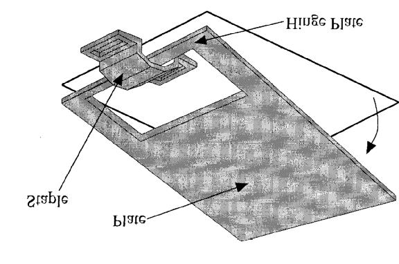
16 Process Flow for a Hinge Structure Out-of-plane Movement 16
")
17 Layout of Thermal Bimorph Actuator (See 143 Lab Manual for details) 17
18 After Patterning Poly-Si ( Mask #2) Top View Aluminum Poly Si Oxide Si substrate Al-Poly contact Cross Section 18
19 After Patterning Intermediate Oxide ( Mask #3, Contact-Hole Cut) Top View Aluminum Poly Si Oxide Si substrate Al-Poly contact Cross Section 19
20 After Aluminum patterning (Mask #4) To contact pad Top View Aluminum Poly Si Oxide Si substrate Al-Poly contact Cross Section 20
21 After XeF2 selective etching of Si Substrate (Final Structure) To contact pad Top View Aluminum Poly Si Oxide Si substrate Al-Poly contact Cross Section 21
22 A Generic NMOS Process Flow Substrate Boron doped (100)Si Resistivity= 20 Ω-cm Thermal Oxidation ~100Å pad oxide CVD Si 3 N 4 ~ 0.1 um Lithography Pattern Field Oxide Regions RIE removal of Nitride and pad oxide Channel Stop Implant: 3x10 12 B/cm 2 60keV Thermal Oxidation to grow 0.45um oxide Wet Etch Nitrdie and pad oxide Ion Implant for Threshold Voltage control 8x10 11 B/cm 2 35keV Thermal Oxidation To grow 250Å gate oxide LPCVD Poly-Si ~ 0.35um Dope Poly-Si to n+ with Phosphorus Diffusion source 22
23 Lithography Poly-Si Gate pattern RIE Poly-Si gate Source /Drain Implantation ~ As/cm 2 80keV Thermal Oxidation Grow ~0.1um oxide on poly-si And source/drian LPCVD SiO2 ~0.35um Lithography Contact Window pattern RIE removal of CVD oxide and thermal oxide Sputter Deposit Al metal ~0.7um Lithography Al interconnect pattern RIE etch of Al metallization Sintering at ~400 o C in H2 ambient to improve contact resistance and to reduce oxide interface charge 23
24 NMOS Structure Generic NMOS Process Flow Boron-doped Si 20 Ω -cm <100> active device ~5 µm p-si <100> 500µm


25 P.R. SiO 2 Si nitride nitride P.R. B : keV 12 / cm 2 SiO 2 0.1µm Si / cm 3

26 Fox p + p B 5 10 / cm 35keV Fox p + p +


27 Resist As+ 80keV, /cm 2 n + n + Thermal oxide n + n +


28 Al CVD oxide intermediate oxide n + n + Al H 2 anneal ~ 400 o C n + n + Si/SiO 2 Interface States Passivation
Lecture 030 Integrated Circuit Technology - I (5/8/03) Page 030-1
 Page 030-1") Lecture 030 Integrated Circuit Technology - I (5/8/03) Page 030-1 LECTURE 030 INTEGRATED CIRCUIT TECHNOLOGY - I (References [7,8]) Objective The objective of this presentation is: 1.) Illustrate integrated
Lecture 030 Integrated Circuit Technology - I (5/8/03) Page 030-1 LECTURE 030 INTEGRATED CIRCUIT TECHNOLOGY - I (References [7,8]) Objective The objective of this presentation is: 1.) Illustrate integrated
3.155J / 6.152J Micro/Nano Processing Technology TAKE-HOME QUIZ FALL TERM 2005
 3.155J / 6.152J Micro/Nano Processing Technology TAKE-HOME QUIZ FALL TERM 2005 1) This is an open book, take-home quiz. You are not to consult with other class members or anyone else. You may discuss the
Isolation Technology. Dr. Lynn Fuller
 ROCHESTER INSTITUTE OF TECHNOLOGY MICROELECTRONIC ENGINEERING Isolation Technology Dr. Lynn Fuller Motorola Professor 82 Lomb Memorial Drive Rochester, NY 14623-5604 Tel (585) 475-2035 Fax (585) 475-5041
VLSI Systems and Computer Architecture Lab
 ΚΥΚΛΩΜΑΤΑ VLSI Πανεπιστήμιο Ιωαννίνων CMOS Technology Τμήμα Μηχανικών Η/Υ και Πληροφορικής 1 From the book: An Introduction ti to VLSI Process By: W. Maly ΚΥΚΛΩΜΑΤΑ VLSI Διάρθρωση 1. N well CMOS 2. Active
EE 434 Lecture 9. IC Fabrication Technology
 EE 434 Lecture 9 IC Fabrication Technology Quiz 7 The layout of a film resistor with electrodes A and B is shown. If the sheet resistance of the film is 40 /, determine the resistance between nodes A and
Silicon Wafer Processing PAKAGING AND TEST
 Silicon Wafer Processing PAKAGING AND TEST Parametrical test using test structures regularly distributed in the wafer Wafer die test marking defective dies dies separation die fixing (not marked as defective)
VLSI INTRODUCTION P.VIDYA SAGAR ( ASSOCIATE PROFESSOR) Department of Electronics and Communication Engineering, VBIT
 Department of Electronics and Communication Engineering, VBIT") VLSI INTRODUCTION P.VIDYA SAGAR ( ASSOCIATE PROFESSOR) contents UNIT I INTRODUCTION: Introduction to IC Technology MOS, PMOS, NMOS, CMOS & BiCMOS technologies. BASIC ELECTRICAL PROPERTIES : Basic Electrical
VLSI INTRODUCTION P.VIDYA SAGAR ( ASSOCIATE PROFESSOR) contents UNIT I INTRODUCTION: Introduction to IC Technology MOS, PMOS, NMOS, CMOS & BiCMOS technologies. BASIC ELECTRICAL PROPERTIES : Basic Electrical
EE 560 FABRICATION OF MOS CIRCUITS. Kenneth R. Laker, University of Pennsylvania
 1 EE 560 FABRICATION OF MOS CIRCUITS 2 CMOS CHIP MANUFACTRING STEPS Substrate Wafer Wafer Fabrication (diffusion, oxidation, photomasking, ion implantation, thin film deposition, etc.) Finished Wafer Wafer
Lecture 19 Microfabrication 4/1/03 Prof. Andy Neureuther
 EECS 40 Spring 2003 Lecture 19 Microfabrication 4/1/03 Prof. ndy Neureuther How are Integrated Circuits made? Silicon wafers Oxide formation by growth or deposition Other films Pattern transfer by lithography
CMOS Manufacturing Process
 CMOS Manufacturing Process CMOS Process A Modern CMOS Process gate-oxide TiSi 2 AlCu Tungsten SiO 2 n+ p-well p-epi poly n-well p+ SiO 2 p+ Dual-Well Trench-Isolated CMOS Process Circuit Under Design V
Figure 2.3 (cont., p. 60) (e) Block diagram of Pentium 4 processor with 42 million transistors (2000). [Courtesy Intel Corporation.
 (e) Block diagram of Pentium 4 processor with 42 million transistors (2000). [Courtesy Intel Corporation.") Figure 2.1 (p. 58) Basic fabrication steps in the silicon planar process: (a) oxide formation, (b) selective oxide removal, (c) deposition of dopant atoms on wafer, (d) diffusion of dopant atoms into exposed
Figure 2.1 (p. 58) Basic fabrication steps in the silicon planar process: (a) oxide formation, (b) selective oxide removal, (c) deposition of dopant atoms on wafer, (d) diffusion of dopant atoms into exposed
Semiconductor Manufacturing Technology. IC Fabrication Process Overview
 Semiconductor Manufacturing Technology Michael Quirk & Julian Serda October 00 by Prentice Hall Chapter 9 IC Fabrication Process Overview /4 Objectives After studying the material in this chapter, you
Surface micromachining and Process flow part 1
 Surface micromachining and Process flow part 1 Identify the basic steps of a generic surface micromachining process Identify the critical requirements needed to create a MEMS using surface micromachining
Manufacturing Process
 Digital Integrated Circuits A Design Perspective Jan M. Rabaey Anantha Chandrakasan Borivoje Nikolic Manufacturing Process July 30, 2002 1 CMOS Process 2 A Modern CMOS Process gate-oxide TiSi 2 AlCu Tungsten
VLSI Technology. By: Ajay Kumar Gautam
 By: Ajay Kumar Gautam Introduction to VLSI Technology, Crystal Growth, Oxidation, Epitaxial Process, Diffusion Process, Ion Implantation, Lithography, Etching, Metallization, VLSI Process Integration,
CMOS FABRICATION. n WELL PROCESS
 CMOS FABRICATION n WELL PROCESS Step 1: Si Substrate Start with p- type substrate p substrate Step 2: Oxidation Exposing to high-purity oxygen and hydrogen at approx. 1000 o C in oxidation furnace SiO
Process Flow in Cross Sections
 Process Flow in Cross Sections Process (simplified) 0. Clean wafer in nasty acids (HF, HNO 3, H 2 SO 4,...) --> wear gloves! 1. Grow 500 nm of SiO 2 (by putting the wafer in a furnace with O 2 2. Coat
EE40 Lec 22. IC Fabrication Technology. Prof. Nathan Cheung 11/19/2009
 Suggested Reading EE40 Lec 22 IC Fabrication Technology Prof. Nathan Cheung 11/19/2009 300mm Fab Tour http://www-03.ibm.com/technology/manufacturing/technology_tour_300mm_foundry.html Overview of IC Technology
HOMEWORK 4 and 5. March 15, Homework is due on Monday March 30, 2009 in Class. Answer the following questions from the Course Textbook:
 HOMEWORK 4 and 5 March 15, 2009 Homework is due on Monday March 30, 2009 in Class. Chapter 7 Answer the following questions from the Course Textbook: 7.2, 7.3, 7.4, 7.5, 7.6*, 7.7, 7.9*, 7.10*, 7.16, 7.17*,
Development of a Deep-Submicron CMOS Process for Fabrication of High Performance 0.25 mm Transistors
 Development of a Deep-Submicron CMOS Process for Fabrication of High Performance 0.25 mm Transistors Michael Aquilino M.S. Thesis Defense Department May 19, 2006 Motivation o Enable the department to continue
6.777J/2.732J Design and Fabrication of Microelectromechanical Devices Spring Term Solution to Problem Set 2 (16 pts)
") 6.777J/2.732J Design and Fabrication of Microelectromechanical Devices Spring Term 2007 By Brian Taff (Adapted from work by Feras Eid) Solution to Problem Set 2 (16 pts) Issued: Lecture 4 Due: Lecture
6.777J/2.732J Design and Fabrication of Microelectromechanical Devices Spring Term 2007 By Brian Taff (Adapted from work by Feras Eid) Solution to Problem Set 2 (16 pts) Issued: Lecture 4 Due: Lecture
National Semiconductor LM2672 Simple Switcher Voltage Regulator
 Construction Analysis National Semiconductor LM2672 Simple Switcher Voltage Regulator Report Number: SCA 9712-570 Global Semiconductor Industry the Serving Since 1964 17350 N. Hartford Drive Scottsdale,
Lecture 22: Integrated circuit fabrication
 Lecture 22: Integrated circuit fabrication Contents 1 Introduction 1 2 Layering 4 3 Patterning 7 4 Doping 8 4.1 Thermal diffusion......................... 10 4.2 Ion implantation.........................
Fabrication and Layout
 Fabrication and Layout Kenneth Yun UC San Diego Adapted from EE271 notes, Stanford University Overview Semiconductor properties How chips are made Design rules for layout Reading Fabrication: W&E 3.1,
EEC 118 Lecture #5: MOS Fabrication. Rajeevan Amirtharajah University of California, Davis Jeff Parkhurst Intel Corporation
 EEC 118 Lecture #5: MOS Fabrication Rajeevan Amirtharajah University of California, Davis Jeff Parkhurst Intel Corporation Announcements Lab 3 this week, report due next week HW 3 due this Friday at 4
Interconnects OUTLINE
 Interconnects 1 Interconnects OUTLINE 1. Overview of Metallization 2. Introduction to Deposition Methods 3. Interconnect Technology 4. Contact Technology 5. Refractory Metals and their Silicides Reading:
EE 330 Fall Ruden Michael. Al Kaabi Humaid. Archer Tyler. Hafeez Mustafa. Mullen Taylor. Thedens Peter. Cao Khoi.
 1 2 5 6 3 4 8 7 1 2 3 4 5 6 ROW EE 330 Fall 2017 9 10 Al Kaabi Humaid Alegria Francisco Allison Trenton Alva Caroline Archer Tyler Bahashwan Abdullah Betke Jarrett Chun Junho Davidson Caleb Faronbi Matthew
VLSI Technology Dr. Nandita Dasgupta Department of Electrical Engineering Indian Institute of Technology, Madras
 VLSI Technology Dr. Nandita Dasgupta Department of Electrical Engineering Indian Institute of Technology, Madras Lecture - 33 Problems in LOCOS + Trench Isolation and Selective Epitaxy So, we are discussing
Semiconductor Physics Course Final Presentation CMOS Fabrication by Özgür Çobanoğlu (Turin, 2006)
") Semiconductor Physics Course Final Presentation CMOS Fabrication by Özgür Çobanoğlu (Turin, 2006) 1 Outline Sections and Contents of the Presentation What is MOS? How does MOS behave in low level? A useful
Semiconductor Physics Course Final Presentation CMOS Fabrication by Özgür Çobanoğlu (Turin, 2006) 1 Outline Sections and Contents of the Presentation What is MOS? How does MOS behave in low level? A useful
Lezioni di Tecnologie e Materiali per l Elettronica
 Lezioni di Tecnologie e Materiali er l Elettronica Danilo Manstretta danilo.manstretta@univ.it microlab.univ.it Outline Passive comonents Resistors Caacitors Inductors Printed circuits technologies Materials
Lecture 5. SOI Micromachining. SOI MUMPs. SOI Micromachining. Silicon-on-Insulator Microstructures. Agenda:
 EEL6935 Advanced MEMS (Spring 2005) Instructor: Dr. Huikai Xie SOI Micromachining Agenda: SOI Micromachining SOI MUMPs Multi-level structures Lecture 5 Silicon-on-Insulator Microstructures Single-crystal
Intel Pentium Processor W/MMX
 Construction Analysis Intel Pentium Processor W/MMX Report Number: SCA 9706-540 Global Semiconductor Industry the Serving Since 1964 15022 N. 75th Street Scottsdale, AZ 85260-2476 Phone: 602-998-9780 Fax:
EE C245 ME C218 Introduction to MEMS Design Fall 2011
 Lecture Outline EE C245 ME C218 Introduction to MEMS Design Fall 2011 Prof. Clark T.-C. Nguyen Dept. of Electrical Engineering & Computer Sciences University of California at Berkeley Berkeley, CA 94720
Metallization. Typical current density ~10 5 A/cm 2 Wires introduce parasitic resistance and capacitance
 Metallization Interconnects Typical current density ~10 5 A/cm 2 Wires introduce parasitic resistance and capacitance RC time delay Inter-Metal Dielectric -Prefer low dielectric constant to reduce capacitance
Ajay Kumar Gautam [VLSI TECHNOLOGY] VLSI Technology for 3RD Year ECE/EEE Uttarakhand Technical University
![Ajay Kumar Gautam [VLSI TECHNOLOGY] VLSI Technology for 3RD Year ECE/EEE Uttarakhand Technical University](/thumbs/75/72824557.jpg "Ajay Kumar Gautam [VLSI TECHNOLOGY] VLSI Technology for 3RD Year ECE/EEE Uttarakhand Technical University") 2014 Ajay Kumar Gautam [VLSI TECHNOLOGY] VLSI Technology for 3RD Year ECE/EEE Uttarakhand Technical University Page1 Syllabus UNIT 1 Introduction to VLSI Technology: Classification of ICs, Scale of integration,
2014 Ajay Kumar Gautam [VLSI TECHNOLOGY] VLSI Technology for 3RD Year ECE/EEE Uttarakhand Technical University Page1 Syllabus UNIT 1 Introduction to VLSI Technology: Classification of ICs, Scale of integration,
Lecture 7 CMOS MEMS. CMOS MEMS Processes. CMOS MEMS Processes. Why CMOS-MEMS? Agenda: CMOS MEMS: Fabrication. MEMS structures can be made
 EEL6935 Advanced MEMS (Spring 2005) Instructor: Dr. Huikai Xie CMOS MEMS Agenda: Lecture 7 CMOS MEMS: Fabrication Pre-CMOS Intra-CMOS Post-CMOS Deposition Etching Why CMOS-MEMS? Smart on-chip CMOS circuitry
Fabrication and Layout
 ECEN454 Digital Integrated Circuit Design Fabrication and Layout ECEN 454 3.1 A Glimpse at MOS Device Polysilicon Aluminum ECEN 475 4.2 1 Material Classification Insulators Glass, diamond, silicon oxide
Surface Micromachining
 Surface Micromachining Outline Introduction Material often used in surface micromachining Material selection criteria in surface micromachining Case study: Fabrication of electrostatic motor Major issues
CMOS Manufacturing process. Circuit designer. Design rule set. Process engineer. Set of optical masks. Fabrication process.
 CMOS Manufacturing process Circuit design Set of optical masks Fabrication process Circuit designer Design rule set Process engineer All material: Chap. 2 of J. Rabaey, A. Chandrakasan, B. Nikolic, Digital
Silicon Oxides: SiO 2
 Silicon Oxides: SiO 2 Uses: diffusion masks surface passivation gate insulator (MOSFET) isolation, insulation Formation: grown / native thermal: highest quality anodization deposited: C V D, evaporate,
Metallization. Typical current density ~105 A/cm2 Wires introduce parasitic resistance and capacitance
 Metallization Interconnects Typical current density ~105 A/cm2 Wires introduce parasitic resistance and capacitance RC time delay Inter-Metal Dielectric -Prefer low dielectric constant to reduce capacitance
5.8 Diaphragm Uniaxial Optical Accelerometer
 5.8 Diaphragm Uniaxial Optical Accelerometer Optical accelerometers are based on the BESOI (Bond and Etch back Silicon On Insulator) wafers, supplied by Shin-Etsu with (100) orientation, 4 diameter and
Rockwell R RF to IF Down Converter
 Construction Analysis Rockwell R6732-13 RF to IF Down Converter Report Number: SCA 9709-552 Global Semiconductor Industry the Serving Since 1964 17350 N. Hartford Drive Scottsdale, AZ 85255 Phone: 602-515-9780
4/10/2012. Introduction to Microfabrication. Fabrication
 Introduction to Microfabrication Fabrication 1 MEMS Fabrication Flow Basic Process Flow in Micromachining Nadim Maluf, An introduction to Microelectromechanical Systems Engineering 2 Thin Film Deposition
2015 EE410-LOCOS 0.5µm Poly CMOS Process Run Card Lot ID:
 STEP 0.00 - PHOTOMASK #0- ZERO LEVEL MARKS Starting materials is n-type silicon (5-10 ohm-cm). Add four test wafers labeled T1-T4. T1 and T2 will travel with the device wafers and get all of the processing
Advanced CMOS Process Technology Part 3 Dr. Lynn Fuller
 MICROELECTRONIC ENGINEERING ROCHESTER INSTITUTE OF TECHNOLOGY Part 3 Dr. Lynn Fuller Webpage: http://people.rit.edu/lffeee Electrical and Microelectronic Engineering Rochester Institute of Technology 82
Historical Development. Babbage s second computer. Before the digital age
 Historical Development To fully appreciate the computers of today, it is helpful to understand how things got the way they are The evolution of computing machinery has taken place over several centuries
Workfunction Tuning for Single-Metal Dual-Gate With Mo and NiSi Electrodes
 tivation Workfunction Tuning for ngle-metal Dual-Gate With and i Electrodes poly- Gate Gate depletion effect -Effective oxide thickness increase Metal Gate o gate depletion effect K.Sano, M.Hino, and K.Shibahara
ELEC 3908, Physical Electronics, Lecture 4. Basic Integrated Circuit Processing
 ELEC 3908, Physical Electronics, Lecture 4 Basic Integrated Circuit Processing Lecture Outline Details of the physical structure of devices will be very important in developing models for electrical behavior
Cost of Integrated Circuits
 Cost of IC Design 1 Cost of Integrated Circuits NRE (Non-Recurrent Engineering) costs fixed design time and effort, mask generation independent of sales volume / number of products one-time cost factor
Motorola PC603R Microprocessor
 Construction Analysis Motorola PC603R Microprocessor Report Number: SCA 9709-551 Global Semiconductor Industry the Serving Since 1964 17350 N. Hartford Drive Scottsdale, AZ 85255 Phone: 602-515-9780 Fax:
1 Thin-film applications to microelectronic technology
 1 Thin-film applications to microelectronic technology 1.1 Introduction Layered thin-film structures are used in microelectronic, opto-electronic, flat panel display, and electronic packaging technologies.
Schottky-Barrier-Height Modulation of Ni Silicide/Si Contacts by Insertion of Thin Er or Pt Layers
 Schottky-Barrier-Height Modulation of Ni Silicide/Si Contacts by Insertion of Thin Er or Pt Layers Yoshihisa Ohishi 1, Kohei Noguchi 1, Kuniyuki Kakushima 2, Parhat Ahmet 1, Kazuo Tsutsui 2, Nobuyuki Sugii
Micro-Scale Engineering I Microelectromechanical Systems (MEMS) Y. C. Lee
 Y. C. Lee") Micro-Scale Engineering I Microelectromechanical Systems (MEMS) Y. C. Lee Department of Mechanical Engineering University of Colorado Boulder, CO 80309-0427 leeyc@colorado.edu September 2, 2008 1 Three
Micro-Scale Engineering I Microelectromechanical Systems (MEMS) Y. C. Lee Department of Mechanical Engineering University of Colorado Boulder, CO 80309-0427 leeyc@colorado.edu September 2, 2008 1 Three
2. High Efficiency Crystalline Si Solar Cells
 2 High Efficiency Crystalline Si Solar Cells Students: Karthick Murukesan, Sandeep S S, Meenakshi Bhaisare, Bandana Singha, Kalaivani S and Ketan Warikoo Faculty members: Anil Kottantharayil, B M Arora,
Tri-Gate Transistor Architecture with High-k Gate Dielectrics, Metal Gates and Strain Engineering
 Tri-Gate Transistor Architecture with High-k Gate Dielectrics, Metal Gates and Strain Engineering Jack Kavalieros, Brian Doyle, Suman Datta, Gilbert Dewey, Mark Doczy, Ben Jin, Dan Lionberger, Matthew
Silicon Manufacturing
 Silicon Manufacturing Group Members Young Soon Song Nghia Nguyen Kei Wong Eyad Fanous Hanna Kim Steven Hsu th Fundamental Processing Steps 1.Silicon Manufacturing a) Czochralski method. b) Wafer Manufacturing
FABRICATION ENGINEERING MICRO- NANOSCALE ATTHE AND. Fourth Edition STEPHEN A. CAMPBELL. of Minnesota. University OXFORD UNIVERSITY PRESS
 AND FABRICATION ENGINEERING ATTHE MICRO- NANOSCALE Fourth Edition STEPHEN A. CAMPBELL University of Minnesota New York Oxford OXFORD UNIVERSITY PRESS CONTENTS Preface xiii prrt i OVERVIEW AND MATERIALS
Lecture 2. Fabrication and Layout
 Lecture 2 Fabrication and Layout Mark Horowitz Modified by Azita Emami Computer Systems Laboratory Stanford University azita@stanford.edu 1 Overview Reading W&E 3.1(scan), 3.2.1, 3.3.1 - Fabrication W&E
Radiation Tolerant Isolation Technology
 Radiation Tolerant Isolation Technology Background The following contains a brief description of isolation technologies used for radiation hardened integrated circuits. The technologies mentioned are junction
Ion Implantation Most modern devices doped using ion implanters Implant dopants by accelerating individual atoms (ions) Ionize gas sources (single +,
 Ionize gas sources (single +,") Ion Implantation Most modern devices doped using ion implanters Implant dopants by accelerating individual atoms (ions) Ionize gas sources (single +, 2+ or 3+ ionization) Use analyzer to selection charge/mass
Ion Implantation Most modern devices doped using ion implanters Implant dopants by accelerating individual atoms (ions) Ionize gas sources (single +, 2+ or 3+ ionization) Use analyzer to selection charge/mass
CHAPTER 2 - CMOS TECHNOLOGY
 CMOS Analog Circuit Design Page 2.0-1 CHAPTER 2 - CMOS TECHNOLOGY Chapter Outline 2.1 Basic MOS Semiconductor Fabrication Processes 2.2 CMOS Technology 2.3 PN Junction 2.4 MOS Transistor 2.5 Passive Components
Lecture 4. Oxidation (applies to Si and SiC only) Reading: Chapter 4
 Reading: Chapter 4") Lecture 4 Oxidation (applies to Si and SiC only) Reading: Chapter 4 Introduction discussion: Oxidation: Si (and SiC) Only The ability to grow a high quality thermal oxide has propelled Si into the forefront
Lecture 4 Oxidation (applies to Si and SiC only) Reading: Chapter 4 Introduction discussion: Oxidation: Si (and SiC) Only The ability to grow a high quality thermal oxide has propelled Si into the forefront
Advancing RIT to Submicron Technology: Design and Fabrication of O.5~j,m N-channel MOS Transistors
 Advancing RIT to Submicron Technology: Design and Fabrication of O.5~j,m N-channel MOS Transistors Ivlichael Aquilino, Student Member, IEEE Absh act The design and fabrication of N-channel MOS transistors
SURFACE MICROMACHINING
 SURFACE MICROMACHINING Features are built up, layer by layer on the surface of a substrate. Surface micromachined devices are much smaller than bulk micromachined components. Nature of deposition process
Isolation of elements
 1 In an IC, devices on the same substrate must be isolated from one another so that there is no current conduction between them. Isolation uses either the junction or dielectric technique or a combination
Modeling of Local Oxidation Processes
 Introduction Isolation Processes in the VLSI Technology Main Aspects of LOCOS simulation Athena Oxidation Models Several Examples of LOCOS structures Calibration of LOCOS effects using VWF Field Oxide
SEMATECH Symposium Korea 2012 Practical Analysis Techniques of Nanostructured Semiconductors by Electron Microscopy
 SEMATECH Symposium Korea 2012 Practical Analysis Techniques of Nanostructured Semiconductors by Electron Microscopy Jun-Mo Yang, Ph.D. Measurement & Analysis Team National NanoFab Center, Korea Introduction
Chapter 2. Density 2.65 g/cm 3 Melting point Young s modulus Tensile strength Thermal conductivity Dielectric constant 3.
 Chapter 2 Thin Film Materials Thin films of Silicon dioxide, Silicon nitride and Polysilicon have been utilized in the fabrication of absolute micro pressure sensor. These materials are studied and discussed
Section 4: Thermal Oxidation. Jaeger Chapter 3. EE143 - Ali Javey
 Section 4: Thermal Oxidation Jaeger Chapter 3 Properties of O Thermal O is amorphous. Weight Density =.0 gm/cm 3 Molecular Density =.3E molecules/cm 3 O Crystalline O [Quartz] =.65 gm/cm 3 (1) Excellent
Electrical Characteristics of Rare Earth (La, Ce, Pr and Tm) Oxides/Silicates Gate Dielectric
 Oxides/Silicates Gate Dielectric") Electrical Characteristics of Rare Earth (La, Ce, Pr and Tm) Oxides/Silicates Gate Dielectric K. Matano 1, K. Funamizu 1, M. Kouda 1, K. Kakushima 2, P. Ahmet 1, K. Tsutsui 2, A. Nishiyama 2, N. Sugii
Electrical Characteristics of Rare Earth (La, Ce, Pr and Tm) Oxides/Silicates Gate Dielectric K. Matano 1, K. Funamizu 1, M. Kouda 1, K. Kakushima 2, P. Ahmet 1, K. Tsutsui 2, A. Nishiyama 2, N. Sugii
Semiconductor Technology
 Semiconductor Technology from A to Z Oxidation www.halbleiter.org Contents Contents List of Figures List of Tables II III 1 Oxidation 1 1.1 Overview..................................... 1 1.1.1 Application...............................
Atomic Layer Deposition(ALD)
") Atomic Layer Deposition(ALD) AlO x for diffusion barriers OLED displays http://en.wikipedia.org/wiki/atomic_layer_deposition#/media/file:ald_schematics.jpg Lam s market-leading ALTUS systems combine CVD
Atomic Layer Deposition(ALD) AlO x for diffusion barriers OLED displays http://en.wikipedia.org/wiki/atomic_layer_deposition#/media/file:ald_schematics.jpg Lam s market-leading ALTUS systems combine CVD
Ion Implantation Most modern devices doped using ion implanters Ionize gas sources (single +, 2+ or 3+ ionization) Accelerate dopant ions to very
 Accelerate dopant ions to very") Ion Implantation Most modern devices doped using ion implanters Ionize gas sources (single +, 2+ or 3+ ionization) Accelerate dopant ions to very high voltages (10-600 KeV) Use analyzer to selection charge/mass
Ion Implantation Most modern devices doped using ion implanters Ionize gas sources (single +, 2+ or 3+ ionization) Accelerate dopant ions to very high voltages (10-600 KeV) Use analyzer to selection charge/mass
Epi Replacement and up to 30% Process Simplification in a CMOS Foundry Environment Using the BILLI Structure
 Epi Replacement and up to 30% Process Simplification in a CMOS Foundry Environment Using the BILLI Structure Martin Teague, Susan Johns, Rob Haase, Paul Jones & Peter Lister Newport Waferfab Limited, Cardiff
ME 141B: The MEMS Class Introduction to MEMS and MEMS Design. Sumita Pennathur UCSB
 ME 141B: The MEMS Class Introduction to MEMS and MEMS Design Sumita Pennathur UCSB Outline today Introduction to thin films Oxidation Deal-grove model CVD Epitaxy Electrodeposition 10/6/10 2/45 Creating
EE-612: Lecture 28: Overview of SOI Technology
 EE-612: Lecture 28: Overview of SOI Technology Mark Lundstrom Electrical and Computer Engineering Purdue University West Lafayette, IN USA Fall 2006 NCN www.nanohub.org Lundstrom EE-612 F06 1 outline 1)
Lecture #9: Active-Matrix LCDs
 Lecture #9: Active-Matrix LCDs Introduction OUTLINE Active-matrix switching elements TFT performance requirements Active matrix processing constraints Amorphous silicon (a-si) TFT technology TFT fabrication
Hitachi A 64Mbit (8Mb x 8) Dynamic RAM
 Dynamic RAM") Construction Analysis Hitachi 5165805A 64Mbit (8Mb x 8) Dynamic RAM Report Number: SCA 9712-565 Global Semiconductor Industry the Serving Since 1964 17350 N. Hartford Drive Scottsdale, AZ 85255 Phone:
Construction Analysis Hitachi 5165805A 64Mbit (8Mb x 8) Dynamic RAM Report Number: SCA 9712-565 Global Semiconductor Industry the Serving Since 1964 17350 N. Hartford Drive Scottsdale, AZ 85255 Phone:
Nonplanar Metallization. Planar Metallization. Professor N Cheung, U.C. Berkeley
 Nonplanar Metallization Planar Metallization Passivation Metal 5 (copper) Metal 3 (copper) Interlevel dielectric (ILD) Via (tungsten) Metal 1 (copper) Tungsten Plug to Si Silicon Caps and Plugs oxide oxide
MOS Gate Dielectrics. Outline
 MOS Gate Dielectrics Outline Scaling issues Technology Reliability of SiO 2 Nitrided SiO 2 High k dielectrics 42 Incorporation of N or F at the Si/SiO 2 Interface Incorporating nitrogen or fluorine instead
CMOS VLSI Design M.Tech. First semester VTU Anil V. Nandi, ECE department, BVBCET, Hubli
 CMOS VLSI Design M.Tech. First semester VTU Anil V. Nandi, ECE department, BVBCET, Hubli-580031. Contents: Semiconductor Technology overview Silicon Growth/Processing,Oxidation, Diffusion, Epitaxy, deposition,
2242 ieee transactions on ultrasonics, ferroelectrics, and frequency control, vol. 52, no. 12, december 2005
 2242 ieee transactions on ultrasonics, ferroelectrics, and frequency control, vol. 52, no. 12, december 2005 Capacitive Micromachined Ultrasonic Transducers: Fabrication Technology Arif Sanlı Ergun, Member,
200mm Next Generation MEMS Technology update. Florent Ducrot
 200mm Next Generation MEMS Technology update Florent Ducrot The Most Exciting Industries on Earth Semiconductor Display Solar 20,000,000x reduction in COST PER TRANSISTOR in 30 years 1 20x reduction in
Section 4: Thermal Oxidation. Jaeger Chapter 3
 Section 4: Thermal Oxidation Jaeger Chapter 3 Properties of O Thermal O is amorphous. Weight Density =.0 gm/cm 3 Molecular Density =.3E molecules/cm 3 O Crystalline O [Quartz] =.65 gm/cm 3 (1) Excellent
Semiconductor Manufacturing Technology. Semiconductor Manufacturing Technology
 Semiconductor Manufacturing Technology Michael Quirk & Julian Serda October 2001 by Prentice Hall Chapter 11 Deposition Film Layers for an MSI Era NMOS Transistor Topside Nitride Pre-metal oxide Sidewall
Dallas Semicoductor DS80C320 Microcontroller
 Construction Analysis Dallas Semicoductor DS80C320 Microcontroller Report Number: SCA 9702-525 Global Semiconductor Industry the Serving Since 1964 15022 N. 75th Street Scottsdale, AZ 85260-2476 Phone:
How To Write A Flowchart
 1 Learning Objectives To learn how you transfer a device concept into a process flow to fabricate the device in the EKL labs You learn the different components that makes up a flowchart; process blocks,
Advanced Gate Stack, Source/Drain, and Channel Engineering for Si-Based CMOS 6: New Materials, Processes, and Equipment
 Advanced Gate Stack, Source/Drain, and Channel Engineering for Si-Based CMOS 6: New Materials, Processes, and Equipment Editors: E. P. Gusev Qualcomm MEMS Technologies San Jose, California, USA D-L. Kwong
Regents of the University of California
 Surface-Micromachining Process Flow Photoresist Sacrificial Oxide Structural Polysilcon Deposit sacrificial PSG: Target = 2 m 1 hr. 40 min. LPCVD @450 o C Densify the PSG Anneal @950 o C for 30 min. Lithography
Lattice isplsi1032e CPLD
 Construction Analysis Lattice isplsi1032e CPLD Report Number: SCA 9612-522 Global Semiconductor Industry the Serving Since 1964 15022 N. 75th Street Scottsdale, AZ 85260-2476 Phone: 602-998-9780 Fax: 602-948-1925
3. Overview of Microfabrication Techniques
 3. Overview of Microfabrication Techniques The Si revolution First Transistor Bell Labs (1947) Si integrated circuits Texas Instruments (~1960) Modern ICs More? Check out: http://www.pbs.org/transistor/background1/events/miraclemo.html
New Materials as an enabler for Advanced Chip Manufacturing
 New Materials as an enabler for Advanced Chip Manufacturing Drive Innovation, Deliver Excellence ASM International Analyst and Investor Technology Seminar Semicon West July 10 2013 Outline New Materials:
Solutions Manual to Accompany
 Solutions Manual to Accompany FUNDAMETALS OF SEMICONDUCTOR FABRICATION G. S. May Motorola Foundation Professor School of Electrical & Computer Engineering Georgia Institute of Technology Atlanta, GA, USA
IEEE TRANSACTIONS ON NUCLEAR SCIENCE, VOL. 55, NO. 4, AUGUST
 IEEE TRANSACTIONS ON NUCLEAR SCIENCE, VOL. 55, NO. 4, AUGUST 2008 1833 Radiation Effects in MOS Oxides James R. Schwank, Fellow, IEEE, Marty R. Shaneyfelt, Fellow, IEEE, Daniel M. Fleetwood, Fellow, IEEE,
INTERCONNECTION, AND CONTACT
 PROCEEDINGS OF THE SYMPOSIA ON RELIABILITY OF SEMICONDUCTOR DEVICES AND INTERCONNECTION AND MULTILEVEL METALLIZATION, INTERCONNECTION, AND CONTACT TECHNOLOGIES Edited by Harzara S. Rathore Hopewell Junction,
Integrated Processes. Lecture Outline
 Integrated Processes Thara Srinivasan Lecture 14 Picture credit: Lemkin et al. Lecture Outline From reader Bustillo, J. et al., Surface micromachining of MEMS, pp. 1556-9. A.E. Franke et al., Polycrystalline
Fabrication Technology
 Fabrication Technology By B.G.Balagangadhar Department of Electronics and Communication Ghousia College of Engineering, Ramanagaram 1 OUTLINE Introduction Why Silicon The purity of Silicon Czochralski
Plasma Etching Rates & Gases Gas ratios affects etch rate & etch ratios to resist/substrate
 Plasma Etching Rates & Gases Gas ratios affects etch rate & etch ratios to resist/substrate Development of Sidewalls Passivating Films Sidewalls get inert species deposited on them with plasma etch Creates
Nanosilicon single-electron transistors and memory
 Nanosilicon single-electron transistors and memory Z. A. K. Durrani (1, 2) and H. Ahmed (3) (1) Electronic Devices and Materials Group, Engineering Department, University of Cambridge, Trumpington Street,