HiPIMS deposition of dense Palladium-Silver films for hydrogen separation
|
|
|
- Gloria Morrison
- 6 years ago
- Views:
Transcription

1 HiPIMS deposition of dense Palladium-Silver films for hydrogen separation S. Fasolin, S. Barison, S. Boldrini, F. Montagner, M. Romano, A. Ferrario, M. Fabrizio, L. Armelao CNR-ICMATE, Corso Stati uniti 4, 35127, Padova - Italy stefano.fasolin@cnr.it
. Pd - FCC a = 0.3890 nm Pd(H) α - FCC a = 0.3895 nm Pd(H) - FCC a = 0.")
2 Palladium-based membranes Pure Palladium exhibit the ability to adsorb hydrogen and to catalyse dehydrogenation from hydrocarbons. Membrane development started with self standing palladium membranes for hydrogen purification (mostly tubular). Pd - FCC a = nm Pd(H) α - FCC a = nm Pd(H) - FCC a = nm PROS - High selectivity/permeability to hydrogen - Working temperature CONS - Embrittlement - Costs
 How to reduce Pd amount and improve stability? 1. Thinner membranes supported onto porous substrates 2.")
3 Palladium-based membranes Hydrogen membrane costs are strictly related to Pd amount. European limits for critical raw materials + US Dep. of Energy cost target -> 1000$/m 2 (film of pure Pd thinner than 3μm) How to reduce Pd amount and improve stability? 1. Thinner membranes supported onto porous substrates 2. Improve stability and reduce Pd amount, introducing elements (Pd alloys or alternatives) Pd 77 Ag 23 Silver stabilize lattice, promoting hydrogen adsorption and diffusion, and lowering the embrittlement temperature. Al 2 O 3 Alumina is a common and cheap oxide, easy to use to obtain porous substrate.
 the target current density can be increased with formation of ultra dense")
4 Hi-PIMS: High-Power Impulse Magnetron Sputtering It is a Physical Vapour Deposition technique derived from Magnetron Sputtering (MS). By using pulse mode (target current pulsed from 1 s to 1s) the target current density can be increased with formation of ultra dense plasma.
 - High degree of ionization (sputtered species) Target material ions can be accelerated")

5 Hi-PIMS: High-Power Impulse Magnetron Sputtering Features: - High power densities (kw/cm 2 ) in short pulses (μs) - High degree of ionization (sputtered species) Target material ions can be accelerated towards the substrate along the field lines Benefits: - Film quality: better adhesion and density, lower defectivity and roughness. - Homogenous deposition onto complex shapes. - Easily scalable for industrial application.

6 Hi-PIMS: High-Power Impulse Magnetron Sputtering DC unit HiPIMS Pulse unit Arc Suppression droplet-free sputtering T pulse and frequency Bias unit Designed to work with generators Hi-pulse Arc Management DC Pulse unit
7 Hi-PIMS parameters Which parameters affect deposition rate and film quality? - Pressure (mainly affect the ions free medium path) - Gas (inert, reactive ) - Type of target (metallic, non metallic, magnetic ) - Type of substrate (conductive, insulating, smooth, rough ) - Power, current, pulses applied to the target - Distance between target and substrate - Bias (acceleration of ions from target to substrate) - Substrate temperature - Deposition time - Sample holder rotation (homogenization)
8 Porous support α-al 2 O 3 + pore former Pore former tested: starch, graphite, poly methyl methacrylate (round shape, average size 1,5 3 7 μm) Ball milling Uniaxial pressure Sintering Surface polishing Cleaning


")
 Maximum")
9 Porous support Surface Cross section Best result: α-al 2 O 3 + PMMA (1,5 μm average size) Open porosity (40 vol%) Maximum pore size about 1 μm


10 Hi-PIMS: planar membranes deposition Argon atmosphere Heated sample holder Rotating sample holder

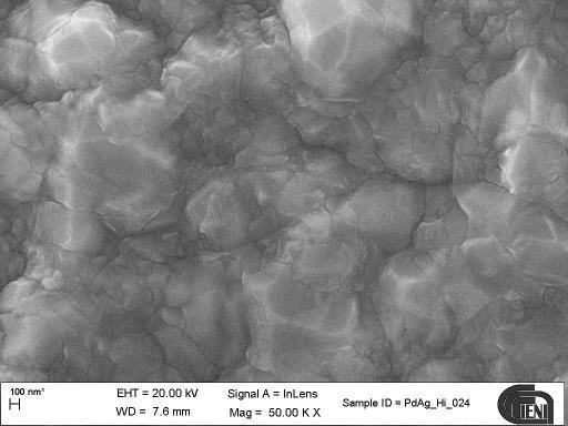
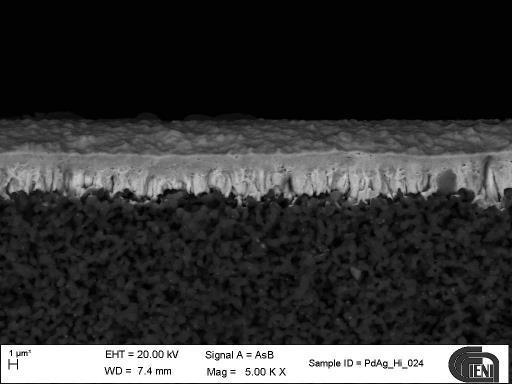
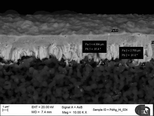
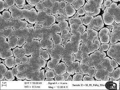
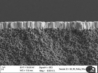
11 Pd 77 Ag 23 membranes: SEM analyses Classic MS Hi-PIMS Classic MS
12 PdAg membranes: XRD and EDS analyses EDS Pd 77% ± 2% Ag 23%± 2%


13 PdAg membranes: permeability test Inox steel Furnace Gas: nitrogen, helium, hydrogen, argon, syngas. Pressure range: from 0,1 to 3 bar over atmospheric pressure; Temperature range: RT-450ºC; PC with Labview controller
14 PdAg membranes: XRD analyses

15 Pd 77 Ag 23 membranes: permeance 400 C = 1,90E-6 mol/m 2 s Pa 350 C = 1,70E-6 mol/m 2 s Pa 300 C = 1,48E-6 mol/m 2 s Pa Literature Permeances Pd 77 Ag 350 C = 1,20E-6 mol/m 2 s Pa Pd 70 Ag 350 C = 2,00E-6 mol/m 2 s Pa
16 Conclusions and perspectives Conclusions - A fine tuning of HiPIMS parameters for insulating and porous substrate coverage were achieved. - Thin and dense Pd 77 Ag 23 films have been deposited onto porous alumina by means of HiPIMS. - PdAg phase were detected after annealing and after test conditions. - High permeance values were obtained for membranes with 2 μm dense layer. Perspectives - Investigation of other alloys (other Pd-alloy, V-based ) - Investigation on H 2 /gases selectivity. - Set up of PdAg membranes (thickness, sealing ). - Evaluation of porous metallic supports. - Scale up in membranes size.

17 THANKS FOR YOUR ATTENTION
Linear Plasma Sources for Surface Modification and Deposition for Large Area Coating
 Linear Plasma Sources for Surface Modification and Deposition for Large Area Coating Dr Tony Williams Gencoa Ltd, UK Victor Bellido-Gonzalez, Dr Dermot Monaghan, Dr Joseph Brindley, Robert Brown SVC 2016,
Applications of hydrogen permeable membranes in ammonia synthesis and decomposition
 Applications of hydrogen permeable membranes in ammonia synthesis and decomposition September 19, 2016 Sean-Thomas B. Lundin, Thomas F. Fuerst, Jason C. Ganley, Colin A. Wolden, J. Douglas Way Chemical
Metallization deposition and etching. Material mainly taken from Campbell, UCCS
 Metallization deposition and etching Material mainly taken from Campbell, UCCS Application Metallization is back-end processing Metals used are aluminum and copper Mainly involves deposition and etching,
HiPIMS Deposition of Metal and Oxide Coatings
 HiPIMS Deposition of Metal and Oxide Coatings 1 GT West, 1 PJ Kelly, 1 P Barker, 2 JW Bradley and 2 A Mishra 1. Surface Engineering Group, Manchester Metropolitan University, UK 2. Electrical Engineering
Pd-alloy membrane development for application in membrane watergas-shift
 1 Pd-alloy membrane development for application in membrane watergas-shift in IGCC power plants Rune Bredesen Thijs Peters Marit Stange Trondheim CCS Conference - June 14-16, 2011 2 Outline Introduction
Silver Diffusion Bonding and Layer Transfer of Lithium Niobate to Silicon
 Chapter 5 Silver Diffusion Bonding and Layer Transfer of Lithium Niobate to Silicon 5.1 Introduction In this chapter, we discuss a method of metallic bonding between two deposited silver layers. A diffusion
Experimental O 3. Results and discussion
 Introduction Surface coatings to protect against oxidation extend the service temperature and the service life of basic metals. The commercially used coating systems can be divided into three main groups:
LOW TEMPERATURE PHOTONIC SINTERING FOR PRINTED ELECTRONICS. Dr. Saad Ahmed XENON Corporation November 19, 2015
 LOW TEMPERATURE PHOTONIC SINTERING FOR PRINTED ELECTRONICS Dr. Saad Ahmed XENON Corporation November 19, 2015 Topics Introduction to Pulsed Light Photonic sintering for Printed Electronics R&D Tools for
Thin Films: Sputtering Systems (Jaeger Ch 6 & Ruska Ch 7,) Sputtering: gas plasma transfers atoms from target to substrate Can deposit any material
 Sputtering: gas plasma transfers atoms from target to substrate Can deposit any material") Thin Films: Sputtering Systems (Jaeger Ch 6 & Ruska Ch 7,) Sputtering: gas plasma transfers atoms from target to substrate Can deposit any material on any substrate (in principal) Start with pumping down
Thin Films: Sputtering Systems (Jaeger Ch 6 & Ruska Ch 7,) Sputtering: gas plasma transfers atoms from target to substrate Can deposit any material on any substrate (in principal) Start with pumping down
Fabrication of Magnesium Oxide Ceramics with Density Close to Theoretical Using Nanopowders
 Fabrication of Magnesium Oxide Ceramics with Density Close to Theoretical Using Nanopowders Jing Yang, Tzu-Chieh Lin, Bill Manett, Jeremy Young, Dan Rooney Eugene Medvedovski SCI Engineered Materials,
Schunk Innovative Insulation Materials. Schunk Kohlenstofftechnik GmbH
 Schunk Innovative Insulation Materials Schunk Kohlenstofftechnik GmbH Thermal Insulation at High Temperatures Carbon and Graphite Felt As a manufacturer of graphite felt for insulation in high-temperature
Introduction. 1. Sputtering process, target materials and their applications
 Sputtering is widely used in the production of electronic devices such as liquid crystal displays (LCDs), optical media, magnetic media and semiconductors. The Kobelco Research Institute, Inc. has been
Thin Films: Sputtering Systems (Jaeger Ch 6 & Ruska Ch 7,) Can deposit any material on any substrate (in principal) Start with pumping down to high
 Can deposit any material on any substrate (in principal) Start with pumping down to high") Thin Films: Sputtering Systems (Jaeger Ch 6 & Ruska Ch 7,) Can deposit any material on any substrate (in principal) Start with pumping down to high vacuum ~10-7 torr Removes residual gases eg oxygen from
Thin Films: Sputtering Systems (Jaeger Ch 6 & Ruska Ch 7,) Can deposit any material on any substrate (in principal) Start with pumping down to high vacuum ~10-7 torr Removes residual gases eg oxygen from
Supplementary Figure S1 Crystal structure of the conducting filaments in sputtered SiO 2
 Supplementary Figure S1 Crystal structure of the conducting filaments in sputtered SiO 2 based devices. (a) TEM image of the conducting filament in a SiO 2 based memory device used for SAED analysis. (b)
Vacuum deposition of TiN
 J.Lorkiewicz DESY.27.10.02 Vacuum deposition of TiN (TiN coating of high power coupler elements as an anti-multipactor remedy at DESY) The scope of the project: - reducing secondary electron emission and
Non-Evaporable Getter Coating for UHV/XHV Applications
 Non-Evaporable Getter Coating for UHV/XHV Applications Dr. Oleg B. Malyshev Senior Vacuum Scientist ASTeC Vacuum Science Group, STFC Daresbury Laboratory, UK 11 th February 2010 Two concepts of the ideal
Hydrogen separation by nanocrystalline titanium nitride membranes with high hydride ion conductivity
 SUPPLEMENTARY INFORMATION Articles DOI: 10.1038/s41560-017-0002-2 In the format provided by the authors and unedited. Hydrogen separation by nanocrystalline titanium nitride membranes with high hydride
EXCIMER LASER ANNEALING FOR LOW- TEMPERATURE POLYSILICON THIN FILM TRANSISTOR FABRICATION ON PLASTIC SUBSTRATES
 EXCIMER LASER ANNEALING FOR LOW- TEMPERATURE POLYSILICON THIN FILM TRANSISTOR FABRICATION ON PLASTIC SUBSTRATES G. Fortunato, A. Pecora, L. Maiolo, M. Cuscunà, D. Simeone, A. Minotti, and L. Mariucci CNR-IMM,
Properties of TiN thin films grown on SiO 2 by reactive HiPIMS
 Properties of TiN thin films grown on SiO 2 by reactive HiPIMS Friðrik Magnus 1, Árni S. Ingason 1, Ólafur B. Sveinsson 1, S. Shayestehaminzadeh 1, Sveinn Ólafsson 1 and Jón Tómas Guðmundsson 1,2 1 Science
HYDROGEN SEPARATION FROM REFORMATE PRODUCED BY AN ON-BOARD METHANOL REFORMER FOR SPFC VEHICLES
 ECN-C--04-105 HYDROGEN SEPARATION FROM REFORMATE PRODUCED BY AN ON-BOARD METHANOL REFORMER FOR SPFC VEHICLES Development and evaluation of a metal membrane unit P.P.A.C. Pex, M.J. den Exter, H.M. van Veen
Etching Mask Properties of Diamond-Like Carbon Films
 N. New Nawachi Diamond et al. and Frontier Carbon Technology 13 Vol. 15, No. 1 2005 MYU Tokyo NDFCT 470 Etching Mask Properties of Diamond-Like Carbon Films Norio Nawachi *, Akira Yamamoto, Takahiro Tsutsumoto
Microwave Plasma Processing
 Microwave Plasma Processing MUEGGE GMBH Hochstraße 4-6 64385 Reichelsheim Fon +49 (0) 6164-93 07 11 Fax +49 (0) 6164-93 07 93 info@muegge.de www.muegge.de Microwave Plasma Processing Microwave Plasma Technology:
Progress in Use of Ultra-High Vacuum Cathodic Arcs for Deposition of Thin Film Superconducting Layers
 SRF Progress in Use of Ultra-High Vacuum Cathodic Arcs for Deposition of Thin Film Superconducting Layers J. Langner 1, M.J. Sadowski 1, P. Strzyzewski 1, R. Mirowski 1, J. Witkowski 1, S. Tazzari 2, L.
Specimen Preparation Technique for a Microstructure Analysis Using the Focused Ion Beam Process
 Specimen Preparation Technique for a Microstructure Analysis Using the Focused Ion Beam Process by Kozue Yabusaki * and Hirokazu Sasaki * In recent years the FIB technique has been widely used for specimen
Vertically aligned Ni magnetic nanowires fabricated by diblock-copolymer-directed Al thin film anodization
 Vertically aligned Ni magnetic nanowires fabricated by diblock-copolymer-directed Al thin film anodization Researcher: Kunbae (Kevin) Noh, Graduate Student, MAE Dept. and CMRR Collaborators: Leon Chen,
Pulsed Atmospheric Pressure Plasma System Applied to PCBs Surface Treatment
 Pulsed Atmospheric Pressure Plasma System Applied to PCBs Surface Treatment Fuhliang WEN, Jhenyuan LIN Department of Mechanical & Computer-Aided Engineering / Graduate Institute of Automation & Mechatronics,
Injection Moulding and Heat Treatment of Ni-Cr-Si-B Alloy Powder
 Injection Moulding and Heat Treatment of Ni-Cr-Si-B Alloy Powder M. Y. Anwar 1, M. Ajmal 1, M. T. Z. Butt 2 and M. Zubair 1 1. Department of Met. & Materials Engineering, UET Lahore. 2. Faculty of Engineering
GAS METAL ARC WELDING (GMAW)
") GAS METAL ARC WELDING (GMAW) INTRODUCTION Gas Metal Arc Welding (GMAW) is also called Metal Inert Gas (MIG) arc welding. It uses consumable metallic electrode. There are other gas shielded arc welding
GAS METAL ARC WELDING (GMAW) INTRODUCTION Gas Metal Arc Welding (GMAW) is also called Metal Inert Gas (MIG) arc welding. It uses consumable metallic electrode. There are other gas shielded arc welding
DEPOSITION OF Al 2 O 3 ON CERAMIC SUBSTRATES BY PECVD METHOD. Lucie Špirková a Vlastimil Brožek a Jean Durand b
 DEPOSITION OF Al 2 O 3 ON CERAMIC SUBSTRATES BY PECVD METHOD Lucie Špirková a Vlastimil Brožek a Jean Durand b a) Institute of Chemical Technology, 166 28 Prague, Czech Republic b) Laboratoire des Matériaux
Lecture Day 2 Deposition
 Deposition Lecture Day 2 Deposition PVD - Physical Vapor Deposition E-beam Evaporation Thermal Evaporation (wire feed vs boat) Sputtering CVD - Chemical Vapor Deposition PECVD LPCVD MVD ALD MBE Plating
KCWONG. Shielded Metal Arc Welding (SMAW) Gas Metal Arc Welding (GMAW/MIG) Flux-cored Arc Welding (FCAW) Gas Tungsten Arc Welding (GTAW/TIG) KCWONG
 Gas Metal Arc Welding (GMAW/MIG) Flux-cored Arc Welding (FCAW) Gas Tungsten Arc Welding (GTAW/TIG) KCWONG") 1 Shielded Metal Arc Welding (SMAW) Gas Metal Arc Welding (GMAW/MIG) Flux-cored Arc Welding (FCAW) Gas Tungsten Arc Welding (GTAW/TIG) 2 Working Principle Equipment Filler metals Advantages Limitation
1 Shielded Metal Arc Welding (SMAW) Gas Metal Arc Welding (GMAW/MIG) Flux-cored Arc Welding (FCAW) Gas Tungsten Arc Welding (GTAW/TIG) 2 Working Principle Equipment Filler metals Advantages Limitation
Surface Analysis of Electrochromic Switchable Mirror Glass Based on Magnesium-Nickel Thin Film in Accelerated Degradation Test
 Materials Transactions, Vol. 52, No. 3 (2011) pp. 464 to 468 #2011 The Japan Institute of Metals Surface Analysis of Electrochromic Switchable Mirror Glass Based on Magnesium-Nickel Thin Film in Accelerated
HiPIMS Technology: advantages and disadvantages
 Vacuum plasma technology HiPIMS Technology: advantages and disadvantages Cr - DC Cr - HiPIMS Alessandro Patelli alessandro.patelli@venetonanotech.it Outline 1. What is HiPIMS Ti target surface 2. What
II. NEG THIN FILM DEPOSITION
 Deposition of Non-Evaporable Getter Thin Films and Vacuum Pumping Performances Ankit Sur Engineering Department, Wayne State University, Detroit, MI 48202 The ERL (Energy Recovery Linac) proposed at Cornell
AC Reactive Sputtering with Inverted Cylindrical Magnetrons
 AC Reactive Sputtering with Inverted Cylindrical Magnetrons D.A. Glocker, Isoflux Incorporated, Rush, NY; and V.W. Lindberg and A.R. Woodard, Rochester Institute of Technology, Rochester, NY Key Words:
Growth Of TiO 2 Films By RF Magnetron Sputtering Studies On The Structural And Optical Properties
 Journal of Multidisciplinary Engineering Science and Technology (JMEST) Growth Of TiO 2 Films By RF Magnetron Sputtering Studies On The Structural And Optical Properties Ahmed K. Abbas 1, Mohammed K. Khalaf
INTERNATIONAL JOURNAL OF ADVANCED RESEARCH IN ENGINEERING AND TECHNOLOGY (IJARET)
") INTERNATIONAL JOURNAL OF ADVANCED RESEARCH IN ENGINEERING AND TECHNOLOGY (IJARET) International Journal of Advanced Research in Engineering and Technology (IJARET), ISSN 0976 6480(Print), ISSN 0976-6480
INTERNATIONAL JOURNAL OF ADVANCED RESEARCH IN ENGINEERING AND TECHNOLOGY (IJARET) International Journal of Advanced Research in Engineering and Technology (IJARET), ISSN 0976 6480(Print), ISSN 0976-6480
TRIBOLOGICAL PROPERTIES OF SOLID LUBRICANT NANOCOMPOSITE COATINGS OBTAINED BY MAGNETRON SPUTTERED OF MOS 2 /METAL (TI, MO) NANOPARTICLES
 NANOPARTICLES") THE PUBLISHING HOUSE PROCEEDINGS OF THE ROMANIAN ACADEMY, Series A, OF THE ROMANIAN ACADEMY Volume 8, Number 3/2007, pp. 000-000 TRIBOLOGICAL PROPERTIES OF SOLID LUBRICANT NANOCOMPOSITE COATINGS OBTAINED
THE PUBLISHING HOUSE PROCEEDINGS OF THE ROMANIAN ACADEMY, Series A, OF THE ROMANIAN ACADEMY Volume 8, Number 3/2007, pp. 000-000 TRIBOLOGICAL PROPERTIES OF SOLID LUBRICANT NANOCOMPOSITE COATINGS OBTAINED
] [ High Power Impulse Magnetron Sputtering (HIPIMS) A New Tool for Interface Engineering
![] [ High Power Impulse Magnetron Sputtering (HIPIMS) A New Tool for Interface Engineering](/thumbs/73/69324238.jpg "] [ High Power Impulse Magnetron Sputtering (HIPIMS) A New Tool for Interface Engineering") [ High Power Impulse Magnetron Sputtering (HIPIMS) A New Tool for Interface Engineering A. P. Ehiasarian A.Ehiasarian@shu.ac.uk Motivation Goal: Improvement of adhesion of PVD coatings Objectives: Local
[ High Power Impulse Magnetron Sputtering (HIPIMS) A New Tool for Interface Engineering A. P. Ehiasarian A.Ehiasarian@shu.ac.uk Motivation Goal: Improvement of adhesion of PVD coatings Objectives: Local
Welding Processes. Consumable Electrode. Non-Consumable Electrode. High Energy Beam. Fusion Welding Processes. SMAW Shielded Metal Arc Welding
 Fusion Consumable Electrode SMAW Shielded Metal Arc Welding GMAW Gas Metal Arc Welding SAW Submerged Arc Welding Non-Consumable Electrode GTAW Gas Tungsten Arc Welding PAW Plasma Arc Welding High Energy
Fabrication Technology
 Fabrication Technology By B.G.Balagangadhar Department of Electronics and Communication Ghousia College of Engineering, Ramanagaram 1 OUTLINE Introduction Why Silicon The purity of Silicon Czochralski
Applied Research for Vacuum Web Coating: What is Coming Next?
 Applied Research for Vacuum Web Coating: What is Coming Next? Matthias Fahland, John Fahlteich, Steffen Günther, Manuela Junghähnel, Claus Luber, Nicolas Schiller, Cindy Steiner, Steffen Straach, Michiel
Experiences of PLD Technology for LIB Separators. PICODEON Oy. Neal White
 Experiences of PLD Technology for LIB Separators PICODEON Oy Neal White 1 Outline Introduction to Picodeon Ceramic coating rationale Separator overview Why PLD for LIB separators Current status of Picodeon
Ferroelectric Oxide Single-Crystalline Layers by Wafer Bonding and Hydrogen/Helium Implantation
 Mat. Res. Soc. Symp. Proc. Vol. 748 2003 Materials Research Society U11.8.1 Ferroelectric Oxide Single-Crystalline Layers by Wafer Bonding and Hydrogen/Helium Implantation Ionut Radu, Izabela Szafraniak,
Atomized Low Apparent Density (AD) Iron Powder For Advanced PM Applications
 Iron Powder For Advanced PM Applications") Atomized Low Apparent Density (AD) Iron Powder For Advanced PM Applications Peter Sokolowski and Francis Hanejko Hoeganaes Corporation Cinnaminson, NJ 08077 ABSTRACT A low apparent density atomized iron
Atomized Low Apparent Density (AD) Iron Powder For Advanced PM Applications Peter Sokolowski and Francis Hanejko Hoeganaes Corporation Cinnaminson, NJ 08077 ABSTRACT A low apparent density atomized iron
12th International Workshop on RF Superconductivity. A.Frigo, G.Lanza, H.Padamsee, V.Palmieri, D.Tonini
 12th International Workshop on RF Superconductivity A.Frigo, G.Lanza, H.Padamsee, V.Palmieri, D.Tonini CERN geometry C. Benvenuti, S. Calatroni, I.E. Campisi, P. Darriulat, M.A. Peck, R. Russo, A.-M. Valente,
A NOVEL METHOD FOR THE IMPROVEMENT IN THERMOELECTRIC PROPERTY OF TIN OXIDE THIN FILMS AND ITS APPLICATION IN GAS SENSING
 INTERNATIONAL JOURNAL ON SMART SENSING AND INTELLIGENT SYSTEMS, VOL. 1, NO. 2, JUNE 2008 A NOVEL METHOD FOR THE IMPROVEMENT IN THERMOELECTRIC PROPERTY OF TIN OXIDE THIN FILMS AND ITS APPLICATION IN GAS
Status of Research on Deposition of Superconducting Films for RF Accelerating Cavities
 Status of Research on Deposition of Superconducting Films for RF Accelerating Cavities J. Langner, L. Catani*, A. Cianchi*, K. Czaus, R. Mirowski, R. Russo*, M.J. Sadowski, S. Tazzari*, F. Tazzioli***,
Semiconductor Manufacturing Technology. IC Fabrication Process Overview
 Semiconductor Manufacturing Technology Michael Quirk & Julian Serda October 00 by Prentice Hall Chapter 9 IC Fabrication Process Overview /4 Objectives After studying the material in this chapter, you
GMAW (MIG) / FCAW / MCAW
 / FCAW / MCAW") Welding Processes GMAW () / FCAW / MCAW Gas Metal Arc Welding (GMAW), Flux Cored Arc Welding (FCAW) and Metal Cored Arc Welding (MCAW) Gas Metal Arc Welding (GMAW) GMA commonly referred to as Metal Inert
Welding Processes GMAW () / FCAW / MCAW Gas Metal Arc Welding (GMAW), Flux Cored Arc Welding (FCAW) and Metal Cored Arc Welding (MCAW) Gas Metal Arc Welding (GMAW) GMA commonly referred to as Metal Inert
Transactions on Engineering Sciences vol 2, 1993 WIT Press, ISSN
 A study of thin-film continuous coating process by vapour deposition P. Gimondo," F. Arezzo,* B. Grifoni,* G. Jasch& "Centra Sviluppo Materiali SpA, Via di Castel & Von Ardenne Anlagentchnik GmbH, Plattleite
Laser assisted Cold Spray
 2009-02-16 Laser assisted Cold Spray Andrew Cockburn, Matthew Bray, Rocco Lupoi Bill O Neill Innovative Manufacturing Research Centre (IMRC) Institute for Manufacturing, Department of Engineering, University
Surface Coating of Tungsten Carbide by Electric Exploding of Contact
 Surface Coating of Tungsten Carbide by Electric Exploding of Contact Evgeny G. Grigoryev General Physics Department, Moscow Engineering Physics Institute, Kashirskoe sh. 31, Moscow, 115409, Russia Abstract.
ZnO-based Transparent Conductive Oxide Thin Films
 IEEE EDS Mini-colloquium WIMNACT 32 ZnO-based Transparent Conductive Oxide Thin Films Weijie SONG Ningbo Institute of Material Technology and Engineering, Chinese Academy of Sciences, Ningbo, P. R. China
Supporting Information
 Supporting Information Fast-Response, Sensitivitive and Low-Powered Chemosensors by Fusing Nanostructured Porous Thin Film and IDEs-Microheater Chip Zhengfei Dai,, Lei Xu,#,, Guotao Duan *,, Tie Li *,,
JSM-7800F Field Emission Scanning Electron Microscope
 JSM-7800F catalogue JSM-7800F Field Emission Scanning Electron Microscope We provide high performance The Ultimate Research Tool for Multi-Disciplinary Research Institutions Extreme resolution The super
Via Filling: Challenges for the Chemistry in the Plating Process
 Via Filling: Challenges for the Chemistry in the Plating Process Mike Palazzola Nina Dambrowsky and Stephen Kenny Atotech Deutschland GmbH, Germany Abstract Copper filling of laser drilled blind micro
Magnetron Sputter Cathodes planar & rotatable. Linear ion sources. Reactive gas controller & endpoint detector
 GENCOA products cover 3 sputtering related areas Magnetron Sputter Cathodes planar & rotatable Reactive gas controller & endpoint detector Linear ion sources Other activities include on-site process implementation,
CHARACTERIZING CRYSTALLINE CHROMIUM OXIDE THIN FILM GROWTH PARAMETERS
 64 Rev.Adv.Mater.Sci. 24(2010) K. 64-68 Abu-Shgair, H.H. Abu-Safe, A. Aryasomayajula, B. Beake and M.H. Gordon CHARACTERIZING CRYSTALLINE CHROMIUM OXIDE THIN FILM GROWTH PARAMETERS Khaleel Abu-Shgair 1,
Ultra High Barrier Coatings by PECVD
 Society of Vacuum Coaters 2014 Technical Conference Presentation Ultra High Barrier Coatings by PECVD John Madocks & Phong Ngo, General Plasma Inc., 546 E. 25 th Street, Tucson, Arizona, USA Abstract Silicon
Galvanic Porous Silicon for High Velocity Nanoenergetics
 Supporting Information Galvanic Porous Silicon for High Velocity Nanoenergetics Collin R. Becker 1,2, Steven Apperson 3, Christopher J. Morris 2, Shubhra Gangopadhyay 3, Luke J. Currano 2, Wayne A. Churaman
TUTORIAL ON SPUTTER DEPOSITION
 MATERION ADVANCED CHEMICALS COATING MATERIALS NEWS September 2011 Volume 22 Issue 1 TUTORIAL ON SPUTTER DEPOSITION NEW ON THE WEB Non-Silicon Thin-Film PV Materials Progress and Challenges by - David A.
Plasma Etching Rates & Gases Gas ratios affects etch rate & etch ratios to resist/substrate
 Plasma Etching Rates & Gases Gas ratios affects etch rate & etch ratios to resist/substrate Development of Sidewalls Passivating Films Sidewalls get inert species deposited on them with plasma etch Creates
LOT. Contents. Introduction to Thin Film Technology. Chair of Surface and Materials Technology
 Introduction to Thin Film Contents 1. Introduction and Application Examples (2h) 2. Preparation of Thin Films by PVD (Physical Vapor Deposition) (6h) 2.1 Vacuum Technique (1h) 2.1.1 Kinetics of Gases 2.1.2
Ag Ti Alloy Used in ITO Metal ITO Transparency Conductive Thin Film with Good Durability against Moisture
 Materials Transactions, Vol. 46, No. 11 (2005) pp. 2536 to 25 #2005 The Japan Institute of Metals EXPRESS REGULAR ARTICLE Ag Ti Alloy Used in ITO Metal ITO Transparency Conductive Thin Film with Good Durability
Plasma Activated EB-PVD of Titanium and its Compounds by Means of Large Area SAD
 AIMCAL 2005 Myrtle Beach, SC, USA, October 19th, 2005 Plasma Activated EB-PVD of Titanium and its Compounds by Means of Large Area SAD E. Reinhold, C. Steuer VON ARDENNE Anlagentechnik GmbH, Dresden, Germany
Special Electrically Resistant Heated Furnaces
 Special Electrically Resistant Heated Furnaces Drying of Ceramic Components Autor: Roland Waitz, Malte Möller Many ceramic masses are fabricated in plastic or liquid condition by addition of water. In
Specimen configuration
 APPLICATIONNOTE Model 1040 NanoMill TEM specimen preparation system Specimen configuration Preparing focused ion beam (FIB) milled specimens for submission to Fischione Instruments. The Model 1040 NanoMill
WEAR PROPERTIES OF PLASMA NITRIDED INCONEL 718 SUPERALLOY
 WEAR PROPERTIES OF PLASMA NITRIDED INCONEL 718 SUPERALLOY Halim Kovacı 1, Hojjat Ghahramanzadeh ASL 1, Çiğdem Albayrak 2, Akgün Alsaran 1 1 Ataturk University, Erzurum, Turkey 2 Erzincan University, Erzincan,
The Future of Thermally Processing Titanium In A Vacuum Furnace Robert Hill Jr. Solar Atmospheres of Western PA USA
 The Future of Thermally Processing Titanium In A Vacuum Furnace Robert Hill Jr. Solar Atmospheres of Western PA USA Abstract: Discussion will begin with the importance of the vacuum furnace while developing
ITO SPUTTER COATED FILMS FOR TOUCH PANEL APPLICATIONS USING ROTARY SINTERED CERAMIC ITO TARGETS: WHAT CAN BE LEARNED FROM GLASS COATING?
 ITO SPUTTER COATED FILMS FOR TOUCH PANEL APPLICATIONS USING ROTARY SINTERED CERAMIC ITO TARGETS: WHAT CAN BE LEARNED FROM GLASS COATING? Paul Lippens AIMCAL Web coating conference 2012 Outline Introduction
Vacuum Plasma Deposition of Water and Oil Repellent Nano-coatings
 Vacuum Plasma Deposition of Water and Oil Repellent Nano-coatings AIMCAL Web Coating & Handling Conference 2014 Europe Dr Nicholas Rimmer P2i 127 Olympic Avenue, Milton Park, Abingdon, Oxfordshire, OX14
INTERNATIONAL JOURNAL OF ADVANCED RESEARCH IN ENGINEERING AND TECHNOLOGY (IJARET)
") INTERNATIONAL JOURNAL OF ADVANCED RESEARCH IN ENGINEERING AND TECHNOLOGY (IJARET) International Journal of Advanced Research in Engineering and Technology (IJARET), ISSN 0976 ISSN 0976-6480 (Print) ISSN
INTERNATIONAL JOURNAL OF ADVANCED RESEARCH IN ENGINEERING AND TECHNOLOGY (IJARET) International Journal of Advanced Research in Engineering and Technology (IJARET), ISSN 0976 ISSN 0976-6480 (Print) ISSN
EQUIPMENT AND SYSTEM FOR VACUUM COATING METALLIZING, SPUTTERING, PLASMA and PECVD. Hybrid system KOLZER DGK 36
 email : carlo.gennari@fastwebnet.it web site : http://carlogennariforni.beepworld.it/kolzer.htm EQUIPMENT AND SYSTEM FOR VACUUM COATING METALLIZING, SPUTTERING, PLASMA and PECVD Hybrid system KOLZER DGK
Roll-to-roll Technology for Transparent High Barrier Films
 Roll-to-roll Technology for Transparent High Barrier Films Presented at the AIMCAL Fall Technical Conference, October 19-22, 2008, Myrtle Beach, SC, USA Nicolas Schiller, John Fahlteich, Matthias Fahland,
Glass Substrate Magnetic Recording Media
 Glass Substrate Magnetic Recording Media Souta Matsuo Katsuya Masuda Shinji Shirai. Introduction The hard disk drive (HDD) market is expanding from conventional applications in personal computers (PCs)
Lecture 12. Physical Vapor Deposition: Evaporation and Sputtering Reading: Chapter 12. ECE Dr. Alan Doolittle
 Lecture 12 Physical Vapor Deposition: Evaporation and Sputtering Reading: Chapter 12 Evaporation and Sputtering (Metalization) Evaporation For all devices, there is a need to go from semiconductor to metal.
Nanoindentation of La-Cr-O Thin Films
 Nanoindentation of La-Cr-O Thin Films Anthony Coratolo1, Nina Orlovskaya1 Christopher Johnson2, Randall Gemmen2 1 Drexel University, Philadelphia, USA 2 National Energy Technology Laboratory, Morgantown,
High Rate low pressure PECVD for barrier and optical coatings
 High Rate low pressure PECVD for barrier and optical coatings, Matthias Fahland, John Fahlteich, Björn Meyer, Steffen Straach, Nicolas Schiller Outline Introduction PECVD New developments magpecvd arcpecv
High-Temperature Stable Electrodes for Langasite Based Surface Acoustic Wave Devices
 D1.4 High-Temperature Stable Electrodes for Langasite Based Surface Acoustic Wave Devices Richter, Denny and Fritze, Holger Clausthal University of Technology Institute of Energy Research and Physical
Electronic and electrochemical properties of Mg 2 Ni alloy doped by Pd atoms *
 Materials Science-Poland, Vol. 25, No. 4, 2007 Electronic and electrochemical properties of Mg 2 Ni alloy doped by Pd atoms * A. SZAJEK 1**, I. OKOŃSKA 2, M. JURCZYK 2 1 Institute of Molecular Physics,
High Thermal Conductivity Silicon Nitride Ceramics
 Journal of the Korean Ceramic Society Vol. 49, No. 4, pp. 380~384, 2012. http://dx.doi.org/10.4191/kcers.2012.49.4.380 Review High Thermal Conductivity Silicon Nitride Ceramics Kiyoshi Hirao, You Zhou,
Anodes for Direct Hydrocarbon Solid Oxide Fuel Cells (SOFC s) Challenges in materials selection and deposition
 Challenges in materials selection and deposition") Anodes for Direct Hydrocarbon Solid Oxide Fuel Cells (SOFC s) Challenges in materials selection and deposition Venkatesan V. Krishnan Department of Chemical Engineering IIT Delhi Barriers to the hydrogen
Anodes for Direct Hydrocarbon Solid Oxide Fuel Cells (SOFC s) Challenges in materials selection and deposition Venkatesan V. Krishnan Department of Chemical Engineering IIT Delhi Barriers to the hydrogen
High Temperature Oxygen Out-Diffusion from the Interfacial SiOx Bond Layer in Direct Silicon Bonded (DSB) Substrates
 Substrates") High Temperature Oxygen Out-Diffusion from the Interfacial SiOx Bond Layer in Direct Silicon Bonded (DSB) Substrates Jim Sullivan, Harry R. Kirk, Sien Kang, Philip J. Ong, and Francois J. Henley Silicon
High Temperature Oxygen Out-Diffusion from the Interfacial SiOx Bond Layer in Direct Silicon Bonded (DSB) Substrates Jim Sullivan, Harry R. Kirk, Sien Kang, Philip J. Ong, and Francois J. Henley Silicon
Gases for welding carbon and low-alloy steels.
 Carbon & low alloy steels - New Zealand edition Shielding gas. Gases for welding carbon and low-alloy steels. 03 Steel forms the largest and most widely used group of structural and engineering alloys
Sputter Coating. Technical Brief
 Sputter Coating Technical Brief Document Number TB-SPUTTER Issue 2 (01/02) Introduction HP000107 Quorum Technologies Ltd main sales office: South Stour Avenue Ashford Kent U.K. Tel: ++44(0) 1233 646332
Ion Nitriding of Stainless Steel: III
 Ion Nitriding of Stainless Steel: III INFLUENCE OF MICROSTRUCTURE ON NITRIDING PROPERTIES OF STAINLESS STEEL D. Manova, S. Heinrich, I. Eichentopf, S. Mändl, H. Neumann, B. Rauschenbach Financial Support
Decorative Coatings PVD the bright choice
 a parent company of Decorative Coatings PVD the bright choice kenosistec.com a parent company of Why PVD Coating Best surface properties PVD is still one of the most effective method for modifying and
The principle Of Tungsten Inert Gas (TIG) Welding Process
 Welding Process") The principle Of Tungsten Inert Gas (TIG) Welding Process This chapter presents the principle of tungsten inert gas (TIG) welding process besides important components of TIG welding system and their role.
The principle Of Tungsten Inert Gas (TIG) Welding Process This chapter presents the principle of tungsten inert gas (TIG) welding process besides important components of TIG welding system and their role.
Alternative Methods of Yttria Deposition For Semiconductor Applications. Rajan Bamola Paul Robinson
 Alternative Methods of Yttria Deposition For Semiconductor Applications Rajan Bamola Paul Robinson Origin of Productivity Losses in Etch Process Aggressive corrosive/erosive plasma used for etch Corrosion/erosion
Advances in Intense Pulsed Light Solutions For Display Manufacturing. XENON Corporation Dr. Saad Ahmed Japan IDW 2016
 Advances in Intense Pulsed Light Solutions For Display Manufacturing XENON Corporation Dr. Saad Ahmed Japan IDW 2016 Talk Outline Introduction to Pulsed Light Applications in Display UV Curing Applications
to which it is applied. Using this approach temperature drops of up to 170 o C at the metal
 Chapter 2 Thermal Barrier Coatings 2.1 Overview By attaching an adherent layer of a low thermal conductivity material to the surface of a internally cooled gas turbine blade, a temperature drop can be
Study of the Effect of Substrate on 3D Surface Roughness in Diamond-Like-Carbon Coating Process
 Study of the Effect of Substrate on 3D Surface Roughness in Diamond-Like-Carbon Coating Process Sergio Mordo*, Valery Popravko** Ahmad Barari*** *Faculty of Engineering and Applied Science, University
Excimer Laser Annealing of Hydrogen Modulation Doped a-si Film
 Materials Transactions, Vol. 48, No. 5 (27) pp. 975 to 979 #27 The Japan Institute of Metals Excimer Laser Annealing of Hydrogen Modulation Doped a-si Film Akira Heya 1, Naoto Matsuo 1, Tadashi Serikawa
Manufacturing of Metal Foam Supported SOFCs with Graded Ceramic Layer Structure and Thinfilm Electrolyte
 Manufacturing of Metal Foam Supported SOFCs with Graded Ceramic Layer Structure and Thinfilm Electrolyte Feng Han 1, Robert Semerad 2, and Rémi Costa 1 1 German Aerospace Center 2 Ceraco Ceramic Coating
Combinatorial RF Magnetron Sputtering for Rapid Materials Discovery: Methodology and Applications
 Combinatorial RF Magnetron Sputtering for Rapid Materials Discovery: Methodology and Applications Philip D. Rack,, Jason D. Fowlkes, and Yuepeng Deng Department of Materials Science and Engineering University
Morphology of Thin Aluminum Film Grown by DC Magnetron Sputtering onto SiO 2 on Si(100) Substrate
 Substrate") Morphology of Thin Aluminum Film Grown by DC Magnetron Sputtering onto SiO 2 on Si(1) Substrate Fan Wu Microelectronics Center, Medtronic Inc., Tempe, AZ 85261 James E. Morris Department of Electrical
Morphology of Thin Aluminum Film Grown by DC Magnetron Sputtering onto SiO 2 on Si(1) Substrate Fan Wu Microelectronics Center, Medtronic Inc., Tempe, AZ 85261 James E. Morris Department of Electrical
CoatingImplants. ResearchEngineer OrchidOrthopedicSolutions
 2014 CoatingImplants ParimalBapat,Ph.D. ResearchEngineer OrchidOrthopedicSolutions OMTEC 2014 Technical Session: Coating Implants June 11 th 2014 1:30 PM 2:30 PM Presenter: Dr. Parimal V. Bapat Research
WF VAN DER VYVER
 DETERMINATION OF FACTORS INFLUENCING THE DEGREE OF REDUCTION DISINTEGRATION IN NORTHERN CAPE LUMP ORE AND THE ROLE OF GANGUE MINERALS IN THE PROPAGATION OF CRACKS WF VAN DER VYVER Dissertation submitted
Proceedings Aerosol/Ink Jet Printing Technology for High-Temperature MEMS Sensors
 Proceedings Aerosol/Ink Jet Printing Technology for High-Temperature MEMS Sensors Alexey A. Vasiliev 1,2,*, Anton V. Nisan 3 and Nikolay N. Samotaev 4 1 Kurchatov Complex of Physical and Chemical Technologies,