Introduction to Microeletromechanical Systems (MEMS) Lecture 5 Topics. JDS Uniphase MUMPs
|
|
|
- Shannon Brooks
- 6 years ago
- Views:
Transcription
1 Introduction to Microeletromechanical Systems (MEMS) Lecture 5 Topics JDS Uniphase MUMPS Foundry Process and Devices Foundry Process Sequence Design Rules and Process Interactions Examples CMOS for MEMS CMOS Foundry Processes NMOS, PMOS and CMOS MOSIS Orbit 2.0 µm MEMS and CMOS Integration CMOS MEMS Devices High-Aspect Ratio MEMS Structures JDS Uniphase MUMPs Multi User MEMS Process Surface micromachining (originating from Berkeley): 2 released polysilicon layers 2 PSG (phosphosilicate glass) sacrificial layers 1 metal layer 7 layers total: Nitride - Poly0 - Oxide1 - Poly1 - Oxide2 - Poly2 - Metal 8 masks: POLY0 - DIMPLES - ANCHOR1 - POLY1 - POLY1_POLY2_VIA - ANCHOR2 - POLY2 - METAL See MUMPs Design Handbook (available online at:
2 MUMPs MUMPs Design Handbook Chapter 1 MUMPs Design Rules MUMPs Design Handbook Chapter 2 (selected pages)


")
3 MUMPs Process Cross Sectional View Of The MUMPs Process (not to scale) MUMPs Examples
4 MUMPs Process Si wafers, 1-2Ω resistivity 600nm LPCVD Si 3 N 4 500nm LPCVD polysilicon (poly-0) Lithography POLY0 (HOLE0) and RIE poly-0 2.0µm LPCVD phosphosilicate glass (oxide-1) and 1050 C anneal Lithography DIMPLES and RIE PSG (750nm) Lithography ANCHOR1 and RIE PSG 2.0µm LPCVD polysilicon (poly-1) Lithography POLY1 (HOLE1) and RIE poly µm LPCVD PSG (oxide-2) and 1050 C anneal Lithography POLY2-POLY1-VIA and RIE PSG (oxide-2) Lithography ANCHOR2 and RIE PSG (oxide-2 and oxide-1) MUMPs Process 1.5µm LPCVD polysilicon (poly-2) Lithography POLY2 (HOLE2) and RIE poly-2 0.5µm Cr/Au evaporation (metal) Lithography METAL (HOLEM) and liftoff Dicing and sorting Optional: min 49% HF sacrificial oxide etch at room temperature Optional: CO 2 critical point drying Shipping

![1995] Linear and rotary impact drives [Sinclair 1999] MUMPs Mask](/docs-images/78/78795958/images/5-1.jpg "Conventions Definitions: Light field mask: features are defined in")

 Draw holes in sacrificial layers")
5 MUMPs Devices Examples: Micro optics bench [Wu et al. 1996] Heart cell force sensor [Lin et al. 1995] Linear and rotary impact drives [Sinclair 1999] MUMPs Mask Conventions Definitions: Light field mask: features are defined in CAD layout and appear dark, background appears light Dark field mask: holes are defined in CAD layout and appear light, background appears dark MUMPs Rule: Draw patterns in polysilicon and metal (POLYx and METAL are light field) Draw holes in sacrificial layers (ANCHORx, DIMPLE, VIA, and HOLEx are dark field)
6 Features And Holes Concept CAD draw feature or hole Mask light field or dark field Resist positive or negative Image reversal no or yes Process pattern transfer or lift-off Structure Exercise: MUMPs Layout Examples What happens if we draw no features at all? What happens if we draw features on every layer (except holes)? (POLY0, DIMPLE, ANCHOR1, POLY1, POLY2_POLY1_VIA, ANCHOR2, POLY2, METAL) What happens if we draw ANCHOR1, POLY1_POLY2_VIA, and POLY2? What happens if we draw continuous sheets of POLY1 and POLY1_POLY2_VIA, and a specific POLY2 structure?
 Access to 3rd dimension with")

")
 Assembly mechanism [Hui et al.")
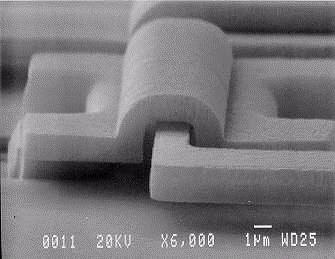
7 Hinges For 3D MEMS MEMS fabricated with conventional micromachining processes are essentially 2D (or 2½D ) Access to 3rd dimension with fold-up structures [Pister et al.1992] Are multi-link hinged structures possible in MUMPs? Figures: Kovacs 1998 Assembly/Deployment Of MEMS One-Time Deployment Of 3D Structures Manual assembly (tweezer, probe station, microscope) Agitation in fluid [Pister et al. 1992] Deployment actuators (Sandia) Assembly mechanism [Hui et al. 2000] Self-assembly inspired by chemistry and biology Sandia National Labs Hui et al. MEMS 2000
 A similar CCR structure in partially assembled state.")
8 MEMS Pop-Up Structures A) Unassembled pop-up cornercube reflector. B) CCR after assembly. The assembly was accomplished in a single flipping step. C) A similar CCR structure in partially assembled state. Designed in Sandia SUMMiT 4-level process by Elliot Hui, UC Berkeley Other Processes And Foundries CMOS Foundry Processes NMOS, PMOS and CMOS MOSIS Orbit 2.0 µm MEMS in CMOS CMOS MEMS Devices Bridges and cantilevers Hinges Multi-axis accelerometer
9 CMOS MEMS CMOS (complementary metal oxide semiconductor): the standard technology to build integrated circuits (ICs) Reasons for using CMOS for MEMS: Widely available foundry processes Well established and characterized Get integrated electronics for free (compare with MEMS pre or post processing) NMOS n-channel Metal Oxide Semiconductor Lilienfield, 1927, first transistor switch; US Patents 1,745,175 and 1,900,018. Bardeen, Brattain and Shockley, 1947, first bipolar transistor; Nobel Prize in Physics, n +5V Positive charge on gate creates n-type channel in p-doped substrate (Field Effect Transistor, FET) n p Comparison: capacitor G S D Switch 0V 5V
10 NMOS Fabrication p Grow 4000Å oxide on p-type silicon substrate As p p Pattern and etch oxide, then ion implant As to form n region Grow thin oxide (200Å), pattern and etch oxide to form contact Deposit 5000Å aluminum, pattern and etch aluminum Si SiO 2 n-si Al p NMOS capacitor NMOS Components Source Gate Drain p NMOS transistor Si SiO 2 n-si Al PSG
11 PMOS p-channel Metal Oxide Semiconductor p p V n Negative charge on gate creates p-type channel in n-doped substrate S G D Switch Comparison: capacitor 0V 5V CMOS Complementary Metal Oxide Semiconductor NMOS PMOS +5V Uses both NMOS and PMOS transistors Minimize power: high current only briefly during switching V out I PMOS NMOS V in +5V V in V out
12 CMOS V out Inverter NMOS PMOS +5V V out V in V in I PMOS NMOS +5V V out V in CMOS Inverter V in V out +5V n n p p p-well n-substrate Fabrication similar to PMOS, but we need additional pwell (= p-tub ) in n-type substrate (or vice versa) Doping of p-well overcompensates n-type doping of substrate Twin well process is also possible
13 CMOS Fabrication (simplified) / NWEL ion implant P Grow 100Å pad oxide Deposit 1000Å nitride / ACTV Grow 0.6 µm field oxide Strip nitride / pad oxide Grow 400Å gate oxide Deposit 0.4 µm n+poly / POLY / PSEL ion implant B, anneal (self-aligning) note: anneal not possible with Al pad / NSEL ion implant P, anneal CMOS Fabrication (simplified) Deposit 0.5µm LPCVD oxide, reflow / CONT Sputter Al + 2% Si / MET1 Ground V out +5V Deposit 0.6µm LPCVD oxide / VIA1 Sputter Al + 2% Si / MET2 Repeat oxide / Al as desired Deposit overglass 1µm / OG protective layer / holes for bonding pads
14 Mask Layers: CMOS Design NWEL defines n-well in p-type substrate ACTV active region (substrate exposed) POLY polysilicon (gates) PSEL p-type areas (in n-well) NSEL n-type areas CONT CMOS contacts MET1 metal layer 1 VIA1 via metal 1 - metal 2 MET2 metal layer 2 OG bonding pads CAD Convention: Draw conductors (Al, poly) CMOS CAD Example 1: Don t draw anything End up with Si, field oxide, Draw holes in dielectrics oxide 1, oxide 2, overglass (oxide, nitride, OG) Example 2: Draw all contacts (ACTV, CONT, VIA, OG) End up with bare Si (metal etch chews into Si) unpredictable
15 CMOS Example MET1 MET2 MET1, MET2 PIT (ACTV, CONT, VIA, OG) Design Rules (2µm Orbit) LayerLine / Space NWEL 10 / 9 ACTV 3 / 3 POLY 2 / 2 MET1 3 /3 MET2 3 / 4 OG 20 / 20 PIT 20 / 20 CONT - VIA (MET1 - POLY, MET1 - ACTV, MET1- MET2) 2 x 2 (2 µm space) Conductor Overlap 2 µm tolerance
16 2 µm Orbit Specifications 2 µm Orbit Specifications
17 CMOS Al Microhinge Hoffman, Warneke, Kruglick, Weigold and Pister (MEMS 1995) use CMOS field oxide as sacrificial layer BOE release etch Al provides mechanical and electrical connection for hinged structures Si SiO 2 Poly Al CMOS Al Microhinge Hoffman, Warneke, Kruglick, Weigold and Pister (MEMS 1995) XeF 2 bulk isotropic Si release etch Can vary stiffness of hinges and released structures Si SiO 2 Poly Al
 use CMOS field oxide as sacrificial layer Also: - Expose")

 Warneke et al. 1995 (UCLA) Storment et al.")
18 CMOS Microbridge Parameswaran, Baltes, Ristic, Dhaded and Robinson (Sensors and Actuators, 19, 1989) use CMOS field oxide as sacrificial layer Also: - Expose silicon substrate - Etch stop with heavily doped source/drain Si Si SiO 2 Poly Al Review Of XeF 2 Isotropic Silicon Etch Post-processing for standard CMOS Suspended and 3D structures Fold-up structures with conducting Al hinges Tahhan et al (UC Berkeley) Warneke et al (UCLA) Storment et al (Stanford)


19 3-Axis CMOS Accelerometer Regular 2 µm CMOS foundry process Single maskless post-processing step Kruglick, Warneke and Pister, MEMS, Accelerometer With CMOS/DRIE X. Zhu,D. W. Greve, G. K. Fedder, Characterization of Silicon Isotropic Etch by Inductively Coupled Plasma Etch in Post-CMOS Processing, IEEE MEMS 2000, Myazaki, Japan.
 - Lithography, Electroplating, Molding Invented in the")
, Karlsuhe, Germany Figure: G. Kovacs 1996")
20 Fundamental MEMS Processes And Devices High Aspect-Ratio Micro Structures (HARMST) LIGA SU-8 The LIGA Process LIGA stands for Lithographie, Galvanoformung, Abformung (german) - Lithography, Electroplating, Molding Invented in the late 70 s at the Nuclear Research Center, Karlsruhe, Germany Very high-aspect ratio microstructures achieved with X-ray lithography Figure: Institute for Microstructure Technology (FZK), Karlsuhe, Germany Figure: G. Kovacs 1996

21 LIGA Process Sequence Figure: W. Menz, J. Mohr and O. Paul, 2001, p LIGA Process (a) Plastic (usually PMMA, polymethyl methacrylate) on conductive substrate; several 100 µm thick. Exposure with very parallel X-rays (λ = nm) and development (b) Electroplating and removal of remaining PMMA (Cu, Ni, Au, ) (c) Injection molding in metal master (mass production) (d) Further processing (additional electroplating, )
 LIGA Mask Making Intermediate Mask Final Mask Intermediate mask required to make final mask Figure: W. Menz, J. Mohr, O. Paul, 2001, p.")
22 LIGA Mask: LIGA Mask Making Absorber (for X-rays): Au (> 10 µm) Carrier foil (transmission of X-rays, structural support of mask features): low absorbance and high resistance to X-rays required: Be, C, S, Frame (typical: 25 mm x 65 mm) LIGA Mask Making Intermediate Mask Final Mask Intermediate mask required to make final mask Figure: W. Menz, J. Mohr, O. Paul, 2001, p. 294.

23 X-Ray Lithography Issues Source: synchrotron Resist sensitive to X-rays Irradiation breaks up polymer chains Developer / solvent for breakup products Figure: W. Menz, J. Mohr and O. Paul 2001, p Electroplating In LIGA PMMA structures made in LIGA can be the end product Or, they can be a template for an electroplating process That process, in turn, can produce the master for a molding process Those molds, in turn, can be used in other production processes Figure: W. Menz, J. Mohr and O. Paul 2001, p. 320.

 High start-up costs Figure: W.")
24 Mold Template Fabrication Electroplating over PMMA structures Continues beyond height of PMMA structures to form continuous metal plate Polishing Figure: W. Menz, J. Mohr and O. Paul 2001, p Advantages Of LIGA Very high-aspect ratios Smooth sidewalls (compare to DRIE) Mass production by molding Disadvantages: Synchrotron required Material selection limited Complex processing steps (see, e.g., mask making) High start-up costs Figure: W. Menz, J. Mohr and O. Paul 2001, p. 310.

25 Applications Electrostatic comb drive Microturbines and flow sensors Figures: W. Menz, J. Mohr and O. Paul, 2001, p Applications Electromagnetic Actuator
26 LIGA Lithographie, Galvanoformung, Abformung (German: Lithography, Electroplating, Molding) Very high-aspect ratio micro molds Figure: G. Kovacs 1996 Alternatives To LIGA DRIE (deep reactive ion etching in Si): now widely used in academia and industry sidewalls not smooth ( scallops ) SU-8 ( poor man s LIGA )
27 SU-8 Thick Photoresists Negative UV Photoresist Up to 1200µm thickness (> 300 µm single spin) Aspect ratios up to 20:1 Processing with regular lithography equipment Features: Fast prototyping Durable structural material (epoxy) Adhesion to substrate materials? High stresses in SU-8 layers Low cost SU-8 Thick Photoresist Composition: Organic solvent GBL (gamma-butyloracton), determines viscosity and, thus, film thickness Epoxy resin (EPON resin SU-8) Photoinitiator Exposed SU-8 polymerizes and forms very durable structures Chemical amplification: chain reaction during exposure helps formation of vertical sidewalls


 X-ray detector (Brookhaven")
28 Thick-Film Photoresists Recently, results similar to LIGA have been achieved with SU-8, a negative photoresist for UV optical lithography Single and multi level structures: low cost molded watch gears (EPFL Switzerland 1997) X-ray detector (Brookhaven National Labs 1998)
4/10/2012. Introduction to Microfabrication. Fabrication
 Introduction to Microfabrication Fabrication 1 MEMS Fabrication Flow Basic Process Flow in Micromachining Nadim Maluf, An introduction to Microelectromechanical Systems Engineering 2 Thin Film Deposition
Lecture 10: MultiUser MEMS Process (MUMPS)
") MEMS: Fabrication Lecture 10: MultiUser MEMS Process (MUMPS) Prasanna S. Gandhi Assistant Professor, Department of Mechanical Engineering, Indian Institute of Technology, Bombay, 1 Recap Various VLSI based
MEMS: Fabrication Lecture 10: MultiUser MEMS Process (MUMPS) Prasanna S. Gandhi Assistant Professor, Department of Mechanical Engineering, Indian Institute of Technology, Bombay, 1 Recap Various VLSI based
Surface micromachining and Process flow part 1
 Surface micromachining and Process flow part 1 Identify the basic steps of a generic surface micromachining process Identify the critical requirements needed to create a MEMS using surface micromachining
Process Integration. NMOS Generic NMOS Process Flow. CMOS - The MOSIS Process Flow
 Process Integration Self-aligned Techniques LOCOS- self-aligned channel stop Self-aligned Source/Drain Lightly Doped Drain (LDD) Self-aligned silicide (SALICIDE) Self-aligned oxide gap MEMS Release Techniques
Lecture 7 CMOS MEMS. CMOS MEMS Processes. CMOS MEMS Processes. Why CMOS-MEMS? Agenda: CMOS MEMS: Fabrication. MEMS structures can be made
 EEL6935 Advanced MEMS (Spring 2005) Instructor: Dr. Huikai Xie CMOS MEMS Agenda: Lecture 7 CMOS MEMS: Fabrication Pre-CMOS Intra-CMOS Post-CMOS Deposition Etching Why CMOS-MEMS? Smart on-chip CMOS circuitry
ME 189 Microsystems Design and Manufacture. Chapter 9. Micromanufacturing
 ME 189 Microsystems Design and Manufacture Chapter 9 Micromanufacturing This chapter will offer an overview of the application of the various fabrication techniques described in Chapter 8 in the manufacturing
6.777J/2.732J Design and Fabrication of Microelectromechanical Devices Spring Term Solution to Problem Set 2 (16 pts)
") 6.777J/2.732J Design and Fabrication of Microelectromechanical Devices Spring Term 2007 By Brian Taff (Adapted from work by Feras Eid) Solution to Problem Set 2 (16 pts) Issued: Lecture 4 Due: Lecture
6.777J/2.732J Design and Fabrication of Microelectromechanical Devices Spring Term 2007 By Brian Taff (Adapted from work by Feras Eid) Solution to Problem Set 2 (16 pts) Issued: Lecture 4 Due: Lecture
EE C245 ME C218 Introduction to MEMS Design Fall 2011
 Lecture Outline EE C245 ME C218 Introduction to MEMS Design Fall 2011 Prof. Clark T.-C. Nguyen Dept. of Electrical Engineering & Computer Sciences University of California at Berkeley Berkeley, CA 94720
Surface Micromachining
 Surface Micromachining Outline Introduction Material often used in surface micromachining Material selection criteria in surface micromachining Case study: Fabrication of electrostatic motor Major issues
Lecture 030 Integrated Circuit Technology - I (5/8/03) Page 030-1
 Page 030-1") Lecture 030 Integrated Circuit Technology - I (5/8/03) Page 030-1 LECTURE 030 INTEGRATED CIRCUIT TECHNOLOGY - I (References [7,8]) Objective The objective of this presentation is: 1.) Illustrate integrated
Lecture 030 Integrated Circuit Technology - I (5/8/03) Page 030-1 LECTURE 030 INTEGRATED CIRCUIT TECHNOLOGY - I (References [7,8]) Objective The objective of this presentation is: 1.) Illustrate integrated
VLSI INTRODUCTION P.VIDYA SAGAR ( ASSOCIATE PROFESSOR) Department of Electronics and Communication Engineering, VBIT
 Department of Electronics and Communication Engineering, VBIT") VLSI INTRODUCTION P.VIDYA SAGAR ( ASSOCIATE PROFESSOR) contents UNIT I INTRODUCTION: Introduction to IC Technology MOS, PMOS, NMOS, CMOS & BiCMOS technologies. BASIC ELECTRICAL PROPERTIES : Basic Electrical
VLSI INTRODUCTION P.VIDYA SAGAR ( ASSOCIATE PROFESSOR) contents UNIT I INTRODUCTION: Introduction to IC Technology MOS, PMOS, NMOS, CMOS & BiCMOS technologies. BASIC ELECTRICAL PROPERTIES : Basic Electrical
3.155J / 6.152J Micro/Nano Processing Technology TAKE-HOME QUIZ FALL TERM 2005
 3.155J / 6.152J Micro/Nano Processing Technology TAKE-HOME QUIZ FALL TERM 2005 1) This is an open book, take-home quiz. You are not to consult with other class members or anyone else. You may discuss the
Fabrication and Layout
 Fabrication and Layout Kenneth Yun UC San Diego Adapted from EE271 notes, Stanford University Overview Semiconductor properties How chips are made Design rules for layout Reading Fabrication: W&E 3.1,
Lecture 5. SOI Micromachining. SOI MUMPs. SOI Micromachining. Silicon-on-Insulator Microstructures. Agenda:
 EEL6935 Advanced MEMS (Spring 2005) Instructor: Dr. Huikai Xie SOI Micromachining Agenda: SOI Micromachining SOI MUMPs Multi-level structures Lecture 5 Silicon-on-Insulator Microstructures Single-crystal
Lecture 19 Microfabrication 4/1/03 Prof. Andy Neureuther
 EECS 40 Spring 2003 Lecture 19 Microfabrication 4/1/03 Prof. ndy Neureuther How are Integrated Circuits made? Silicon wafers Oxide formation by growth or deposition Other films Pattern transfer by lithography
FABRICATION of MOSFETs
 FABRICATION of MOSFETs CMOS fabrication sequence -p-type silicon substrate wafer -creation of n-well regions for pmos transistors, -impurity implantation into the substrate. -thick oxide is grown in the
EECS130 Integrated Circuit Devices
 EECS130 Integrated Circuit Devices Professor Ali Javey 9/13/2007 Fabrication Technology Lecture 1 Silicon Device Fabrication Technology Over 10 15 transistors (or 100,000 for every person in the world)
Chapter 3 Silicon Device Fabrication Technology
 Chapter 3 Silicon Device Fabrication Technology Over 10 15 transistors (or 100,000 for every person in the world) are manufactured every year. VLSI (Very Large Scale Integration) ULSI (Ultra Large Scale
SURFACE MICROMACHINING
 SURFACE MICROMACHINING Features are built up, layer by layer on the surface of a substrate. Surface micromachined devices are much smaller than bulk micromachined components. Nature of deposition process
CMOS FABRICATION. n WELL PROCESS
 CMOS FABRICATION n WELL PROCESS Step 1: Si Substrate Start with p- type substrate p substrate Step 2: Oxidation Exposing to high-purity oxygen and hydrogen at approx. 1000 o C in oxidation furnace SiO
Isolation Technology. Dr. Lynn Fuller
 ROCHESTER INSTITUTE OF TECHNOLOGY MICROELECTRONIC ENGINEERING Isolation Technology Dr. Lynn Fuller Motorola Professor 82 Lomb Memorial Drive Rochester, NY 14623-5604 Tel (585) 475-2035 Fax (585) 475-5041
Fabrication and Layout
 ECEN454 Digital Integrated Circuit Design Fabrication and Layout ECEN 454 3.1 A Glimpse at MOS Device Polysilicon Aluminum ECEN 475 4.2 1 Material Classification Insulators Glass, diamond, silicon oxide
Micro-Electro-Mechanical Systems (MEMS) Fabrication. Special Process Modules for MEMS. Principle of Sensing and Actuation
 Fabrication. Special Process Modules for MEMS. Principle of Sensing and Actuation") Micro-Electro-Mechanical Systems (MEMS) Fabrication Fabrication Considerations Stress-Strain, Thin-film Stress, Stiction Special Process Modules for MEMS Bonding, Cavity Sealing, Deep RIE, Spatial forming
Micro-Electro-Mechanical Systems (MEMS) Fabrication Fabrication Considerations Stress-Strain, Thin-film Stress, Stiction Special Process Modules for MEMS Bonding, Cavity Sealing, Deep RIE, Spatial forming
Micro-Scale Engineering I Microelectromechanical Systems (MEMS) Y. C. Lee
 Y. C. Lee") Micro-Scale Engineering I Microelectromechanical Systems (MEMS) Y. C. Lee Department of Mechanical Engineering University of Colorado Boulder, CO 80309-0427 leeyc@colorado.edu September 2, 2008 1 Three
Micro-Scale Engineering I Microelectromechanical Systems (MEMS) Y. C. Lee Department of Mechanical Engineering University of Colorado Boulder, CO 80309-0427 leeyc@colorado.edu September 2, 2008 1 Three
VLSI Systems and Computer Architecture Lab
 ΚΥΚΛΩΜΑΤΑ VLSI Πανεπιστήμιο Ιωαννίνων CMOS Technology Τμήμα Μηχανικών Η/Υ και Πληροφορικής 1 From the book: An Introduction ti to VLSI Process By: W. Maly ΚΥΚΛΩΜΑΤΑ VLSI Διάρθρωση 1. N well CMOS 2. Active
EE40 Lec 22. IC Fabrication Technology. Prof. Nathan Cheung 11/19/2009
 Suggested Reading EE40 Lec 22 IC Fabrication Technology Prof. Nathan Cheung 11/19/2009 300mm Fab Tour http://www-03.ibm.com/technology/manufacturing/technology_tour_300mm_foundry.html Overview of IC Technology
EEC 118 Lecture #5: MOS Fabrication. Rajeevan Amirtharajah University of California, Davis Jeff Parkhurst Intel Corporation
 EEC 118 Lecture #5: MOS Fabrication Rajeevan Amirtharajah University of California, Davis Jeff Parkhurst Intel Corporation Announcements Lab 3 this week, report due next week HW 3 due this Friday at 4
EE 560 FABRICATION OF MOS CIRCUITS. Kenneth R. Laker, University of Pennsylvania
 1 EE 560 FABRICATION OF MOS CIRCUITS 2 CMOS CHIP MANUFACTRING STEPS Substrate Wafer Wafer Fabrication (diffusion, oxidation, photomasking, ion implantation, thin film deposition, etc.) Finished Wafer Wafer
Lecture 6. Through-Wafer Interconnect. Agenda: Through-wafer Interconnect Polymer MEMS. Through-Wafer Interconnect -1. Through-Wafer Interconnect -2
 Agenda: EEL6935 Advanced MEMS (Spring 2005) Instructor: Dr. Huikai Xie Lecture 6 Through-wafer Interconnect EEL6935 Advanced MEMS 2005 H. Xie 1/21/2005 1 Motivations: Wafer-level packaging CMOS 3D Integration
CMOS Manufacturing process. Circuit designer. Design rule set. Process engineer. Set of optical masks. Fabrication process.
 CMOS Manufacturing process Circuit design Set of optical masks Fabrication process Circuit designer Design rule set Process engineer All material: Chap. 2 of J. Rabaey, A. Chandrakasan, B. Nikolic, Digital
FABRICATION PROCESSES FOR MAGNETIC MICROACTUATORS WITH POLYSILICON FLEXURES. Jack W. Judy and Richard S. Muller
 FABRICATION PROCESSES FOR MAGNETIC MICROACTUATORS WITH POLYSILICON FLEXURES Jack W. Judy and Richard S. Muller Berkeley Sensor & Actuator Center (BSAC) Department of EECS, University of California, Berkeley,
Introduction to Micro/Nano Fabrication Techniques. Date: 2015/05/22 Dr. Yi-Chung Tung. Fabrication of Nanomaterials
 Introduction to Micro/Nano Fabrication Techniques Date: 2015/05/22 Dr. Yi-Chung Tung Fabrication of Nanomaterials Top-Down Approach Begin with bulk materials that are reduced into nanoscale materials Ex:
Lecture 22: Integrated circuit fabrication
 Lecture 22: Integrated circuit fabrication Contents 1 Introduction 1 2 Layering 4 3 Patterning 7 4 Doping 8 4.1 Thermal diffusion......................... 10 4.2 Ion implantation.........................
ELEC 3908, Physical Electronics, Lecture 4. Basic Integrated Circuit Processing
 ELEC 3908, Physical Electronics, Lecture 4 Basic Integrated Circuit Processing Lecture Outline Details of the physical structure of devices will be very important in developing models for electrical behavior
VLSI Technology. By: Ajay Kumar Gautam
 By: Ajay Kumar Gautam Introduction to VLSI Technology, Crystal Growth, Oxidation, Epitaxial Process, Diffusion Process, Ion Implantation, Lithography, Etching, Metallization, VLSI Process Integration,
CTN 10/1/09. EE 245: Introduction to MEMS Lecture 11: Bulk Micromachining. Copyright 2009 Regents of the University of California
 MUMPS: MultiUser MEMS ProcesS Foundry MEMS: The MUMPS Process Originally created by the Microelectronics Center of North Carolina (MCNC) now owned by MEMSCAP in France Three-level polysilicon surface micromachining
3. Overview of Microfabrication Techniques
 3. Overview of Microfabrication Techniques The Si revolution First Transistor Bell Labs (1947) Si integrated circuits Texas Instruments (~1960) Modern ICs More? Check out: http://www.pbs.org/transistor/background1/events/miraclemo.html
Applications of High-Performance MEMS Pressure Sensors Based on Dissolved Wafer Process
 Applications of High-Performance MEMS Pressure Sensors Based on Dissolved Wafer Process Srinivas Tadigadapa and Sonbol Massoud-Ansari Integrated Sensing Systems (ISSYS) Inc., 387 Airport Industrial Drive,
Integrated Processes. Lecture Outline
 Integrated Processes Thara Srinivasan Lecture 14 Picture credit: Lemkin et al. Lecture Outline From reader Bustillo, J. et al., Surface micromachining of MEMS, pp. 1556-9. A.E. Franke et al., Polycrystalline
Regents of the University of California
 Surface-Micromachining Process Flow Photoresist Sacrificial Oxide Structural Polysilcon Deposit sacrificial PSG: Target = 2 m 1 hr. 40 min. LPCVD @450 o C Densify the PSG Anneal @950 o C for 30 min. Lithography
CMOS Manufacturing Process
 CMOS Manufacturing Process CMOS Process A Modern CMOS Process gate-oxide TiSi 2 AlCu Tungsten SiO 2 n+ p-well p-epi poly n-well p+ SiO 2 p+ Dual-Well Trench-Isolated CMOS Process Circuit Under Design V
EE 330 Lecture 9. IC Fabrication Technology Part II. -Oxidation -Epitaxy -Polysilicon -Planarization -Resistance and Capacitance in Interconnects
 EE 330 Lecture 9 IC Fabrication Technology Part II -Oxidation -Epitaxy -Polysilicon -Planarization -Resistance and Capacitance in Interconnects Review from Last Time Etching Dry etch (anisotropic) SiO
EE 434 Lecture 9. IC Fabrication Technology
 EE 434 Lecture 9 IC Fabrication Technology Quiz 7 The layout of a film resistor with electrodes A and B is shown. If the sheet resistance of the film is 40 /, determine the resistance between nodes A and
Manufacturing Process
 Digital Integrated Circuits A Design Perspective Jan M. Rabaey Anantha Chandrakasan Borivoje Nikolic Manufacturing Process July 30, 2002 1 CMOS Process 2 A Modern CMOS Process gate-oxide TiSi 2 AlCu Tungsten
Uncrosslinked SU-8 as a sacrificial material
 INSTITUTE OFPHYSICS PUBLISHING JOURNAL OF MICROMECHANICS AND MICROENGINEERING J. Micromech. Microeng. 15 (2005) N1 N5 doi:10.1088/0960-1317/15/1/n01 TECHNICAL NOTE Uncrosslinked as a sacrificial material
Ajay Kumar Gautam [VLSI TECHNOLOGY] VLSI Technology for 3RD Year ECE/EEE Uttarakhand Technical University
![Ajay Kumar Gautam [VLSI TECHNOLOGY] VLSI Technology for 3RD Year ECE/EEE Uttarakhand Technical University](/thumbs/75/72824557.jpg "Ajay Kumar Gautam [VLSI TECHNOLOGY] VLSI Technology for 3RD Year ECE/EEE Uttarakhand Technical University") 2014 Ajay Kumar Gautam [VLSI TECHNOLOGY] VLSI Technology for 3RD Year ECE/EEE Uttarakhand Technical University Page1 Syllabus UNIT 1 Introduction to VLSI Technology: Classification of ICs, Scale of integration,
2014 Ajay Kumar Gautam [VLSI TECHNOLOGY] VLSI Technology for 3RD Year ECE/EEE Uttarakhand Technical University Page1 Syllabus UNIT 1 Introduction to VLSI Technology: Classification of ICs, Scale of integration,
Lecture 200 BiCMOS Technology (12/12/01) Page 200-1
 Page 200-1") Lecture 200 BiCMOS Technology (12/12/01) Page 200-1 LECTURE 200 BICMOS TECHNOLOGY (READING: Text-Sec. 2.11) INTRODUCTION Objective Illustrate BiCMOS technology Outline Introduction Physical process illustration
Lecture 200 BiCMOS Technology (12/12/01) Page 200-1 LECTURE 200 BICMOS TECHNOLOGY (READING: Text-Sec. 2.11) INTRODUCTION Objective Illustrate BiCMOS technology Outline Introduction Physical process illustration
Gaetano L Episcopo. Introduction to MEMS
 Gaetano L Episcopo Introduction to MEMS What are MEMS? Micro Electro Mechanichal Systems MEMS are integrated devices, or systems of devices, with microscopic parts, such as: Mechanical Parts Electrical
MEMS Fabrication I : Process Flows and Bulk Micromachining
 MEMS Fabrication I : Process Flows and Bulk Micromachining Dr. Thara Srinivasan Lecture 2 Picture credit: Alien Technology Lecture Outline Reading Reader is in! (at South side Copy Central) Kovacs, Bulk
FABRICATION ENGINEERING MICRO- NANOSCALE ATTHE AND. Fourth Edition STEPHEN A. CAMPBELL. of Minnesota. University OXFORD UNIVERSITY PRESS
 AND FABRICATION ENGINEERING ATTHE MICRO- NANOSCALE Fourth Edition STEPHEN A. CAMPBELL University of Minnesota New York Oxford OXFORD UNIVERSITY PRESS CONTENTS Preface xiii prrt i OVERVIEW AND MATERIALS
Surface Micromachining II
 Surface Micromachining II Dr. Thara Srinivasan Lecture 4 Picture credit: Sandia National Lab Lecture Outline Reading From reader: Bustillo, J. et al., Surface Micromachining of Microelectromechanical Systems,
Lecture 2. Fabrication and Layout
 Lecture 2 Fabrication and Layout Mark Horowitz Modified by Azita Emami Computer Systems Laboratory Stanford University azita@stanford.edu 1 Overview Reading W&E 3.1(scan), 3.2.1, 3.3.1 - Fabrication W&E
Atomic Layer Deposition(ALD)
") Atomic Layer Deposition(ALD) AlO x for diffusion barriers OLED displays http://en.wikipedia.org/wiki/atomic_layer_deposition#/media/file:ald_schematics.jpg Lam s market-leading ALTUS systems combine CVD
Atomic Layer Deposition(ALD) AlO x for diffusion barriers OLED displays http://en.wikipedia.org/wiki/atomic_layer_deposition#/media/file:ald_schematics.jpg Lam s market-leading ALTUS systems combine CVD
SOIMUMPs Design Handbook
 SOIMUMPs Design Handbook a MUMPs process C. J. Han, Allen Cowen, Greg Hames and Busbee Hardy MEMScAP Revision 3.0 Copyright 2002 by MEMScAP. All rights reserved. Permission to use and copy for internal,
National Semiconductor LM2672 Simple Switcher Voltage Regulator
 Construction Analysis National Semiconductor LM2672 Simple Switcher Voltage Regulator Report Number: SCA 9712-570 Global Semiconductor Industry the Serving Since 1964 17350 N. Hartford Drive Scottsdale,
Historical Development. Babbage s second computer. Before the digital age
 Historical Development To fully appreciate the computers of today, it is helpful to understand how things got the way they are The evolution of computing machinery has taken place over several centuries
Cristina Rusu Imego AB Cristina Rusu
 MEMS Fabrication Cristina Rusu Imego AB 2011-02-21 MEMS Semiconductors as mechanical materials Bulk micromachining Dry etching Wet etching Surface micromachining MUMPs Polymer MEMS Wafer bonding Technology:
Semiconductor Manufacturing Technology. IC Fabrication Process Overview
 Semiconductor Manufacturing Technology Michael Quirk & Julian Serda October 00 by Prentice Hall Chapter 9 IC Fabrication Process Overview /4 Objectives After studying the material in this chapter, you
Dallas Semicoductor DS80C320 Microcontroller
 Construction Analysis Dallas Semicoductor DS80C320 Microcontroller Report Number: SCA 9702-525 Global Semiconductor Industry the Serving Since 1964 15022 N. 75th Street Scottsdale, AZ 85260-2476 Phone:
Silicon Manufacturing
 Silicon Manufacturing Group Members Young Soon Song Nghia Nguyen Kei Wong Eyad Fanous Hanna Kim Steven Hsu th Fundamental Processing Steps 1.Silicon Manufacturing a) Czochralski method. b) Wafer Manufacturing
Silicon Wafer Processing PAKAGING AND TEST
 Silicon Wafer Processing PAKAGING AND TEST Parametrical test using test structures regularly distributed in the wafer Wafer die test marking defective dies dies separation die fixing (not marked as defective)
Plasma Etching Rates & Gases Gas ratios affects etch rate & etch ratios to resist/substrate
 Plasma Etching Rates & Gases Gas ratios affects etch rate & etch ratios to resist/substrate Development of Sidewalls Passivating Films Sidewalls get inert species deposited on them with plasma etch Creates
Cost of Integrated Circuits
 Cost of IC Design 1 Cost of Integrated Circuits NRE (Non-Recurrent Engineering) costs fixed design time and effort, mask generation independent of sales volume / number of products one-time cost factor
SUMMiT V Five Level Surface Micromachining Technology Design Manual
 SUMMiT V Five Level Surface Micromachining Technology Design Manual Version 1.3 09/22/2005 MEMS Devices and Reliability Physics Department Microelectronics Development Laboratory Sandia National Laboratories
KGC SCIENTIFIC Making of a Chip
 KGC SCIENTIFIC www.kgcscientific.com Making of a Chip FROM THE SAND TO THE PACKAGE, A DIAGRAM TO UNDERSTAND HOW CPU IS MADE? Sand CPU CHAIN ANALYSIS OF SEMICONDUCTOR Material for manufacturing process
Proceedings Post Fabrication Processing of Foundry MEMS Structures Exhibiting Large, Out-of-Plane Deflections
 Proceedings Post Fabrication Processing of Foundry MEMS Structures Exhibiting Large, Out-of-Plane Deflections LaVern Starman 1, *, John Walton 1, Harris Hall 1 and Robert Lake 2 1 Sensors Directorate,
Process Flow in Cross Sections
 Process Flow in Cross Sections Process (simplified) 0. Clean wafer in nasty acids (HF, HNO 3, H 2 SO 4,...) --> wear gloves! 1. Grow 500 nm of SiO 2 (by putting the wafer in a furnace with O 2 2. Coat
ENG/PHYS3320 Microsystems Technology Chapter 2 Fabrication of Microsystems
 ENG/PHYS3320 Microsystems Technology Chapter 2 Fabrication of Microsystems ENG/PHYS3320: R.I. Hornsey Fab: 1 Fabrication Many of the new transducers are based on a technology known as micromachining a
Figure 2.3 (cont., p. 60) (e) Block diagram of Pentium 4 processor with 42 million transistors (2000). [Courtesy Intel Corporation.
 (e) Block diagram of Pentium 4 processor with 42 million transistors (2000). [Courtesy Intel Corporation.") Figure 2.1 (p. 58) Basic fabrication steps in the silicon planar process: (a) oxide formation, (b) selective oxide removal, (c) deposition of dopant atoms on wafer, (d) diffusion of dopant atoms into exposed
Figure 2.1 (p. 58) Basic fabrication steps in the silicon planar process: (a) oxide formation, (b) selective oxide removal, (c) deposition of dopant atoms on wafer, (d) diffusion of dopant atoms into exposed
Single crystal silicon supported thin film micromirrors for optical applications
 Single crystal silicon supported thin film micromirrors for optical applications Zhimin J. Yao* Noel C. MacDonald Cornell University School of Electrical Engineering and Cornell Nanofabrication Facility
Lab #2 Wafer Cleaning (RCA cleaning)
") Lab #2 Wafer Cleaning (RCA cleaning) RCA Cleaning System Used: Wet Bench 1, Bay1, Nanofabrication Center Chemicals Used: H 2 O : NH 4 OH : H 2 O 2 (5 : 1 : 1) H 2 O : HF (10 : 1) H 2 O : HCl : H 2 O 2
Lab #2 Wafer Cleaning (RCA cleaning) RCA Cleaning System Used: Wet Bench 1, Bay1, Nanofabrication Center Chemicals Used: H 2 O : NH 4 OH : H 2 O 2 (5 : 1 : 1) H 2 O : HF (10 : 1) H 2 O : HCl : H 2 O 2
Rockwell R RF to IF Down Converter
 Construction Analysis Rockwell R6732-13 RF to IF Down Converter Report Number: SCA 9709-552 Global Semiconductor Industry the Serving Since 1964 17350 N. Hartford Drive Scottsdale, AZ 85255 Phone: 602-515-9780
Sensors and Actuators Designed and Fabricated in a. Micro-Electro-Mechanical-Systems (MEMS) Course. Using Standard MEMS Processes
 Course. Using Standard MEMS Processes") Sensors and Actuators Designed and Fabricated in a Micro-Electro-Mechanical-Systems (MEMS) Course Using Standard MEMS Processes M.G. Guvench University of Southern Maine guvench@maine.edu Abstract Use
Sensors and Actuators Designed and Fabricated in a Micro-Electro-Mechanical-Systems (MEMS) Course Using Standard MEMS Processes M.G. Guvench University of Southern Maine guvench@maine.edu Abstract Use
EE C245 ME C218 Introduction to MEMS Design Fall 2010
 Lecture Outline EE C245 ME C218 Introduction to MEMS Design Fall 2010 Prof. Clark T.-C. Nguyen Dept. of Electrical Engineering & Computer Sciences University of California at Berkeley Berkeley, CA 94720
HOMEWORK 4 and 5. March 15, Homework is due on Monday March 30, 2009 in Class. Answer the following questions from the Course Textbook:
 HOMEWORK 4 and 5 March 15, 2009 Homework is due on Monday March 30, 2009 in Class. Chapter 7 Answer the following questions from the Course Textbook: 7.2, 7.3, 7.4, 7.5, 7.6*, 7.7, 7.9*, 7.10*, 7.16, 7.17*,
Materials for MEMS. Dr. Yael Hanein. 11 March 2004 Materials Applications Yael Hanein
 Materials for MEMS Dr. Yael Hanein Materials for MEMS MEMS (introduction) Materials used in MEMS Material properties Standard MEMS processes MEMS The world s smallest guitar is about 10 micrometers long
Etching Etching Definitions Isotropic Etching: same in all direction Anisotropic Etching: direction sensitive Selectivity: etch rate difference
 Etching Etching Definitions Isotropic Etching: same in all direction Anisotropic Etching: direction sensitive Selectivity: etch rate difference between 2 materials Need strong selectivity from masking
1 Thin-film applications to microelectronic technology
 1 Thin-film applications to microelectronic technology 1.1 Introduction Layered thin-film structures are used in microelectronic, opto-electronic, flat panel display, and electronic packaging technologies.
PROCESSING OF INTEGRATED CIRCUITS
 PROCESSING OF INTEGRATED CIRCUITS Overview of IC Processing (Part I) Silicon Processing Lithography Layer Processes Use in IC Fabrication (Part II) Integrating the Fabrication Steps IC Packaging (Part
Welcome to. Celebrating 30 years in Semiconductor and Sensor device manufacture!
 Welcome to Celebrating 30 years in Semiconductor and Sensor device manufacture! Sensor and Silicon Solutions Over 250 million die shipped per year Fab 3 Fab 1 Fab 2 Probe & Test Semefab Overview! Commercial
Interconnects OUTLINE
 Interconnects 1 Interconnects OUTLINE 1. Overview of Metallization 2. Introduction to Deposition Methods 3. Interconnect Technology 4. Contact Technology 5. Refractory Metals and their Silicides Reading:
micro resist technology
 Characteristics Processing guidelines Negative Tone Photoresist Series ma-n 1400 ma-n 1400 is a negative tone photoresist series designed for the use in microelectronics and microsystems. The resists are
MEMS prototyping using RF sputtered films
 Indian Journal of Pure & Applied Physics Vol. 45, April 2007, pp. 326-331 MEMS prototyping using RF sputtered films Sudhir Chandra, Vivekanand Bhatt, Ravindra Singh, Preeti Sharma & Prem Pal* Centre for
TSV Processing and Wafer Stacking. Kathy Cook and Maggie Zoberbier, 3D Business Development
 TSV Processing and Wafer Stacking Kathy Cook and Maggie Zoberbier, 3D Business Development Outline Why 3D Integration? TSV Process Variations Lithography Process Results Stacking Technology Wafer Bonding
Technology. Semiconductor Manufacturing. Hong Xiao INTRODUCTION TO SECOND EDITION SPIE PRESS
 INTRODUCTION TO Semiconductor Manufacturing Technology SECOND EDITION Hong Xiao TECHNISCHE INFORMATIONSBiBUOTHEK UNIVERSITATSBIBLIOTHEK HANNOVER SPIE PRESS Bellingham,Washington USA Contents Preface to
5.8 Diaphragm Uniaxial Optical Accelerometer
 5.8 Diaphragm Uniaxial Optical Accelerometer Optical accelerometers are based on the BESOI (Bond and Etch back Silicon On Insulator) wafers, supplied by Shin-Etsu with (100) orientation, 4 diameter and
Intel Pentium Processor W/MMX
 Construction Analysis Intel Pentium Processor W/MMX Report Number: SCA 9706-540 Global Semiconductor Industry the Serving Since 1964 15022 N. 75th Street Scottsdale, AZ 85260-2476 Phone: 602-998-9780 Fax:
INTEGRATED MEMS IN CONVENTIONAL CMOS
 INTEGRATED MEMS IN CONVENTIONAL CMOS GARY K. FEDDER Department of Electrical and Computer Engineering and The Robotics Institute Carnegie Mellon University Pittsburgh, PA, 15213-3890 E-mail: fedder@ece.cmu.edu
Semiconductor Physics Course Final Presentation CMOS Fabrication by Özgür Çobanoğlu (Turin, 2006)
") Semiconductor Physics Course Final Presentation CMOS Fabrication by Özgür Çobanoğlu (Turin, 2006) 1 Outline Sections and Contents of the Presentation What is MOS? How does MOS behave in low level? A useful
Semiconductor Physics Course Final Presentation CMOS Fabrication by Özgür Çobanoğlu (Turin, 2006) 1 Outline Sections and Contents of the Presentation What is MOS? How does MOS behave in low level? A useful
HYPRES. Hypres MCM Process Design Rules 04/12/2016
 HYPRES Hypres MCM Process Design Rules 04/12/2016 Direct all inquiries, questions, comments and suggestions concerning these design rules and/or HYPRES fabrication to: Daniel T. Yohannes Tel. (914) 592-1190
Applications of LIGA on Micro-punching Process for Metallic Materials
 Materials Science Forum Vols. 505-507 (2006) pp. 55-60 online at http://www.scientific.net (2006) Trans Tech Publications, Switzerland Applications of LIGA on Micro-punching Process for Metallic Materials
Design and fabrication of MEMS devices using the integration of MUMPs, trench-refilled molding, DRIE and bulk silicon etching processes
 TB, KR, JMM/184987, 3/12/2004 INSTITUTE OF PHYSICS PUBLISHING JOURNAL OF MICROMECHANICS AND MICROENGINEERING J. Micromech. Microeng. 15 (2005) 1 8 doi:10.1088/0960-1317/15/0/000 Design and fabrication
Basic&Laboratory& Materials&Science&and&Engineering& Micro&Electromechanical&Systems&& (MEMS)&
&") Basic&Laboratory& Materials&Science&and&Engineering& Micro&Electromechanical&Systems&& (MEMS)& M105& As of: 27.10.2011 1 Introduction... 2 2 Materials used in MEMS fabrication... 2 3 MEMS fabrication processes...
Basic&Laboratory& Materials&Science&and&Engineering& Micro&Electromechanical&Systems&& (MEMS)& M105& As of: 27.10.2011 1 Introduction... 2 2 Materials used in MEMS fabrication... 2 3 MEMS fabrication processes...
Today s agenda (19-JAN-2010)
") Today s agenda (19-JAN-2010) 1) Overview of Integrated Circuit technology 2) Managing Deadlines 3) A look @ Spring Schedule 4) Suggested milestones 5) Project concept presentations Action items from last
Today s agenda (19-JAN-2010) 1) Overview of Integrated Circuit technology 2) Managing Deadlines 3) A look @ Spring Schedule 4) Suggested milestones 5) Project concept presentations Action items from last
A modular process for integrating thick polysilicon MEMS devices with sub-micron CMOS
 A modular process for integrating thick polysilicon MEMS devices with sub-micron CMOS John Yasaitis a, Michael Judy a, Tim Brosnihan a, Peter Garone a, Nikolay Pokrovskiy a, Debbie Sniderman a,scottlimb
Is Now Part of To learn more about ON Semiconductor, please visit our website at
 Is Now Part of To learn more about ON Semiconductor, please visit our website at www.onsemi.com ON Semiconductor and the ON Semiconductor logo are trademarks of Semiconductor Components Industries, LLC
Microstructures using RF sputtered PSG film as a sacrificial layer in surface micromachining
 Sādhanā Vol. 34, Part 4, August 2009, pp. 557 562. Printed in India Microstructures using RF sputtered PSG film as a sacrificial layer in surface micromachining VIVEKANAND BHATT 1,, SUDHIR CHANDRA 1 and
CMOS-MEMS integration
 CMOS-MEMS integration Jan Erik Ramstad Institute for Informatics University of Oslo janera@fys.uio.no 27th March 2006 Contents 1 Essay background 1 2 Processes 1 2.1 CMOS-MEMS process steps.............
Hitachi A 64Mbit (8Mb x 8) Dynamic RAM
 Dynamic RAM") Construction Analysis Hitachi 5165805A 64Mbit (8Mb x 8) Dynamic RAM Report Number: SCA 9712-565 Global Semiconductor Industry the Serving Since 1964 17350 N. Hartford Drive Scottsdale, AZ 85255 Phone:
Construction Analysis Hitachi 5165805A 64Mbit (8Mb x 8) Dynamic RAM Report Number: SCA 9712-565 Global Semiconductor Industry the Serving Since 1964 17350 N. Hartford Drive Scottsdale, AZ 85255 Phone:
Bulk Silicon Micromachining
 Bulk Silicon Micromachining Micro Actuators, Sensors, Systems Group University of Illinois at Urbana-Champaign Outline Types of bulk micromachining silicon anisotropic etching crystal orientation isotropic