Dr. Lynn Fuller, Motorola Professor Steven Sudirgo, Graduate Student
|
|
|
- Roy Lawson
- 6 years ago
- Views:
Transcription
1 ROCHESTER INSTITUTE OF TECHNOLOGY MICROELECTRONIC ENGINEERING Bulk Micromachined Pressure Sensor Dr. Lynn Fuller, Motorola Professor Steven Sudirgo, Graduate Student 82 Lomb Memorial Drive Rochester, NY Tel (585) Fax (585) Page 1
2 OUTLINE Piezoresistive Pressure Sensor Resistor Layout Maskmaking Alignment Details Process Details Packaging Testing Approach Test Results Page 2

3 SINGLE CRYSTAL SILICON Thickness 10 µm Wafer Diameter 75 mm Page 3
4 DESIGN GUIDELINES Each student has 5mm x 5mm area Diaphragm size up to 3mm Three Layer Design Diaphragm (Green) Resistor (Red) Metal (Blue) Page 4
5 BACKSIDE ETCHED BULK MICROMACHINED POLYSILICON RESISTOR PRESSURE SENSOR Polysilicon Resistors Aluminum Metal Silicon Nitride Insulator Si 500 µm Silicon Diaphragm Silicon Nitride Etch Mask Page 5

6 FINITE ELEMENT ANALYSIS Points of Maximum Stress Page 6


7 ANSYS FINITE ELEMENT ANALYSIS Regular SiDiaphragm Corrugated Diaphragm Layer 2: 1.5mm x 1.5mm Polysilicon 1µm thick 2mm x 2mm diaphragm 30µm thick, 50 psi applied Rob Manley, 2005 Page 7

8 DIAPHRAGM DEFORMATION MOVIE 200µm Rob Manley, 2005 Page 8

9 DIAPHRAGM STRESS MOVIE Rob Manley, 2005 Page 9
10 RESISTOR LAYOUT R1 R3 R2 R4 Two resistors parallel to edge near region of maximum stress and two resistors perpendicular to the edge arranged in a full bridge ciruit. If all resistors are of equal value then Vout = Vo1-Vo2 = zero with no pressure applied. Page 10
11 +5 Volts Vo1 Bulk Micromachined Pressure Sensor CALCULATION OF EXPECTED OUTPUT VOLTAGE R1 R3 R2 R4 Gnd Vo2 The equation for stress at the center edge of a square diaphragm (S.K. Clark and K.Wise, 1979) Stress = 0.3 P(L/H) 2 where P is pressure, L is length of diaphragm edge, H is diaphragm thickness For a 3000µm opening on the back of the wafer the diaphragm edge length L is (500/Tan 53 ) = 2246 µm Page 11
12 CALCULATION OF EXPECTED OUTPUT VOLTAGE (Cont.) Stress = 0.3 P (L/H) 2 If we apply vacuum to the back of the wafer that is equivalent to and applied pressure of 14.7 psi or 103 N/m 2 P = 103 N/m 2 L= 2246 µm Stress = 2.49E8 N/m H= 25 µm 2 Hooke s Law: Stress = E Strain where E is Young s Modulus σ = E ε Young s Modulus ofr silicon is 1.9E11 N/m 2 Thus the strain = 1.31E-3 or.131% Page 12
13 CALCULATION OF EXPECTED OUTPUT VOLTAGE (Cont.) The sheet resistance (Rhos) from 4 point probe is 61 ohms/sq The resistance is R = Rhos L/W For a resistor R3 of L=350 µm and W=50 µm we find: R3 = 61 (350/50) = ohms R3 and R2 decrease as W increases due to the strain assume L is does not change, W becomes 50+50x0.131% W = µm R3 = Rhos L/W = 61 (350/ ) = ohms R1 and R4 increase as L increases due to the strain assume W does not change, L becomes x0.131% R1 = Rhos L /W = 61 ( /50) = ohms Page 13
14 CALCULATION OF EXPECTED OUTPUT VOLTAGE (Cont.) 5 Volts R1=427 R3=427 Vo1=2.5v Vo2=2.5v No stress Vo2-Vo1 = 0 R1=427.6 Vo1=2.4965v 5 Volts R3=426.4 Vo2=2.5035v R2=427 R4=427 R2=426.4 R4=427.6 Gnd With stress Vo2-Vo1 = 0.007v =7 mv Gnd Page 14
15 BUFFER / DIFFERENTIAL AMPLIFIER / FILTER Vsupply Rf R1 R3 - + Va Rin Rin - + Rf Vo R2 R4 Gnd Gnd - + Vb Electronics Off-Chip May not be needed Page 15
16 5 X 5 ARRAY FOR 25 STUDENT DESIGNS Each Design 5mmx5mm Page 16

17 26 STUDENT DESIGNS 2002 Page 17

18 12 STUDENT DESIGNS 2003 Page 18
19 4 WAFER AND ARRAY 3 LAYERS Diaphragm Resistor Metal 3x3 array of 25 Designs For a total of 225 Sensors Page 19
20 ORDER MASK 1x Mask with pattern repeated 3x3 array for total of 9 Mirror Layers 2 (red poly) and 3 (blue metal) Do not mirror Layer 1 (green-diaphram) No alignment marks (we will align to the pattern) Page 20

21 MASK Page 21


22 CMP BACKSIDE OF WAFERS Strassbaugh CMP Tool Page 22
23 CMP DETAILS Strassbaugh CMP Tool Slurry: Lavisil , with ph=12, 15 min per wafer Slurry drip rate: ~1 drop/second Down Pressure = 8 psi Quill Speed = 70 rpm Oscillation Speed = 6 per min Table Speed = 50 rpm (~10 Hz) The quality of this polish must be very good. If after polish you can not visually tell the front from the back then it is good. Otherwise the subsequent nitride coating will not be good enough to act as an etch mask to KOH Page 23
24 RCA CLEAN WAFERS APM H 2 O 4500ml NH 4 OH 300ml H 2 O 2 900ml 75 C, 10 min. DI water rinse, 5 min. DI water rinse, 5 min. HPM H 2 O 4500ml HCL-300ml H 2 O 2 900ml 75 C, 10 min. H HF sec. DI water rinse, 5 min. SPIN/RINSE DRY What does RCA stand for? ANSWER PLAY Page 24
 Flow = 60 sccm Ammonia (NH3) Flow = 150 sccm Rate = 60 Å/min +/- 10 Å/min Time ~25 min for 1500 Å Page")
25 DEPOSIT PROTECTIVE SILICON NITRIDE LAYER Silicon Nitride (Si3N4) (normal - stociometric): Temperature = C Ramp from (door to pump) Pressure = 375 mtorr 3SiH2Cl2 + 4NH3 = Si3N4 + 9H2 + 3Cl2 Dichlorosilane (SiH2Cl2) Flow = 60 sccm Ammonia (NH3) Flow = 150 sccm Rate = 60 Å/min +/- 10 Å/min Time ~25 min for 1500 Å Page 25

26 PICTURE OF WAFER AFTER NITRIDE DEPOSITION This nitride is about 3500 Å thick. A thinner layer may have less stress and be less sensitive to microcracks and pinholes. Nitride does not etch in KOH so even a very thin layer will mask. Try ~1500 Å Page 26
27 (REFLECTANCE SPECTROMETER) NANOSPEC THICKNESS MEASUREMENT INCIDENT WHITE LIGHT, THE INTENSITY OF THE REFLECTED LIGHT IS MEASURED VS WAVELENGTH 3000 Å OXIDE 7000 Å OXIDE MONOCHROMATOR & DETECTOR l l WHITE LIGHT SOURCE WAFER OPTICS Oxide on Silicon ,000 Å Nitride ,000 Neg Resist ,000 Poly on Ox ,000 Neg Resist on Ox Nitride on Oxide Thin Oxide Thin Nitride Polyimide ,000 Positive Resist ,000 Pos Resist on Ox ,000 4,000-30,000 Page 27

28 NANOSPEC FILM THICKNESS MEASUREMENT TOOL Page 28
29 OXIDE THICKNESS COLOR CHART Thickness Color Thickness Color 500 Tan 4900 Blue Blue 700 Brown 5000 Blue Green 1000 Dark Violet - Red Violet 5200 Green 1200 Royal Blue 5400 Yellow Green Blue 1500 Light Blue - Metallic Blue 5600 GreenYellow 1700 Metallic - very light Yellow Green 5700 Yellow -"Yellowish"(at times appears to be Lt gray or matell 2000 LIght Gold or Yellow - Slightly Metallic 5800 Light Orange or Yellow - Pink 2200 Gold with slight Yellow Orange 6000 Carnation Pink 2500 Orange - Melon 6300 Violet Red 2700 Red Violet 6800 "Bluish"(appears violet red, Blue Green, looks grayish) Blue 3000 Blue - Violet Blue 7200 Blue Green - Green 3100 Blue Blue 7700 "Yellowish" 3200 Blue - Blue Green 8000 Orange 3400 Light Green 8200 Salmon 3500 Green - Yellow Green 8500 Dull, LIght Red Violet 3600 Yellow Green 8600 Violet X other materials = X oxide 1.45/n 3700 Yellow 8700 Blue Violet other material 3900 Light Orange 8900 Blue Blue 4100 Carnation Pink 9200 Blue Green 4200 Violet Red 9500 Dull Yellow Green 4400 Red Violet 9700 Yellow - "Yellowish" 4600 Violet 9900 Orange 4700 Blue Violet Carnation Pink Nitride Rochester Institute Thickness of Technology = (Oxide Thickness)(Oxide Index/Nitride Index) Eg. Yellow Nitride Thickness = (2000)(1.46/2.00) = 1460 Page 29
30 1 st LAYER LITHOGRAPHY The objective is to protect the nitride using photoresist on one side of the wafer prior to etching the pattern for the diaphragm holes in the nitride on the back of the wafers. The plasma etch will only etch from one side so the nitride on the other side of the wafer will remain after the nitride etch for the diaphragm holes. Page 30
31 COAT AND DEVELOP TRACK DEHYDRATE BAKE 200 C, 120 sec. Optional COAT COAT HMDS Vapor Prime S-8 RESIST 4500 rpm, 60 sec. SOFT BAKE 90 C 60 sec. POST EXPOSURE BAKE 115 C, 60 sec. Optional DEVELOP DEVELOP DI Wet CD-26 Developer 50 sec., Puddle Rinse, Spin Dry HARD BAKE 125 C, 60 sec. Page 31


32 AUTOMATED COAT AND DEVELOP TRACK Page 32
33 EXPOSURE TOOLS The resist needs and exposure dose (E) of about 50 mj/cm2. The intensity (I) is measured and found to be ~5 mw/cm2 so using the equation E=It we find exposure time of 10 seconds. SEE contact printers with back side alignment Page 33

34 IMAGES AFTER LITHOGRAPHY Resist on Nitride Nitride Page 34
35 SILICON NITRIDE ETCH The objective is to plasma etch the nitride down to the bare silicon on the back of the wafer in the areas where the holes to form the diaphragm will be etched. Since we intend to etch almost all the way through the silicon wafer it is not critical to stop the etch exactly after etching through the nitride. Page 35
36 OPEN DIAPHRAGM ETCH HOLES Lam 490 Etch Tool Plasma Etch Nitride (~ 1500 Å/min) SF6 flow = 200 sccm, He flow = 0 sccm Pressure= 260 mtorr Power = 125 watts Time=thickness/rate or use end point detection ~2.5 min Page 36

37 PLASMA ETCH TOOL Lam 490 Etch Tool Plasma Etch Nitride (~ 3500 Å/min) SF6 flow = 30 sccm He flow = 150 sccm Pressure= 340 mtorr Power = 175 watts Time=thickness/rate or use end point detection capability This system has filters at 520 nm and 470 nm. In any case the color of the plasma goes from pink/blue to white/blue once the nitride is removed. Page 37


38 PICTURE OF WAFER AFTER NITRIDE ETCH Resist on Nitride Silicon Page 38

39 PLASMA ASHER TOOL O 2 + Energy = 2 O O is reactive and will combine with plastics, wood, carbon, photoresist, etc. RF Power = 500 watts Heat Lamp = 500 watts for 10 sec. O 2 Flow = 4500 sccm Pressure = 4000 mtorr Time ~ 2 min./wafer Asher Page 39

40 PICTURE OF WAFER AFTER RESIST STRIP Silicon Nitride Page 40
41 ETCH WAFERS IN KOH Probe with glass cover Thermometer Teflon Cover Holes Wafer Boat 20 wt% KOH+ IPA Wafers Plastic Screw for Handle Hot Plate 70 C Controller Teflon Stirrer & Guide Plate Page 41

42 SINGLE SIDED KOH ETCH APPARATUS Dual 4 inch wafer holder with O ring seal to protect outer ½ edge of the wafer. Integral heater and temperature probe for feedback control system. Stainless steel metal parts do not etch in KOH. Page 42

43 SINGLE SIDED KOH ETCH APPARATUS Mounting the wafers in the etch apparatus. Page 43
44 AFTER KOH ETCH Etch for 8 hours and measure the etch depth. Calculate an etch rate. Calculate the remaining etch time to leave a 20 µm diaphragm. (Starting wafers 500 µm thick) Etch remaining time. Rinse in DI water. Spin dry. Page 44
45 HEIGHT MEASUREMENT USING OPTICAL MICROSCOPE Dial divisions are inch units equal to 25.4 µm accuracy is about 1/2 division or 12.5 µm, this is good for measuring thickness in the 100 s of microns range Page 45 Focus and height measurement each division is 1 µm

46 HEIGHT MEASUREMENT USING OPTICAL MICROSCOPE 500 µm 31 µm 20% KOH 72 C, 10 Hrs. Page 46


47 PICTURES OF WAFER AFTER KOH ETCH 50 µm in 57 min ~.877 µm/min Page 47

48 VACUUM WAND CAUSES DIAPHRAGM TO DEFLECT Page 48

49 DEPOSIT POLYSILICON 4 LPCVD Tool (or 6 Tool) 5000 Å Poly Silicon Temp = 610 C Pressure = 330 mtorr Silane Flow 45% Time = 60 min. Include Monitor Wafer with 1000 Å Oxide Poly 6000 Å Nitride 1000 Å Include C5 monitor wafer with 1000Å oxide Record Poly Thickness Page 49

50 PICTURES OF WAFER AFTER POLY DEP Both sides look shinny silver Measure thickness on C5 Page 50
51 REFLECTANCE SPECTROMETER (NANOSPEC - THICKNESS MEASUREMENT) MONOCHROMATOR & DETECTOR WHITE LIGHT SOURCE INCIDENT WHITE LIGHT, THE INTENSITY OF THE REFLECTED LIGHT IS MEASURED VS WAVELENGTH WAFER OPTICS 3000 Å OXIDE l 7000 Å OXIDE Oxide on Silicon ,000 Å Nitride ,000 Neg Resist ,000 Poly on Ox ,000 Neg Resist on Ox Nitride on Oxide Thin Oxide Thin Nitride Polyimide ,000 Positive Resist ,000 Pos Resist on Ox ,000 4,000-30,000 Page 51 l

52 N+ POLY DOPING OBJECTIVE The objective is to dope the polysilicon n+ so it will be conductive. We will use a spin-on glass dopant source and high temperature diffusion process to allow dopant atoms to diffuse from the spin-on glass into the polysilicon. The spin-on glass will be etched off and the sheet resistance will be measured using a four point probe technique. Measured sheet resistance should be less than 25 ohms/square. Spinner Spin-on glass N-250 Page 52
53 DOPE POLYSILICON 1) Spin coat with Emulsitone N-250, 3000 rpm, 30 sec Bake 200 C, 15 min, oven in photo1 2) Use Bruce Furnace Recipe 120 Tube 03 or Use Tube 12 and the following manual sequence. Poly 2.1) Push at 900 C in N2 Ramp to 1000 C in N2 Start soak at 990 C Time = 15 min. in N2 Pull at 1000 C in N2 2.2) Etch Phosphorous Doped Glass in BHF wet etch, 2 min. Rinse and spin Dry Include device wafers and C5 Page 53

 Tool")
54 BRUCE FURNACE AND SRD TOOLS Bruce Furnace Spin Rinse Dry (SRD) Tool Page 54
55 ETCH DOPED GLASS AND 4 PT PROBE 1) Etched Doped Glass in Buffered HF acid 3 min. 2) Rinse in DI water bath 5 min. 3) Spin Dry 4) Measure and Record Sheet Resistance I V S = probe spacing xj = Diffusion Layer Thickness Rhos = p/ln2 x V / I = V/I ohms/sq,if S>xj V=0.63 volts I=0.047 amps Rhos = 61 ohms/sq Page 55
56 PHOTO 2 The objective is to protect the poly using photoresist on the front of the wafer prior to etching the pattern for the resistors in the poly. This photostep requires alignment of the resistor pattern on the front of the wafer to the holes on the back of the wafer. Because the wafer has holes on the backside it is better not to use the robotic automatic wafer track system. Do all the steps by hand and reduce the spin speeds to 3000 rpm. The resist will be thicker so increase the exposure dose by 50% to 75 mj/cm 2 (15 seconds) Page 56
57 HAND SPINNER COAT Spin coat by hand at 3000 rpm HMDS (few drops) Shipley 812 Resist Spinner SOFT BAKE 90 C 60 sec. Page 57
58 EXPOSURE TOOLS The aligner is used in the test mode to provide UV light but no alignment or automatic wafer handling is used. 1 st and 2 nd masks are taped together the wafer is inserted between the masks and the mask is aligned to the back side wafer pattern. The resist needs an exposure dose (E) of about 75 mj/cm 2. The intensity (I) is measured and found to be ~5 mw/cm2 so using the equation E=It we find exposure time of 15 sec. Page 58
59 HAND DEVELOP DEVELOP DI Wet CD-26 Developer 50 sec., Puddle Rinse, Blow Dry Air Gun Blow Dry HARD BAKE 125 C, 60 sec. CD-26 DI water Page 59
60 AFTER COAT, EXPOSE AND DEVELOP Poly Page 60

61 PICTURES OF WAFER AFTER PHOTO 2 Resist on Poly Poly Page 61
62 POLY ETCH Poly Page 62

63 PICTURES OF WAFER AFTER POLY ETCH Resist on Poly Nitride Page 63

64 STRIP PHOTORESIST Poly Strip Resist in Acetone Rinse in DI Water Blow Dry Poly Pattern On Nitride Page 64
65 RCA CLEAN Poly Page 65

66 20 min Bake at 300 C during pump down Base Pressure 2E watts 5 mtorr Argon 5 min presputter 30 min sputter Al/1%Si Thickness ~0.75 µm SPUTTER ALUMINUM CVC 601 Sputter Tool Page 66
67 AFTER ALUMINUM DEPOSITION Al Thickness ~0.75 µm Poly Page 67
68 PHOTO 3 The objective is to protect the aluminum using photoresist on the front of the wafer prior to etching to create the pattern in the aluminum. This photostep requires alignment of the metal pattern mask to the resistor pattern on the front of the wafer. Because the wafer has holes on the backside it is better not to use the robotic automatic wafer track system. Do all the steps by hand and reduce the spin speeds to 3000 rpm. The resist will be thicker so increase the exposure dose by 50% to 75 mj/cm 2 (15 seconds) Page 68
69 HAND SPINNER COAT Spin coat by hand at 3000 rpm HMDS (few drops) Shipley 812 Resist Spinner SOFT BAKE 90 C 60 sec. Page 69

70 PICTURES OF WAFER AFTER PHOTO 3 Resist on Al Page 70
71 EXPOSURE TOOLS The aligner is used in the test mode to provide UV light. No automatic wafer handling is used. Alignment is done using capability of the tool. The resist needs an exposure dose (E) of about 75 mj/cm 2. The intensity (I) is measured and found to be ~5 mw/cm2 so using the equation E=It we find exposure time of 15 sec. Page 71
72 HAND DEVELOP DEVELOP DI Wet CD-26 Developer 50 sec., Puddle Rinse, Blow Dry Air Gun Blow Dry HARD BAKE 125 C, 60 sec. CD-26 DI water Page 72
73 AFTER COAT, EXPOSE AND DEVELOP Poly Page 73
74 ALUMINUM ETCH Poly Page 74

75 PICTURES OF WAFER AFTER AL ETCH Resist on Al Al patterns On Nitride Page 75
76 STRIP PHOTORESIST Poly Strip Resist in Acetone Rinse in DI Water Blow Dry Page 76
77 SINTER Poly 450 C N2/H2 30 min. Page 77

78 PICTURES OF RESISTOR SENSOR Page 78

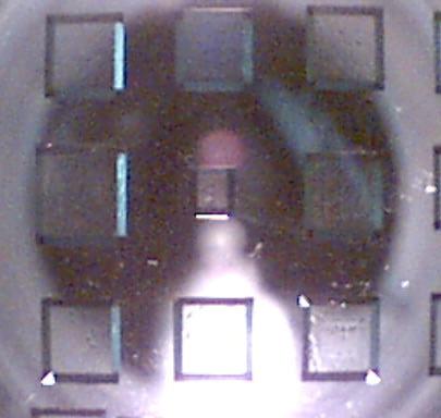
79 PICTURES Page 79


80 PICTURES OF DIAPHRAGM HOLE Page 80

81 PROBE STATION TEST SETUP 5 Volts Vo2=2.5035v R1 R3 R2 R4 Vo1=2.4965v Gnd Apply and release chuck vacuum to observe change in output voltage Page 81
82 Vsupply = 5 Volts PROBE STATION TESTING Turn on Vacuum Chuck (~14.7 psi) R1 R2 Gnd R3 R4 Vo1 Should be volts to ground Vo2 Should be volts to ground Vo1-Vo2 = or 15 mvolts Page 82

83 K&S WAFER SAW Page 83

84 MOUNT CHIP ON TO-8 PACKAGE Fixture to hold TO-8 and TO-39 packages for wire bonding. Page 84

85 WIRE BOND Page 85


86 ATTACH PNEUMATIC FITTING Attach interconnect wires Epoxy to pneumatic fitting Add protective cover Page 86

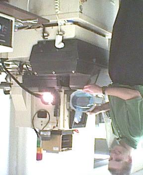
87 PNEUMATIC TEST SET UP Page 87
88 OUTPUT VOLTAGE VERSUS PRESSURE MEMS Pressure Sensor Output Output Voltage (mv) y = x x Pressure (psi) Page 88
89 RESULTS AND CONCLUSION MEMs devices were designed, including Analytical Analysis, Mask Layout Photomasks were made Fabrication process was designed Wafers were processed Completed wafers were tested Chips were packaged Packaged chips were tested Successful Project!!! Page 89
90 ACKNOWLEDGMENTS Page 90
91 REFERENCES 1. Process Development for 3 D Silicon Microstructures, with Application to Mechanical Sensor Devices, Eric Peeters, Katholieke Universiteit Leuven, March 1994.] 2. United States Patent 5,357, S.K. Clark and K.D. Wise, Pressure Sensitivity in Anisotropically Etched Thin-Diaphragm Pressure Sensors, IEEE Transactions on Electron Devices, Vol. ED-26, pp , Page 91
Photoresist Coat, Expose and Develop Laboratory Dr. Lynn Fuller
 ROCHESTER INSTITUTE OF TECHNOLOGY MICROELECTRONIC ENGINEERING Photoresist Coat, Expose and Develop Laboratory Dr. Lynn Fuller Webpage: http://www.rit.edu/lffeee 82 Lomb Memorial Drive Rochester, NY 14623-5604
Bulk MEMS Fabrication Blog 2017 Dr. Lynn Fuller, Casey Gonta, Patsy Cadareanu
 ROCHESTER INSTITUTE OF TECHNOLOGY MICROELECTRONIC ENGINEERING Bulk MEMS Fabrication Blog 2017 Dr. Lynn Fuller, Casey Gonta, Patsy Cadareanu Webpage: http://people.rit.edu/lffeee 82 Lomb Memorial Drive
Microelectromechanical Systems (MEMs) Unit Processes for MEMs Measurement
 Unit Processes for MEMs Measurement") ROCHESTER INSTITUTE OF TEHNOLOGY MICROELECTRONIC ENGINEERING Microelectromechanical Systems (MEMs) Unit Processes for MEMs Measurement Dr. Lynn Fuller Webpage: http://people.rit.edu/lffeee 82 Lomb Memorial
ROCHESTER INSTITUTE OF TEHNOLOGY MICROELECTRONIC ENGINEERING Microelectromechanical Systems (MEMs) Unit Processes for MEMs Measurement Dr. Lynn Fuller Webpage: http://people.rit.edu/lffeee 82 Lomb Memorial
Lab #2 Wafer Cleaning (RCA cleaning)
") Lab #2 Wafer Cleaning (RCA cleaning) RCA Cleaning System Used: Wet Bench 1, Bay1, Nanofabrication Center Chemicals Used: H 2 O : NH 4 OH : H 2 O 2 (5 : 1 : 1) H 2 O : HF (10 : 1) H 2 O : HCl : H 2 O 2
Lab #2 Wafer Cleaning (RCA cleaning) RCA Cleaning System Used: Wet Bench 1, Bay1, Nanofabrication Center Chemicals Used: H 2 O : NH 4 OH : H 2 O 2 (5 : 1 : 1) H 2 O : HF (10 : 1) H 2 O : HCl : H 2 O 2
Chapter 3 Silicon Device Fabrication Technology
 Chapter 3 Silicon Device Fabrication Technology Over 10 15 transistors (or 100,000 for every person in the world) are manufactured every year. VLSI (Very Large Scale Integration) ULSI (Ultra Large Scale
Surface micromachining and Process flow part 1
 Surface micromachining and Process flow part 1 Identify the basic steps of a generic surface micromachining process Identify the critical requirements needed to create a MEMS using surface micromachining
3.155J / 6.152J Micro/Nano Processing Technology TAKE-HOME QUIZ FALL TERM 2005
 3.155J / 6.152J Micro/Nano Processing Technology TAKE-HOME QUIZ FALL TERM 2005 1) This is an open book, take-home quiz. You are not to consult with other class members or anyone else. You may discuss the
Isolation Technology. Dr. Lynn Fuller
 ROCHESTER INSTITUTE OF TECHNOLOGY MICROELECTRONIC ENGINEERING Isolation Technology Dr. Lynn Fuller Motorola Professor 82 Lomb Memorial Drive Rochester, NY 14623-5604 Tel (585) 475-2035 Fax (585) 475-5041
LAM 490 Etch Recipes. Dr. Lynn Fuller
 ROCHESTER INSTITUTE OF TECHNOLOGY MICROELECTRONIC ENGINEERING LAM 490 Etch Recipes Dr. Lynn Fuller Professor, Webpage: http://people.rit.edu/lffeee 82 Lomb Memorial Drive Rochester, NY 14623-5604 Tel (585)
Surface MEMS Fabrication Blog Dr. Lynn Fuller, Adam Wardas Webpage:
 ROCHESTER INSTITUTE OF TECHNOLOGY MICROELECTRONIC ENGINEERING Surface MEMS Fabrication Blog Dr. Lynn Fuller, Adam Wardas Webpage: http://people.rit.edu/lffeee 82 Lomb Memorial Drive Rochester, NY 14623-5604
Photolithography I ( Part 2 )
") 1 Photolithography I ( Part 2 ) Chapter 13 : Semiconductor Manufacturing Technology by M. Quirk & J. Serda Bjørn-Ove Fimland, Department of Electronics and Telecommunication, Norwegian University of Science
1 Photolithography I ( Part 2 ) Chapter 13 : Semiconductor Manufacturing Technology by M. Quirk & J. Serda Bjørn-Ove Fimland, Department of Electronics and Telecommunication, Norwegian University of Science
EECS130 Integrated Circuit Devices
 EECS130 Integrated Circuit Devices Professor Ali Javey 9/13/2007 Fabrication Technology Lecture 1 Silicon Device Fabrication Technology Over 10 15 transistors (or 100,000 for every person in the world)
Lecture 10: MultiUser MEMS Process (MUMPS)
") MEMS: Fabrication Lecture 10: MultiUser MEMS Process (MUMPS) Prasanna S. Gandhi Assistant Professor, Department of Mechanical Engineering, Indian Institute of Technology, Bombay, 1 Recap Various VLSI based
MEMS: Fabrication Lecture 10: MultiUser MEMS Process (MUMPS) Prasanna S. Gandhi Assistant Professor, Department of Mechanical Engineering, Indian Institute of Technology, Bombay, 1 Recap Various VLSI based
Report 1. B. Starting Wafer Specs Number: 10 Total, 6 Device and 4 Test wafers
 Aaron Pederson EE 432 Lab Dr. Meng Lu netid: abp250 Lab instructor: Yunfei Zhao Report 1 A. Overview The goal of this lab is to go through the semiconductor fabrication process from start to finish. This
EE C245 ME C218 Introduction to MEMS Design Fall 2011
 Lecture Outline EE C245 ME C218 Introduction to MEMS Design Fall 2011 Prof. Clark T.-C. Nguyen Dept. of Electrical Engineering & Computer Sciences University of California at Berkeley Berkeley, CA 94720
Microstructures using RF sputtered PSG film as a sacrificial layer in surface micromachining
 Sādhanā Vol. 34, Part 4, August 2009, pp. 557 562. Printed in India Microstructures using RF sputtered PSG film as a sacrificial layer in surface micromachining VIVEKANAND BHATT 1,, SUDHIR CHANDRA 1 and
2015 EE410-LOCOS 0.5µm Poly CMOS Process Run Card Lot ID:
 STEP 0.00 - PHOTOMASK #0- ZERO LEVEL MARKS Starting materials is n-type silicon (5-10 ohm-cm). Add four test wafers labeled T1-T4. T1 and T2 will travel with the device wafers and get all of the processing
EE40 Lec 22. IC Fabrication Technology. Prof. Nathan Cheung 11/19/2009
 Suggested Reading EE40 Lec 22 IC Fabrication Technology Prof. Nathan Cheung 11/19/2009 300mm Fab Tour http://www-03.ibm.com/technology/manufacturing/technology_tour_300mm_foundry.html Overview of IC Technology
Fabrication and Layout
 ECEN454 Digital Integrated Circuit Design Fabrication and Layout ECEN 454 3.1 A Glimpse at MOS Device Polysilicon Aluminum ECEN 475 4.2 1 Material Classification Insulators Glass, diamond, silicon oxide
4/10/2012. Introduction to Microfabrication. Fabrication
 Introduction to Microfabrication Fabrication 1 MEMS Fabrication Flow Basic Process Flow in Micromachining Nadim Maluf, An introduction to Microelectromechanical Systems Engineering 2 Thin Film Deposition
6.777J/2.732J Design and Fabrication of Microelectromechanical Devices Spring Term Solution to Problem Set 2 (16 pts)
") 6.777J/2.732J Design and Fabrication of Microelectromechanical Devices Spring Term 2007 By Brian Taff (Adapted from work by Feras Eid) Solution to Problem Set 2 (16 pts) Issued: Lecture 4 Due: Lecture
6.777J/2.732J Design and Fabrication of Microelectromechanical Devices Spring Term 2007 By Brian Taff (Adapted from work by Feras Eid) Solution to Problem Set 2 (16 pts) Issued: Lecture 4 Due: Lecture
4. Thermal Oxidation. a) Equipment Atmospheric Furnace
 Equipment Atmospheric Furnace") 4. Thermal Oxidation a) Equipment Atmospheric Furnace Oxidation requires precise control of: temperature, T ambient gas, G time spent at any given T & G, t Vito Logiudice 34 4. Thermal Oxidation b) Mechanism
4. Thermal Oxidation a) Equipment Atmospheric Furnace Oxidation requires precise control of: temperature, T ambient gas, G time spent at any given T & G, t Vito Logiudice 34 4. Thermal Oxidation b) Mechanism
Micro-Electro-Mechanical Systems (MEMS) Fabrication. Special Process Modules for MEMS. Principle of Sensing and Actuation
 Fabrication. Special Process Modules for MEMS. Principle of Sensing and Actuation") Micro-Electro-Mechanical Systems (MEMS) Fabrication Fabrication Considerations Stress-Strain, Thin-film Stress, Stiction Special Process Modules for MEMS Bonding, Cavity Sealing, Deep RIE, Spatial forming
Micro-Electro-Mechanical Systems (MEMS) Fabrication Fabrication Considerations Stress-Strain, Thin-film Stress, Stiction Special Process Modules for MEMS Bonding, Cavity Sealing, Deep RIE, Spatial forming
Lecture 5. SOI Micromachining. SOI MUMPs. SOI Micromachining. Silicon-on-Insulator Microstructures. Agenda:
 EEL6935 Advanced MEMS (Spring 2005) Instructor: Dr. Huikai Xie SOI Micromachining Agenda: SOI Micromachining SOI MUMPs Multi-level structures Lecture 5 Silicon-on-Insulator Microstructures Single-crystal
Manufacturing Process
 Digital Integrated Circuits A Design Perspective Jan M. Rabaey Anantha Chandrakasan Borivoje Nikolic Manufacturing Process July 30, 2002 1 CMOS Process 2 A Modern CMOS Process gate-oxide TiSi 2 AlCu Tungsten
Micro-Scale Engineering I Microelectromechanical Systems (MEMS) Y. C. Lee
 Y. C. Lee") Micro-Scale Engineering I Microelectromechanical Systems (MEMS) Y. C. Lee Department of Mechanical Engineering University of Colorado Boulder, CO 80309-0427 leeyc@colorado.edu September 2, 2008 1 Three
Micro-Scale Engineering I Microelectromechanical Systems (MEMS) Y. C. Lee Department of Mechanical Engineering University of Colorado Boulder, CO 80309-0427 leeyc@colorado.edu September 2, 2008 1 Three
Dow Corning WL-5150 Photodefinable Spin-On Silicone
 Dow Corning WL-515 Photodefinable Spin-On Silicone Properties and Processing Procedures Introduction Dow Corning WL-515 is a silicone formulation which can be photopatterned and cured using standard microelectronics
Surface Micromachining
 Surface Micromachining Outline Introduction Material often used in surface micromachining Material selection criteria in surface micromachining Case study: Fabrication of electrostatic motor Major issues
Process Flow in Cross Sections
 Process Flow in Cross Sections Process (simplified) 0. Clean wafer in nasty acids (HF, HNO 3, H 2 SO 4,...) --> wear gloves! 1. Grow 500 nm of SiO 2 (by putting the wafer in a furnace with O 2 2. Coat
Lecture 6. Through-Wafer Interconnect. Agenda: Through-wafer Interconnect Polymer MEMS. Through-Wafer Interconnect -1. Through-Wafer Interconnect -2
 Agenda: EEL6935 Advanced MEMS (Spring 2005) Instructor: Dr. Huikai Xie Lecture 6 Through-wafer Interconnect EEL6935 Advanced MEMS 2005 H. Xie 1/21/2005 1 Motivations: Wafer-level packaging CMOS 3D Integration
Brian Izzio 5th Year Microelectronic Engineering Student. Rochester Institute of Technology
 CAPACITAWZE-VOI~TAGE characterization FOR POLYSILICON GATE MOS CAPACITORS DJTRODUcTION Brian Izzio 5th Year Microelectronic Engineering Student Rochester Institute of Technology ABSTRACT The effects of
Lecture 19 Microfabrication 4/1/03 Prof. Andy Neureuther
 EECS 40 Spring 2003 Lecture 19 Microfabrication 4/1/03 Prof. ndy Neureuther How are Integrated Circuits made? Silicon wafers Oxide formation by growth or deposition Other films Pattern transfer by lithography
How To Write A Flowchart
 1 Learning Objectives To learn how you transfer a device concept into a process flow to fabricate the device in the EKL labs You learn the different components that makes up a flowchart; process blocks,
EE 457 : Multilayer Devices
 March 1, 2010 EE 457 : Multilayer Devices by prepared for: Prof. K. Westra M. Mohammed EE 457: Multilayer Devices Objectives...1 Process Flow...1 1.Cleaning...1 2.Thermal Oxidation...1 3.Aluminum Sputtering...1
Drytech Quad Etch Recipes Dr. Lynn Fuller Mike Aquilino Microelectronic Engineering
 ROCHESTER INSTITUTE OF TECHNOLOGY MICROELECTRONIC ENGINEERING Drytech Quad Etch Recipes Dr. Lynn Fuller Mike Aquilino 82 Lomb Memorial Drive Rochester, NY 14623-5604 Tel (585) 475-2035 Fax (585) 475-5041
Thin. Smooth. Diamond.
 UNCD Wafers Thin. Smooth. Diamond. UNCD Wafers - A Family of Diamond Material UNCD is Advanced Diamond Technologies (ADT) brand name for a family of thin fi lm diamond products. UNCD Aqua The Aqua series
Temperature Scales. Questions. Temperature Conversions 7/21/2010. EE580 Solar Cells Todd J. Kaiser. Thermally Activated Processes
 7/1/010 EE80 Solar Cells Todd J. Kaiser Flow of Wafer in Fabrication Lecture 0 Microfabrication A combination of Applied Chemistry, Physics and ptics Thermal Processes Diffusion & xidation Photolithograpy
CMOS Manufacturing Process
 CMOS Manufacturing Process CMOS Process A Modern CMOS Process gate-oxide TiSi 2 AlCu Tungsten SiO 2 n+ p-well p-epi poly n-well p+ SiO 2 p+ Dual-Well Trench-Isolated CMOS Process Circuit Under Design V
VLSI INTRODUCTION P.VIDYA SAGAR ( ASSOCIATE PROFESSOR) Department of Electronics and Communication Engineering, VBIT
 Department of Electronics and Communication Engineering, VBIT") VLSI INTRODUCTION P.VIDYA SAGAR ( ASSOCIATE PROFESSOR) contents UNIT I INTRODUCTION: Introduction to IC Technology MOS, PMOS, NMOS, CMOS & BiCMOS technologies. BASIC ELECTRICAL PROPERTIES : Basic Electrical
VLSI INTRODUCTION P.VIDYA SAGAR ( ASSOCIATE PROFESSOR) contents UNIT I INTRODUCTION: Introduction to IC Technology MOS, PMOS, NMOS, CMOS & BiCMOS technologies. BASIC ELECTRICAL PROPERTIES : Basic Electrical
LAM4600 Plasma Etch Tool Recipes Dr. Lynn Fuller Webpage:
 ROCHESTER INSTITUTE OF TECHNOLOGY MICROELECTRONIC ENGINEERING LAM4600 Plasma Etch Tool Recipes Webpage: http://people.rit.edu/lffeee 82 Lomb Memorial Drive Rochester, NY 14623-5604 Tel (585) 475-2035 Email:
Figure 2.3 (cont., p. 60) (e) Block diagram of Pentium 4 processor with 42 million transistors (2000). [Courtesy Intel Corporation.
 (e) Block diagram of Pentium 4 processor with 42 million transistors (2000). [Courtesy Intel Corporation.") Figure 2.1 (p. 58) Basic fabrication steps in the silicon planar process: (a) oxide formation, (b) selective oxide removal, (c) deposition of dopant atoms on wafer, (d) diffusion of dopant atoms into exposed
Figure 2.1 (p. 58) Basic fabrication steps in the silicon planar process: (a) oxide formation, (b) selective oxide removal, (c) deposition of dopant atoms on wafer, (d) diffusion of dopant atoms into exposed
Semiconductor Manufacturing Technology. IC Fabrication Process Overview
 Semiconductor Manufacturing Technology Michael Quirk & Julian Serda October 00 by Prentice Hall Chapter 9 IC Fabrication Process Overview /4 Objectives After studying the material in this chapter, you
Applications of High-Performance MEMS Pressure Sensors Based on Dissolved Wafer Process
 Applications of High-Performance MEMS Pressure Sensors Based on Dissolved Wafer Process Srinivas Tadigadapa and Sonbol Massoud-Ansari Integrated Sensing Systems (ISSYS) Inc., 387 Airport Industrial Drive,
CMOS Manufacturing process. Circuit designer. Design rule set. Process engineer. Set of optical masks. Fabrication process.
 CMOS Manufacturing process Circuit design Set of optical masks Fabrication process Circuit designer Design rule set Process engineer All material: Chap. 2 of J. Rabaey, A. Chandrakasan, B. Nikolic, Digital
DuPont MX5000 Series
 DuPont MX5000 Series DATA SHEET & PROCESSING INFORMATION High Performance Multi-Purpose Polymer Film for MEMS Applications PRODUCT FEATURES/ APPLICATIONS Negative working, aqueous processable dry film
Regents of the University of California
 Surface-Micromachining Process Flow Photoresist Sacrificial Oxide Structural Polysilcon Deposit sacrificial PSG: Target = 2 m 1 hr. 40 min. LPCVD @450 o C Densify the PSG Anneal @950 o C for 30 min. Lithography
Colorado School of Mines PHGN/CHGN 435. Modules 1 and 2. Authors: Garrick Johnson Trevor Haak Carl DuBois Ethan Palay
 Colorado School of Mines PHGN/CHGN 435 Modules 1 and 2 Authors: Garrick Johnson Trevor Haak Carl DuBois Ethan Palay February 10, 2015 1 Introduction and Background Integrated circuits are an integral part
Intel Pentium Processor W/MMX
 Construction Analysis Intel Pentium Processor W/MMX Report Number: SCA 9706-540 Global Semiconductor Industry the Serving Since 1964 15022 N. 75th Street Scottsdale, AZ 85260-2476 Phone: 602-998-9780 Fax:
There are basically two approaches for bulk micromachining of. silicon, wet and dry. Wet bulk micromachining is usually carried out
 57 Chapter 3 Fabrication of Accelerometer 3.1 Introduction There are basically two approaches for bulk micromachining of silicon, wet and dry. Wet bulk micromachining is usually carried out using anisotropic
UV5 POSITIVE DUV PHOTORESIST For Microlithography Applications
 UV5 POSITIVE DUV PHOTORESIST For Microlithography Applications DESCRIPTION UV5 positive DUV photoresist has been optimized to provide vertical profile imaging of isolated and semidense features for device
Semiconductor Technology
 Semiconductor Technology from A to Z Oxidation www.halbleiter.org Contents Contents List of Figures List of Tables II III 1 Oxidation 1 1.1 Overview..................................... 1 1.1.1 Application...............................
Via Fill in Small Trenches using Hot Aluminum Process. By Alice Wong
 Via Fill in Small Trenches using Hot Aluminum Process By Alice Wong Goals for Project Good Via Fill in Small contact holes using hot aluminum process Be able to get good images of the contact holes using
MEMS LAB MANUAL. Matthew Leone Todd Kaiser Montana State University. Special Thanks to: Andy Lingley Brad Pierson Phil Himmer
 MEMS LAB MANUAL 2007 A complete description of the fabrication sequence for piezoresistive MEMS sensors. This manual was designed for use with the Montana Microfabrication Facility at MSU. Special Thanks
SURFACE MICROMACHINING
 SURFACE MICROMACHINING Features are built up, layer by layer on the surface of a substrate. Surface micromachined devices are much smaller than bulk micromachined components. Nature of deposition process
HOMEWORK 4 and 5. March 15, Homework is due on Monday March 30, 2009 in Class. Answer the following questions from the Course Textbook:
 HOMEWORK 4 and 5 March 15, 2009 Homework is due on Monday March 30, 2009 in Class. Chapter 7 Answer the following questions from the Course Textbook: 7.2, 7.3, 7.4, 7.5, 7.6*, 7.7, 7.9*, 7.10*, 7.16, 7.17*,
5.8 Diaphragm Uniaxial Optical Accelerometer
 5.8 Diaphragm Uniaxial Optical Accelerometer Optical accelerometers are based on the BESOI (Bond and Etch back Silicon On Insulator) wafers, supplied by Shin-Etsu with (100) orientation, 4 diameter and
Fabrication Technology
 Fabrication Technology By B.G.Balagangadhar Department of Electronics and Communication Ghousia College of Engineering, Ramanagaram 1 OUTLINE Introduction Why Silicon The purity of Silicon Czochralski
UV5 POSITIVE DUV PHOTORESIST For DUV Applications
 UV5 POSITIVE DUV PHOTORESIST For DUV Applications DESCRIPTION UV5 positive DUV photo resist has been optimized to provide vertical profile imaging of isolated and semidense features for device production
Silicon Wafer Processing PAKAGING AND TEST
 Silicon Wafer Processing PAKAGING AND TEST Parametrical test using test structures regularly distributed in the wafer Wafer die test marking defective dies dies separation die fixing (not marked as defective)
SU-8 Overhanging Structures Using a Photoresist Sacrificial Layer and Embedded Aluminum Mask
 SU-8 Overhanging Structures Using a Photoresist Sacrificial Layer and Embedded Aluminum Mask By: See-Ho Tsang, Dan Sameoto, Sae-Won Lee A MAJOR PROJECT REPORT SUBMITTED IN PARTIAL FULLFILLMENT FOR ENGINEERING
Low-temperature, Simple and Fast Integration Technique of Microfluidic Chips by using a UV-curable Adhesive
 Low-temperature, Simple and Fast Integration Technique of Microfluidic Chips by using a UV-curable Adhesive Supplementary Information Channel fabrication Glass microchannels. A borosilicate glass wafer
INTERVIA BPP-10 Photoresist
 Technical Data Sheet INTERVIA BPP-10 Photoresist For Advanced Packaging Applications Description Regional Product Availability Advantages INTERVIA BPP-10 Photoresist is a general-purpose, multi-wavelength
Uncrosslinked SU-8 as a sacrificial material
 INSTITUTE OFPHYSICS PUBLISHING JOURNAL OF MICROMECHANICS AND MICROENGINEERING J. Micromech. Microeng. 15 (2005) N1 N5 doi:10.1088/0960-1317/15/1/n01 TECHNICAL NOTE Uncrosslinked as a sacrificial material
Lecture 22: Integrated circuit fabrication
 Lecture 22: Integrated circuit fabrication Contents 1 Introduction 1 2 Layering 4 3 Patterning 7 4 Doping 8 4.1 Thermal diffusion......................... 10 4.2 Ion implantation.........................
Plasma-Enhanced Chemical Vapor Deposition
 Plasma-Enhanced Chemical Vapor Deposition Steven Glenn July 8, 2009 Thin Films Lab 4 ABSTRACT The objective of this lab was to explore lab and the Applied Materials P5000 from a different point of view.
CMOS FABRICATION. n WELL PROCESS
 CMOS FABRICATION n WELL PROCESS Step 1: Si Substrate Start with p- type substrate p substrate Step 2: Oxidation Exposing to high-purity oxygen and hydrogen at approx. 1000 o C in oxidation furnace SiO
Semiconductor Device Fabrication Study
 Proceedings of The National Conference on Undergraduate Research (NCUR) 2003 University of Utah, Salt Lake City, Utah March 13-15, 2003 Semiconductor Device Fabrication Study Tsung-Ta Ho and Michael R.
Reclaimed Silicon Solar Cells
 61 Reclaimed Silicon Solar Cells Victor Prajapati. Department ofmicroelectronic Engineering, 82 Lomb Memorial Dr., Rochester, NY 14623. Email: Victor.Prajapati@gmail.com Abstract Fully processed CMOS Si
R&D ACTIVITIES AT ASSCP-BHEL,GURGAON IN SOLAR PV. DST-EPSRC Workshop on Solar Energy Research
 R&D ACTIVITIES AT -BHEL,GURGAON IN SOLAR PV at the DST-EPSRC Workshop on Solar Energy Research (22 nd 23 rd April, 2009) by Dr.R.K. Bhogra, Addl. General Manager & Head Email: cpdrkb@bhel.co.in Dr.A.K.
CMOS LAB MANUAL CMOS LAB MANUAL
 CMOS LAB MANUAL 2011 CMOS LAB MANUAL This manual was designed for use with the Montana Microfabrication Facility at MSU. The intention of the manual is to provide lab users and MSU students with a complete
Piezoresistance in Silicon. Dr. Lynn Fuller Webpage:
 ROCHESTER INSTITUTE OF TECHNOLOGY MICROELECTRONIC ENGINEERING Piezoresistance in Silicon Webpage: http://people.rit.edu/lffeee 82 Lomb Memorial Drive Rochester, NY 14623-5604 Tel (585) 475-2035 Email:
AZ BARLi II Solvent Compatible Bottom Antireflective Coating for i-line Process Data Package
 AZ BARLi II Solvent Compatible Bottom Antireflective Coating for i-line Process Data Package The information contained herein is, as far as we are aware, true and accurate. However, no representations
KGC SCIENTIFIC Making of a Chip
 KGC SCIENTIFIC www.kgcscientific.com Making of a Chip FROM THE SAND TO THE PACKAGE, A DIAGRAM TO UNDERSTAND HOW CPU IS MADE? Sand CPU CHAIN ANALYSIS OF SEMICONDUCTOR Material for manufacturing process
FABRICATION of MOSFETs
 FABRICATION of MOSFETs CMOS fabrication sequence -p-type silicon substrate wafer -creation of n-well regions for pmos transistors, -impurity implantation into the substrate. -thick oxide is grown in the
Etching Etching Definitions Isotropic Etching: same in all direction Anisotropic Etching: direction sensitive Selectivity: etch rate difference
 Etching Etching Definitions Isotropic Etching: same in all direction Anisotropic Etching: direction sensitive Selectivity: etch rate difference between 2 materials Need strong selectivity from masking
Overview of CMP for TSV Applications. Robert L. Rhoades, Ph.D. Presentation for AVS Joint Meeting June 2013 San Jose, CA
 Overview of CMP for TSV Applications Robert L. Rhoades, Ph.D. Presentation for AVS Joint Meeting June 2013 San Jose, CA Outline TSV s and the Role of CMP TSV Pattern and Fill TSV Reveal (non-selective)
EE 330 Lecture 9. IC Fabrication Technology Part II. -Oxidation -Epitaxy -Polysilicon -Planarization -Resistance and Capacitance in Interconnects
 EE 330 Lecture 9 IC Fabrication Technology Part II -Oxidation -Epitaxy -Polysilicon -Planarization -Resistance and Capacitance in Interconnects Review from Last Time Etching Dry etch (anisotropic) SiO
Lecture 7 CMOS MEMS. CMOS MEMS Processes. CMOS MEMS Processes. Why CMOS-MEMS? Agenda: CMOS MEMS: Fabrication. MEMS structures can be made
 EEL6935 Advanced MEMS (Spring 2005) Instructor: Dr. Huikai Xie CMOS MEMS Agenda: Lecture 7 CMOS MEMS: Fabrication Pre-CMOS Intra-CMOS Post-CMOS Deposition Etching Why CMOS-MEMS? Smart on-chip CMOS circuitry
Investigation of ProTEX PSB Thin Film as Photosensitive Layer for MEMS capacitive pressure sensor diaphragm based Si/SiC Wafer
 Investigation of ProTEX PSB Thin Film as Photosensitive Layer for MEMS capacitive pressure sensor diaphragm based Si/SiC Wafer Author Marsi, Noraini, Majlis, Burhanuddin Yeop, Hamzah, Azrul Azlan, Mohd-Yasin,
Plasma Etching Rates & Gases Gas ratios affects etch rate & etch ratios to resist/substrate
 Plasma Etching Rates & Gases Gas ratios affects etch rate & etch ratios to resist/substrate Development of Sidewalls Passivating Films Sidewalls get inert species deposited on them with plasma etch Creates
Rapid Thermal Processing (RTP) Dr. Lynn Fuller
 Dr. Lynn Fuller") ROCHESTER INSTITUTE OF TECHNOLOGY MICROELECTRONIC ENGINEERING Rapid Thermal Processing (RTP) Dr. Lynn Fuller Webpage: http://people.rit.edu/lffeee 82 Lomb Memorial Drive Rochester, NY 14623-5604 Tel (585)
ROCHESTER INSTITUTE OF TECHNOLOGY MICROELECTRONIC ENGINEERING Rapid Thermal Processing (RTP) Dr. Lynn Fuller Webpage: http://people.rit.edu/lffeee 82 Lomb Memorial Drive Rochester, NY 14623-5604 Tel (585)
SU Permanent Epoxy Negative Photoresist PROCESSING GUIDELINES FOR:
 SU-8 2000 Permanent Epoxy Negative Photoresist PROCESSING GUIDELINES FOR: SU-8 2100 and SU-8 2150 www.microchem.com SU-8 2000 is a high contrast, epoxy based photoresist designed for micromachining and
Ion Implantation Most modern devices doped using ion implanters Ionize gas sources (single +, 2+ or 3+ ionization) Accelerate dopant ions to very
 Accelerate dopant ions to very") Ion Implantation Most modern devices doped using ion implanters Ionize gas sources (single +, 2+ or 3+ ionization) Accelerate dopant ions to very high voltages (10-600 KeV) Use analyzer to selection charge/mass
Ion Implantation Most modern devices doped using ion implanters Ionize gas sources (single +, 2+ or 3+ ionization) Accelerate dopant ions to very high voltages (10-600 KeV) Use analyzer to selection charge/mass
Microfabrication of Heterogeneous, Optimized Compliant Mechanisms SUNFEST 2001 Luo Chen Advisor: Professor G.K. Ananthasuresh
 Microfabrication of Heterogeneous, Optimized Compliant Mechanisms SUNFEST 2001 Luo Chen Advisor: Professor G.K. Ananthasuresh Fig. 1. Single-material Heatuator with selective doping on one arm (G.K. Ananthasuresh)
Advanced CMOS Process Technology Part 3 Dr. Lynn Fuller
 MICROELECTRONIC ENGINEERING ROCHESTER INSTITUTE OF TECHNOLOGY Part 3 Dr. Lynn Fuller Webpage: http://people.rit.edu/lffeee Electrical and Microelectronic Engineering Rochester Institute of Technology 82
MCC. PMGI Resists NANO PMGI RESISTS OFFER RANGE OF PRODUCTS
 MCC PMGI RESISTS OFFER Sub.25µm lift-off processing Film thicknesses from 5µm Choice of resin blends for optimal undercut control High thermal stability Superior adhesion to Si, NiFe, GaAs, InP
125nXT Series. EMD PeRFoRmaNce MaTeRIaLs. technical datasheet. Photopolymer Negative Tone Photoresists APPLICATION TYPICAL PROCESS THICKNESS GRADES
 EMD PeRFoRmaNce MaTeRIaLs technical datasheet AZ 125nXT Series Photopolymer Negative Tone Photoresists APPLICATION Thick photopolymer photoresists featuring aspect ratios and photospeed not possible with
PROCESSING OF INTEGRATED CIRCUITS
 PROCESSING OF INTEGRATED CIRCUITS Overview of IC Processing (Part I) Silicon Processing Lithography Layer Processes Use in IC Fabrication (Part II) Integrating the Fabrication Steps IC Packaging (Part
9-11 April 2008 Micro-electroforming Metallic Bipolar Electrodes for Mini-DMFC Stacks
 9-11 April 8 Micro-electroforming Metallic Bipolar Electrodes for Mini-DMFC Stacks R. F. Shyu 1, H. Yang, J.-H. Lee 1 Department of Mechanical Manufacturing Engineering, National Formosa University, Yunlin,
Ajay Kumar Gautam [VLSI TECHNOLOGY] VLSI Technology for 3RD Year ECE/EEE Uttarakhand Technical University
![Ajay Kumar Gautam [VLSI TECHNOLOGY] VLSI Technology for 3RD Year ECE/EEE Uttarakhand Technical University](/thumbs/75/72824557.jpg "Ajay Kumar Gautam [VLSI TECHNOLOGY] VLSI Technology for 3RD Year ECE/EEE Uttarakhand Technical University") 2014 Ajay Kumar Gautam [VLSI TECHNOLOGY] VLSI Technology for 3RD Year ECE/EEE Uttarakhand Technical University Page1 Syllabus UNIT 1 Introduction to VLSI Technology: Classification of ICs, Scale of integration,
2014 Ajay Kumar Gautam [VLSI TECHNOLOGY] VLSI Technology for 3RD Year ECE/EEE Uttarakhand Technical University Page1 Syllabus UNIT 1 Introduction to VLSI Technology: Classification of ICs, Scale of integration,
Thermal Evaporation. Theory
 Thermal Evaporation Theory 1. Introduction Procedures for depositing films are a very important set of processes since all of the layers above the surface of the wafer must be deposited. We can classify
micro resist technology
 Characteristics Processing guidelines Negative Tone Photoresist Series ma-n 1400 ma-n 1400 is a negative tone photoresist series designed for the use in microelectronics and microsystems. The resists are
Processing Procedures for CYCLOTENE 3000 Series Dry Etch Resins
 Revised: April 2008 Processing Procedures for CYCLOTENE 3000 Series Dry Etch Resins 1. INTRODUCTION The CYCLOTENE 3000 series Advanced Electronic Resins derived from B-staged bisbenzocyclobutene (BCB)
Cost of Integrated Circuits
 Cost of IC Design 1 Cost of Integrated Circuits NRE (Non-Recurrent Engineering) costs fixed design time and effort, mask generation independent of sales volume / number of products one-time cost factor
UV6 POSITIVE DUV PHOTORESIST For DUV Applications
 UV6 POSITIVE DUV PHOTORESIST For DUV Applications DESCRIPTION UV6 Positive DUV Photoresist has been optimized to provide vertical profile imaging of dense and semi-isolated features for device production
National Semiconductor LM2672 Simple Switcher Voltage Regulator
 Construction Analysis National Semiconductor LM2672 Simple Switcher Voltage Regulator Report Number: SCA 9712-570 Global Semiconductor Industry the Serving Since 1964 17350 N. Hartford Drive Scottsdale,
OPTICAL, ELECTRICAL AND STRUCTURAL PROPERTIES OF PECVD QUASI EPITAXIAL PHOSPHOROUS DOPED SILICON FILMS ON CRYSTALLINE SILICON SUBSTRATE
 OPTICAL, ELECTRICAL AN STRUCTURAL PROPERTIES OF PECV QUASI EPITAXIAL PHOSPHOROUS OPE SILICON FILMS ON CRYSTALLINE SILICON SUBSTRATE Mahdi Farrokh-Baroughi, Hassan El-Gohary, and Siva Sivoththaman epartment
FABRICATION ENGINEERING MICRO- NANOSCALE ATTHE AND. Fourth Edition STEPHEN A. CAMPBELL. of Minnesota. University OXFORD UNIVERSITY PRESS
 AND FABRICATION ENGINEERING ATTHE MICRO- NANOSCALE Fourth Edition STEPHEN A. CAMPBELL University of Minnesota New York Oxford OXFORD UNIVERSITY PRESS CONTENTS Preface xiii prrt i OVERVIEW AND MATERIALS
Avatrel Stress Buffer Coatings: Low Stress Passivation and Redistribution Applications
 Avatrel Stress Buffer Coatings: Low Stress Passivation and Redistribution Applications Ed Elce, Chris Apanius, Jeff Krotine, Jim Sperk, Andrew Bell, Rob Shick* Sue Bidstrup-Allen, Paul Kohl Takashi Hirano,
Dallas Semicoductor DS80C320 Microcontroller
 Construction Analysis Dallas Semicoductor DS80C320 Microcontroller Report Number: SCA 9702-525 Global Semiconductor Industry the Serving Since 1964 15022 N. 75th Street Scottsdale, AZ 85260-2476 Phone: