Flash Memory with Nanoparticle Floating Gates
|
|
|
- Julius Singleton
- 6 years ago
- Views:
Transcription
1 Flash Memory with Nanoparticle Floating Gates Sanjay Banerjee Director, Microelectronics Research Center Cockrell Chair Professor of Electrical & Computer Engineering University of Texas at Austin Why Nanoparticles in Flash Memory Self-assembly schemes Device Performance Acknowledgements: DARPA MARCO, NSF NIRT, Micron


 Dust mite 200")


 0.")


2 The Scale of Things Nanometers and More Things Natural 10-2 m 1 cm 10 mm Things Manmade Head of a pin 1-2 mm The Challenge Ant ~ 5 mm 10-3 m 1,000,000 nanometers = 1 millimeter (mm) Dust mite 200 μm Human hair ~ μm wide Red blood cells with white cell ~ 2-5 μm ~10 nm diameter Fly ash ~ μm ATP synthase Nanoworld Microworld 10-4 m 10-5 m 10-6 m 10-7 m 10-8 m Ultraviolet Visible Infrared Microwave 0.1 mm 100 μm 0.01 mm 10 μm 1,000 nanometers = 1 micrometer (μm) 0.1 μm 100 nm Smaller is different 0.01 μm 10 nm Pollen grain Red blood cells Zone plate x-ray lens Outer ring spacing ~35 nm Self-assembled, Nature-inspired structure Many 10s of nm MicroElectroMechanical (MEMS) devices μm wide Nanotube electrode O O S O O O O O O O O O O O S O S O S O S P O O Fabricate and combine nanoscale building blocks to make useful devices, e.g., a photosynthetic reaction center with integral semiconductor storage. O O S O O S O S DNA ~2-1/2 nm diameter Atoms of silicon spacing ~tenths of nm 10-9 m m Soft x-ray 1 nanometer (nm) More is different 0.1 nm Quantum corral of 48 iron atoms on copper surface positioned one at a time with an STM tip Corral diameter 14 nm Carbon buckyball ~1 nm diameter Carbon nanotube ~1.3 nm diameter Office of Basic Energy Sciences Office of Science, U.S. DOE Version , pmd

3 Moore s Law No exponential is forever! But can we delay forever? source drain


4 Flash memory applications Markets Consumer Electronics Networking Wireless Industrial Control Automotive Floating gate Control Gate Tunnel dielectric
5 NAND Flash Market Segmentation Digital Settop Box 0% Others 5% *Others include GPS, games, emerging applications, etc MP3 players (Flash based) 22% $468 M 2005 NAND Demand TAM Percentage isupply: Q $2124 M USB Flash Drive 17% $1667 M $5230 M Removable Solid State Flash Cards 53% $244 M $70 M Mobile Handset (Embedded) 2% Digital Still Camera (Embedded) 1% NOR Flash had TAM of 7B$, mostly in wireless cell phones. Very high growth rates!!!


 High")
6 Flash Technology Scaling History 1986 / 1.5μm 1988 / 1.0μm 1991 / 0.8μm 1993 / 0.6μm 1996 / 0.4μm 1/~ / 0.25μm 2000 / 0.18μm 2002 / 0.13μm 2004 / 90nm 2006 / 65nm 10X 10X 10X Volume Production Year / Technology Generation Source: Intel Flash Invented in mid 1980 s NOR flash evolved from EPROM NAND started as poly-poly erase cell later evolving to present structure ~20 years & 10 Generations of ETOX (Intel NOR) High Volume Production 8+ years & 5 Generations of MLC: 2bit / cell

7 NVM- Long Term Requirements (ITRS 2006)

8 Nanoparticle Gate Flash Memory Gate Gate Source Drain Source Drain Conventional Flash Memory A defect totally discharges the floating gate Nano-floating Gate Memory A defect discharges only one dot Thick tunnel oxide High voltage/ power Low reliability/ speed High-k tunnel oxide Speed/ power/ density better Reliability improved New phenomena- self-assembly, Coulomb blockade, multi-level cells
 showing SiGe dots")


9 SiGe Nanocrystals on High-K Dielectrics HfO 2 SiO 2 AFM scans (1 micron x 1micron) showing SiGe dots grown at ~ 500ºC for 90 s with 0.75 gas ratio of GeH 4 to Si 2 H 6. Kim., Banerjee, Growth of germanium quantum dots on different dielectric substrates by chemical-vapor deposition, J VAC SCI TECHNOL B 19 (4): 2001
10 Band diagram of HfO 2 and SiO 2 dielectric at low program voltage Nanocrystal Dots Si E c Channel SiGe E c Channel Dot gate Dot Interface oxide gate Tunneling oxide (HfO 2 ) (HfO 2 ) SiO 2 F-N tunneling (due to small φ b ) Tunneling oxide (SiO 2 ) (SiO 2 ) J g [A/cm 2 ] HfO 2 E.O.T 4nm Direct tunneling Direct tunneling V G [V]
11 Program & Erase Transient Characteristics Threshold Voltage shift (V) HfO 2 tunneling oixde =4.8nm SiO 2 tunneling oxide = 3.6nm Erase Program HfO 2 2.5V SiO 2 4V SiO 2 4V HfO 2 2.5V ΔV th (V) HfO 2 tunneling oxide SiO 2 tunneling oxide Without dots With SiGe dots Without dots Program/Erase Time (s) V CG (V) Kim DW, Kim T, Banerjee SK, ELECTRON DEV 50 (9): SEP 2003


12 The Bio-nanometer Perspective Atom Water DNA Virus Protein Bacterium Cells Hair Fish egg Human eye nm μm Nanomaterials: Nanotubes Dendrimers Nanopores Quantum dots Nanoshells Nanoparticles mm Gate/ Transistor Interconnect Integrated circuit Microprocessor dielectrics/substrate Slide by C. Li

")

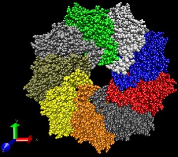
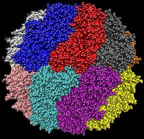
13 Yamashita, IEDM 2006, p. 447 (Ferritin) Ishii, Nature Vol. 423, 2003 (Chaperonin)
 and Semiconductor")
 NCs Schematic structure of")
14 Protein assembly of Metal (Co, Au,..) and Semiconductor (PbSe, CdSe, Ge..) NCs Schematic structure of Chaperonin 60 (GroEL)


15 STEM images of PbSe nanocrystals on SiO 2 50 nm 50 nm Without chaperonin template With chaperonin template Various semiconductor and metal nanocrystals self-assembled, including Co Density~ cm -2
 B C D ΔV FB (V) 0.8 Program/Erase time=1s 0.6 0.4 0.2 0.")
16 ΔV FB comparison of protein-mediated PbSe NC MOS capacitor and control samples TaN Gate Control Oxide Tunnel Oxide Si Substrate NCs SiO 2 10 nm PbSe NCs TaN Si A PbSe NCs Protein Template (Annealed) B C D ΔV FB (V) 0.8 Program/Erase time=1s A B C,D Program Voltage (V)
17 Endurance and Retention Characteristics V FB (V) PbSe -10V 200ms Co -8V 200ms PbSe 10V 200ms Co 8V 200ms Number of Cycles V FB (V) PbSe -10V 200ms Co -8V 200ms PbSe 10V 200ms Co 8V 200ms Retention Time (s) Devices survived 10 5 cycles of program/erase operation; no sign of window closure Devices have good retention.


18 Heat Shock Proteins (Trent, NASA)
 1.")

19 Coulomb Blockade in SiGe dot on SiO 2 and HfO 2 2.0x10⁻⁵ SiGe on SiO 520 ºC Drain Current (A) 1.5x x x10-6 n=0 n=1 0.0 SiO 2 tunneling oxide = 3.6nm Gate Voltage (V)
 Device mesa n + Source/Drain Schematic side view Scanning Electron")
20 Vertical Flash Memory Sidewall channels Nanocrystal floating gate Gate Source Drain contact Gate poly Source contact (outside view) Device mesa n + Source/Drain Schematic side view Scanning Electron Micrograph

21 Vertical Flash Retention at 300K ± 9 V, 100 ms tunneling P/E 10 nm E1237 PCL_ _VFR5W4_04_3DFlash_Nanocrystals.dm3 MAG: 295kX
22 Nanoparticle Self-Assembly Using PS-b-PMMA PMMA Copolymer Process Flow Employing a sandwich of organic/ inorganic/ organic layers (Polyimide/ SiO 2 / PS-b-PMMA) to engineer the aspect ratio of the patterns Material Characterization (a) (b) 100 nm 100 nm (c) (d) glue 6 Normalized Count 100 nm 10nm Si Substrate Nickel Nanocrystals SEM micrographs of (a) Copolymer template, (b) transferred polymer patterns into the underlying SiO2 layer, (c) ultimate array of Ni nanoparticles. (d) Cross-sectional image of the embedded nanoparticles within SiO 2. Histogram of the copolymer pore size distribution shown in Fig. (a)
23 Characteristics of MOSCAP Memory Devices ±10V, 100 msec ±8V, 100 msec Control Sample - w/ o Ni dots 10V 8V 6V Gate Voltage (V) ΔV FB (V) Write/ Erase time (s) High frequency C-V 1MHz Memory window for different program voltages Transient characteristics of the memory device

24 Molecular Memories, Misra, IEDM p ; IEDM p Variability, DOS? SONOS trap densities ~10 19 cm -3 ev -1 For ~3 nm layer, ~3X10 12 cm -2 traps spatially and energetically distributed


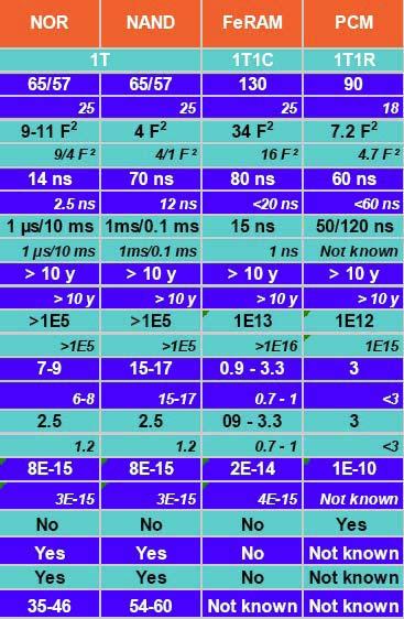
25 Non-MOS Memory Contenders (adapted from Fazio, Intel) MRAM FeRAM Phase Change Cell Size λ 2 Large ~40 20 Large ~25 Small ~6.5 CMOS <200C Post Magnetic Fe reduces in hydrogen Compatible with backend Integration Tight MJT control Etching difficult for Fe CMOS metal processing Read Write Cycling Endurance Scalability Application Color Code Poor OK Good Non-Destructive, Fast, Low Power Power constrained, Scales poorly; half select issue Theoretically Infinite Write current increases with scaling, materials engineering required at each scaling node; superparamagnetic limit? Embedded Working Memory Low Density Destructive: Endurance limited read Low power capacitive Theoretically good speed 1e-8 1e12; claims made, but limited data 3D cell required sub 90nm. Material engineering required at each scaling node Embedded Low Power Low Density Non-Destructive, Moderate speed, Scales poorly Power constrained, large drivers, Improves with scaling ~1e12; claims made, but limited data; Erratic failures No material changes, No physical limits known down to ~5nm Stand Alone or Embedded High Density Low Cost Data Storage Region Chalcogenide Phase Change Material Amorphous Poly Crystalline Heater Resistive Electrode
26 1R
27 Nanocrystal Dots Channel Dot gate Tunneling oxide End-of-roadmap (2020, L=6 nm) NAND F= 14 nm, Tox= 6 nm, Cell area ~ 1000 nm 2; (3X for NOR) NC spacing ~ tunnel oxide thickness ~ 4 nm Spacing & NC size/dos affects charge capture crosssection & Read Optimal spacing depends on dielectric & NC band diagram, retention (10 8 s), Erase/Write times (10-6 s) E barr = 1eV For NC densities of ~ cm -2, room for ~10 NC Variability is a challenge for NC & trap-based cells Self-assembly and non-planar structures?
28 There is plenty of room at the bottom! Feynman Will these devices make it? The answer is a very definite.. Maybe!!
Nanotechnology for Molecular and Cellular Manipulation
 Nanotechnology for Molecular and Cellular Manipulation Logan Liu Micro and Nano Technology Lab Department of Electrical & Computer Engineering University of Illinois Physical Systems Nano vs. Bio Micro
1 Thin-film applications to microelectronic technology
 1 Thin-film applications to microelectronic technology 1.1 Introduction Layered thin-film structures are used in microelectronic, opto-electronic, flat panel display, and electronic packaging technologies.
Annual Meeting. North Carolina State University Dr. Veena Misra. January 17 19, 2017 December
 Annual Meeting North Carolina State University Dr. Veena Misra January 17 19, 2017 December 8 2015 1 Misra Group at NCSU Over 9 years experience in wide band gap research on SiC, GaN and Ga2O3. World leaders
From microelectronics down to nanotechnology.
 From microelectronics down to nanotechnology sami.franssila@tkk.fi Contents Lithography: scaling x- and y-dimensions MOS transistor physics Scaling oxide thickness (z-dimension) CNT transistors Conducting
Vertical Group IV Nanowires: Potential Enablers for 3D Integration and BioFET Sensor Arrays
 Vertical Group IV Nanowires: Potential Enablers for 3D Integration and BioFET Sensor Arrays Paul C. McIntyre Department of Materials Science & Engineering Geballe Laboratory for Advanced Materials Stanford
ENS 06 Paris, France, December 2006
 CARBON NANOTUBE ARRAY VIAS FOR INTERCONNECT APPLICATIONS Jyh-Hua ng 1, Ching-Chieh Chiu 2, Fuang-Yuan Huang 2 1 National Nano Device Laboratories, No.26, Prosperity Road I, Science-Based Industrial Park,
Vertically aligned Ni magnetic nanowires fabricated by diblock-copolymer-directed Al thin film anodization
 Vertically aligned Ni magnetic nanowires fabricated by diblock-copolymer-directed Al thin film anodization Researcher: Kunbae (Kevin) Noh, Graduate Student, MAE Dept. and CMRR Collaborators: Leon Chen,
Nanosilicon single-electron transistors and memory
 Nanosilicon single-electron transistors and memory Z. A. K. Durrani (1, 2) and H. Ahmed (3) (1) Electronic Devices and Materials Group, Engineering Department, University of Cambridge, Trumpington Street,
VLSI INTRODUCTION P.VIDYA SAGAR ( ASSOCIATE PROFESSOR) Department of Electronics and Communication Engineering, VBIT
 Department of Electronics and Communication Engineering, VBIT") VLSI INTRODUCTION P.VIDYA SAGAR ( ASSOCIATE PROFESSOR) contents UNIT I INTRODUCTION: Introduction to IC Technology MOS, PMOS, NMOS, CMOS & BiCMOS technologies. BASIC ELECTRICAL PROPERTIES : Basic Electrical
VLSI INTRODUCTION P.VIDYA SAGAR ( ASSOCIATE PROFESSOR) contents UNIT I INTRODUCTION: Introduction to IC Technology MOS, PMOS, NMOS, CMOS & BiCMOS technologies. BASIC ELECTRICAL PROPERTIES : Basic Electrical
Advanced Gate Stack, Source/Drain, and Channel Engineering for Si-Based CMOS 6: New Materials, Processes, and Equipment
 Advanced Gate Stack, Source/Drain, and Channel Engineering for Si-Based CMOS 6: New Materials, Processes, and Equipment Editors: E. P. Gusev Qualcomm MEMS Technologies San Jose, California, USA D-L. Kwong
Lecture 19 Microfabrication 4/1/03 Prof. Andy Neureuther
 EECS 40 Spring 2003 Lecture 19 Microfabrication 4/1/03 Prof. ndy Neureuther How are Integrated Circuits made? Silicon wafers Oxide formation by growth or deposition Other films Pattern transfer by lithography
Nagatsuta, Midori-ku, Yokohama , Japan. Technology, 4259-S2-20 Nagatsuta, Midori-ku, Yokohama , Japan
 Improvement of Interface Properties of W/La O 3 /Si MOS Structure Using Al Capping Layer K. Tachi a, K. Kakushima b, P. Ahmet a, K. Tsutsui b, N. Sugii b, T. Hattori a, and H. Iwai a a Frontier Collaborative
MOS Gate Dielectrics. Outline
 MOS Gate Dielectrics Outline Scaling issues Technology Reliability of SiO 2 Nitrided SiO 2 High k dielectrics 42 Incorporation of N or F at the Si/SiO 2 Interface Incorporating nitrogen or fluorine instead
High-Resolution, Electrohydrodynamic Inkjet Printing of Stretchable, Metal Oxide Semiconductor Transistors with High Performances
 Electronic Supplementary Material (ESI) for Nanoscale. This journal is The Royal Society of Chemistry 2016 ` Electronic Supplementary Information High-Resolution, Electrohydrodynamic Inkjet Printing of
EE40 Lec 22. IC Fabrication Technology. Prof. Nathan Cheung 11/19/2009
 Suggested Reading EE40 Lec 22 IC Fabrication Technology Prof. Nathan Cheung 11/19/2009 300mm Fab Tour http://www-03.ibm.com/technology/manufacturing/technology_tour_300mm_foundry.html Overview of IC Technology
Lecture 4. Oxidation (applies to Si and SiC only) Reading: Chapter 4
 Reading: Chapter 4") Lecture 4 Oxidation (applies to Si and SiC only) Reading: Chapter 4 Introduction discussion: Oxidation: Si (and SiC) Only The ability to grow a high quality thermal oxide has propelled Si into the forefront
Lecture 4 Oxidation (applies to Si and SiC only) Reading: Chapter 4 Introduction discussion: Oxidation: Si (and SiC) Only The ability to grow a high quality thermal oxide has propelled Si into the forefront
National Semiconductor LM2672 Simple Switcher Voltage Regulator
 Construction Analysis National Semiconductor LM2672 Simple Switcher Voltage Regulator Report Number: SCA 9712-570 Global Semiconductor Industry the Serving Since 1964 17350 N. Hartford Drive Scottsdale,
Visit
 Practical Applications for Nano- Electronics by Vimal Gopee E-mail: Vimal.gopee@npl.co.uk 10/10/12 Your Delegate Webinar Control Panel Open and close your panel Full screen view Raise hand for Q&A at the
MARORA A Plasma Selective-oxidation Apparatus for Metal-gate Devices
 Hitachi Review Vol. 57 (2008), No. 3 127 MARORA A Plasma Selective-oxidation Apparatus for Metal-gate Devices Tadashi Terasaki Masayuki Tomita Katsuhiko Yamamoto Unryu Ogawa, Dr. Eng. Yoshiki Yonamoto,
Project III. 4: THIN FILM DEVICES FOR LARGE AREA ELECTRONICS
 Project III. 4: THIN FILM DEVICES FOR LARGE AREA ELECTRONICS Project leader: Dr D.N. Kouvatsos Collaborating researchers from other projects: Dr D. Davazoglou Ph.D. candidates: M. Exarchos, L. Michalas
CMOS FABRICATION. n WELL PROCESS
 CMOS FABRICATION n WELL PROCESS Step 1: Si Substrate Start with p- type substrate p substrate Step 2: Oxidation Exposing to high-purity oxygen and hydrogen at approx. 1000 o C in oxidation furnace SiO
Intel Pentium Processor W/MMX
 Construction Analysis Intel Pentium Processor W/MMX Report Number: SCA 9706-540 Global Semiconductor Industry the Serving Since 1964 15022 N. 75th Street Scottsdale, AZ 85260-2476 Phone: 602-998-9780 Fax:
Nanofabrication Prof. Stephen Y. Chou NanoStructure Laboratory
 Nanofabrication Prof. Stephen Y. Chou Department of Electrical Engineering Princeton University 1 Acknowledgment Dr. Paul Fischer Dr. Yun Wang Dr. Jay Guo Dr. Peter Klauss Dr. Jim Wang Dr. Longtin He Dr.
Nano Computers through Nanotechnology
 International Journal of Education and Science Research Review E-ISSN 2348-6457 Volume-2, Issue-1 February- 2015 P-ISSN 2348-1817 Nano Computers through Nanotechnology Laith R.Fleih, Taghreed M. Younis
2006 UPDATE METROLOGY
 INTERNATIONAL TECHNOLOGY ROADMAP FOR SEMICONDUCTORS METROLOGY THE ITRS DEVED AND INTENDED FOR TECHNOLOGY ASSESSMENT ONLY AND WITHOUT REGARD TO ANY COMMERCIAL CONSIDERATIONS PERTAINING TO INDIVIDUAL PRODUCTS
Workshop on Nanoscience and Catalysts March 2008, QAU, Islamabad Nanocomposites for Thermal management Applications
 Fazal Ahmad Khalid Pro-Rector GIK Institute of Engineering Sciences and Technology Topi, NWFP, Pakistan (Khalid@giki.edu.pk) Workshop on Nanoscience and Catalysts 24-25 March 2008, QAU, Islamabad Nanocomposites
Memory Devices. Ki-Nam Kim, President, Institut of Technology Samsung Electronics, 2010 IEDM, San Francisco.
 Memory Devices In Korea now, Samsung : 2010, 30nm 2Gb DDRS DRAM/DDR3 SRAM 2011, Invest US $12 bil. for 20nm & SysLSI. Hynix : 2010, 26nm MLC- NAND Flash 2011, 30nm 4Gb DRAM At 2020, the demands of computing
Fabrication and Layout
 ECEN454 Digital Integrated Circuit Design Fabrication and Layout ECEN 454 3.1 A Glimpse at MOS Device Polysilicon Aluminum ECEN 475 4.2 1 Material Classification Insulators Glass, diamond, silicon oxide
VLSI Systems and Computer Architecture Lab
 ΚΥΚΛΩΜΑΤΑ VLSI Πανεπιστήμιο Ιωαννίνων CMOS Technology Τμήμα Μηχανικών Η/Υ και Πληροφορικής 1 From the book: An Introduction ti to VLSI Process By: W. Maly ΚΥΚΛΩΜΑΤΑ VLSI Διάρθρωση 1. N well CMOS 2. Active
Semiconductor Manufacturing Technology. IC Fabrication Process Overview
 Semiconductor Manufacturing Technology Michael Quirk & Julian Serda October 00 by Prentice Hall Chapter 9 IC Fabrication Process Overview /4 Objectives After studying the material in this chapter, you
Figure 2.3 (cont., p. 60) (e) Block diagram of Pentium 4 processor with 42 million transistors (2000). [Courtesy Intel Corporation.
 (e) Block diagram of Pentium 4 processor with 42 million transistors (2000). [Courtesy Intel Corporation.") Figure 2.1 (p. 58) Basic fabrication steps in the silicon planar process: (a) oxide formation, (b) selective oxide removal, (c) deposition of dopant atoms on wafer, (d) diffusion of dopant atoms into exposed
Figure 2.1 (p. 58) Basic fabrication steps in the silicon planar process: (a) oxide formation, (b) selective oxide removal, (c) deposition of dopant atoms on wafer, (d) diffusion of dopant atoms into exposed
Motorola PC603R Microprocessor
 Construction Analysis Motorola PC603R Microprocessor Report Number: SCA 9709-551 Global Semiconductor Industry the Serving Since 1964 17350 N. Hartford Drive Scottsdale, AZ 85255 Phone: 602-515-9780 Fax:
FABRICATION ENGINEERING MICRO- NANOSCALE ATTHE AND. Fourth Edition STEPHEN A. CAMPBELL. of Minnesota. University OXFORD UNIVERSITY PRESS
 AND FABRICATION ENGINEERING ATTHE MICRO- NANOSCALE Fourth Edition STEPHEN A. CAMPBELL University of Minnesota New York Oxford OXFORD UNIVERSITY PRESS CONTENTS Preface xiii prrt i OVERVIEW AND MATERIALS
EE 434 Lecture 9. IC Fabrication Technology
 EE 434 Lecture 9 IC Fabrication Technology Quiz 7 The layout of a film resistor with electrodes A and B is shown. If the sheet resistance of the film is 40 /, determine the resistance between nodes A and
EE 560 FABRICATION OF MOS CIRCUITS. Kenneth R. Laker, University of Pennsylvania
 1 EE 560 FABRICATION OF MOS CIRCUITS 2 CMOS CHIP MANUFACTRING STEPS Substrate Wafer Wafer Fabrication (diffusion, oxidation, photomasking, ion implantation, thin film deposition, etc.) Finished Wafer Wafer
Hitachi A 64Mbit (8Mb x 8) Dynamic RAM
 Dynamic RAM") Construction Analysis Hitachi 5165805A 64Mbit (8Mb x 8) Dynamic RAM Report Number: SCA 9712-565 Global Semiconductor Industry the Serving Since 1964 17350 N. Hartford Drive Scottsdale, AZ 85255 Phone:
Construction Analysis Hitachi 5165805A 64Mbit (8Mb x 8) Dynamic RAM Report Number: SCA 9712-565 Global Semiconductor Industry the Serving Since 1964 17350 N. Hartford Drive Scottsdale, AZ 85255 Phone:
Lecture 030 Integrated Circuit Technology - I (5/8/03) Page 030-1
 Page 030-1") Lecture 030 Integrated Circuit Technology - I (5/8/03) Page 030-1 LECTURE 030 INTEGRATED CIRCUIT TECHNOLOGY - I (References [7,8]) Objective The objective of this presentation is: 1.) Illustrate integrated
Lecture 030 Integrated Circuit Technology - I (5/8/03) Page 030-1 LECTURE 030 INTEGRATED CIRCUIT TECHNOLOGY - I (References [7,8]) Objective The objective of this presentation is: 1.) Illustrate integrated
Non-charge Storage Resistive Memory: How it works
 Accelerating the next technology revolution Non-charge Storage Resistive Memory: How it works Gennadi Bersuker Copyright 2009 SEMATECH, Inc. SEMATECH, and the SEMATECH logo are registered servicemarks
Nanosensors. Rachel Heil 12/7/07 Wentworth Institute of Technology Department of Electronics and Mechanical Professor Khabari Ph.D.
 Nanosensors Rachel Heil 12/7/07 Wentworth Institute of Technology Department of Electronics and Mechanical Professor Khabari Ph.D. There are many advances in nanotechnology that if perfected could help
Electrical Characteristics of Rare Earth (La, Ce, Pr and Tm) Oxides/Silicates Gate Dielectric
 Oxides/Silicates Gate Dielectric") Electrical Characteristics of Rare Earth (La, Ce, Pr and Tm) Oxides/Silicates Gate Dielectric K. Matano 1, K. Funamizu 1, M. Kouda 1, K. Kakushima 2, P. Ahmet 1, K. Tsutsui 2, A. Nishiyama 2, N. Sugii
Electrical Characteristics of Rare Earth (La, Ce, Pr and Tm) Oxides/Silicates Gate Dielectric K. Matano 1, K. Funamizu 1, M. Kouda 1, K. Kakushima 2, P. Ahmet 1, K. Tsutsui 2, A. Nishiyama 2, N. Sugii
SGS-Thomson M17C1001 1Mb UVEPROM
 Construction Analysis SGS-Thomson M17C1001 1Mb UVEPROM Report Number: SCA 9612-518 Global Semiconductor Industry the Serving Since 1964 15022 N. 75th Street Scottsdale, AZ 85260-2476 Phone: 602-998-9780
FOR SEMICONDUCTORS 2009 EDITION
 INTERNATIONAL TECHNOLOGY ROADMAP FOR SEMICONDUCTORS 2009 EDITION FRONT END PROCESSES THE ITRS IS DEVISED AND INTENDED FOR TECHNOLOGY ASSESSMENT ONLY AND IS WITHOUT REGARD TO ANY COMMERCIAL CONSIDERATIONS
Yung-Hui Yeh, and Bo-Cheng Kung Display Technology Center (DTC), Industrial Technology Research Institute, Hsinchu 310, Taiwan
, Industrial Technology Research Institute, Hsinchu 310, Taiwan") Amorphous In 2 O 3 -Ga 2 O 3 -ZnO Thin Film Transistors and Integrated Circuits on Flexible and Colorless Polyimide Substrates Hsing-Hung Hsieh, and Chung-Chih Wu* Graduate Institute of Electronics Engineering,
Amorphous In 2 O 3 -Ga 2 O 3 -ZnO Thin Film Transistors and Integrated Circuits on Flexible and Colorless Polyimide Substrates Hsing-Hung Hsieh, and Chung-Chih Wu* Graduate Institute of Electronics Engineering,
Growth and Doping of SiC-Thin Films on Low-Stress, Amorphous Si 3 N 4 /Si Substrates for Robust Microelectromechanical Systems Applications
 Journal of ELECTRONIC MATERIALS, Vol. 31, No. 5, 2002 Special Issue Paper Growth and Doping of SiC-Thin Films on Low-Stress, Amorphous Si 3 N 4 /Si Substrates for Robust Microelectromechanical Systems
VLSI Technology. By: Ajay Kumar Gautam
 By: Ajay Kumar Gautam Introduction to VLSI Technology, Crystal Growth, Oxidation, Epitaxial Process, Diffusion Process, Ion Implantation, Lithography, Etching, Metallization, VLSI Process Integration,
Isolation Technology. Dr. Lynn Fuller
 ROCHESTER INSTITUTE OF TECHNOLOGY MICROELECTRONIC ENGINEERING Isolation Technology Dr. Lynn Fuller Motorola Professor 82 Lomb Memorial Drive Rochester, NY 14623-5604 Tel (585) 475-2035 Fax (585) 475-5041
Silicon Wafer Processing PAKAGING AND TEST
 Silicon Wafer Processing PAKAGING AND TEST Parametrical test using test structures regularly distributed in the wafer Wafer die test marking defective dies dies separation die fixing (not marked as defective)
Supplementary Figure S1 Crystal structure of the conducting filaments in sputtered SiO 2
 Supplementary Figure S1 Crystal structure of the conducting filaments in sputtered SiO 2 based devices. (a) TEM image of the conducting filament in a SiO 2 based memory device used for SAED analysis. (b)
EEC 118 Lecture #5: MOS Fabrication. Rajeevan Amirtharajah University of California, Davis Jeff Parkhurst Intel Corporation
 EEC 118 Lecture #5: MOS Fabrication Rajeevan Amirtharajah University of California, Davis Jeff Parkhurst Intel Corporation Announcements Lab 3 this week, report due next week HW 3 due this Friday at 4
Roll-to-roll Vacuum Processing of Organic Thin Film Transistors
 Roll-to-roll Vacuum Processing of Organic Thin Film Transistors Hazel Assender Department of Materials University of Oxford DALMATIAN TECHNOLOGY 1 Aim of the Research To demonstrate the ability to fabricate
Portland Technology Development, * CR, # QRE, % PTM Intel Corporation
 A 45nm Logic Technology with High-k + Metal Gate Transistors, Strained Silicon, 9 Cu Interconnect Layers, 193nm Dry Patterning, and 100% Pb-free Packaging K. Mistry, C. Allen, C. Auth, B. Beattie, D. Bergstrom,
VLSI Technology Dr. Nandita Dasgupta Department of Electrical Engineering Indian Institute of Technology, Madras
 VLSI Technology Dr. Nandita Dasgupta Department of Electrical Engineering Indian Institute of Technology, Madras Lecture - 33 Problems in LOCOS + Trench Isolation and Selective Epitaxy So, we are discussing
Interface Structure and Charge Trapping in HfO 2 -based MOSFETS
 Interface Structure and Charge Trapping in HfO 2 -based MOSFETS MURI - ANNUAL REVIEW, 13 and 14 th May 2008 S.K. Dixit 1, 2, T. Feng 6 X.J. Zhou 3, R.D. Schrimpf 3, D.M. Fleetwood 3,4, S.T. Pantelides
Amorphous Oxide Transistor Electrokinetic Reflective Display on Flexible Glass
 Amorphous Oxide Transistor Electrokinetic Reflective Display on Flexible Glass Devin A. Mourey, Randy L. Hoffman, Sean M. Garner *, Arliena Holm, Brad Benson, Gregg Combs, James E. Abbott, Xinghua Li*,
CMOS Manufacturing process. Circuit designer. Design rule set. Process engineer. Set of optical masks. Fabrication process.
 CMOS Manufacturing process Circuit design Set of optical masks Fabrication process Circuit designer Design rule set Process engineer All material: Chap. 2 of J. Rabaey, A. Chandrakasan, B. Nikolic, Digital
Dallas Semicoductor DS80C320 Microcontroller
 Construction Analysis Dallas Semicoductor DS80C320 Microcontroller Report Number: SCA 9702-525 Global Semiconductor Industry the Serving Since 1964 15022 N. 75th Street Scottsdale, AZ 85260-2476 Phone:
CMOS Manufacturing Process
 CMOS Manufacturing Process CMOS Process A Modern CMOS Process gate-oxide TiSi 2 AlCu Tungsten SiO 2 n+ p-well p-epi poly n-well p+ SiO 2 p+ Dual-Well Trench-Isolated CMOS Process Circuit Under Design V
FORMING-FREE NITROGEN-DOPED ALUMINUM OXIDE RESISTIVE RANDOM ACCESS MEMORY GROWN BY ATOMIC LAYER DEPOSITION TECHNIQUE A DISSERTATION
 FORMING-FREE NITROGEN-DOPED ALUMINUM OXIDE RESISTIVE RANDOM ACCESS MEMORY GROWN BY ATOMIC LAYER DEPOSITION TECHNIQUE A DISSERTATION SUBMITTED TO THE DEPARTMENT OF ELECTRICAL ENGINEERING AND THE COMMITTEE
Atomic Layer Deposition of Novel High Dielectric Constant Materials
 Atomic Layer Deposition of Novel High Dielectric Constant Materials Adam Kueltzo # & Julie Lam * Thornton Fractional North High School # and Maine East High School * August 2, 2007 University of Illinois
During solution evaporation, there are two major competing evaporation-driven effects, coffee ring effect and Marangoni flow.
 Abstract Evaporation driven particle packing has been investigated to reveal interesting patterns at micrometer to millimeter scale. While the microscopic structures of these patterns are well characterized,
Lecture 22: Integrated circuit fabrication
 Lecture 22: Integrated circuit fabrication Contents 1 Introduction 1 2 Layering 4 3 Patterning 7 4 Doping 8 4.1 Thermal diffusion......................... 10 4.2 Ion implantation.........................
Rockwell R RF to IF Down Converter
 Construction Analysis Rockwell R6732-13 RF to IF Down Converter Report Number: SCA 9709-552 Global Semiconductor Industry the Serving Since 1964 17350 N. Hartford Drive Scottsdale, AZ 85255 Phone: 602-515-9780
Process steps for Field Emitter devices built on Silicon wafers And 3D Photovoltaics on Silicon wafers
 Process steps for Field Emitter devices built on Silicon wafers And 3D Photovoltaics on Silicon wafers David W. Stollberg, Ph.D., P.E. Research Engineer and Adjunct Faculty GTRI_B-1 Field Emitters GTRI_B-2
Impact of Filament Evolution on Reliability Issues of Oxide Electrolyte Based Conductive Bridge Random Access Memory
 Impact of Filament Evolution on Reliability Issues of Oxide Electrolyte Based Conductive Bridge Random Access Memory Hangbing Lv, Xiaoxin Xu, Hongtao Liu, Qing Luo, Qi Liu, Shibing Long, Ming Liu* Institute
Poly-SiGe MEMS actuators for adaptive optics
 Poly-SiGe MEMS actuators for adaptive optics Blake C.-Y. Lin a,b, Tsu-Jae King a, and Richard S. Muller a,b a Department of Electrical Engineering and Computer Sciences, b Berkeley Sensor and Actuator
Lattice isplsi1032e CPLD
 Construction Analysis Lattice isplsi1032e CPLD Report Number: SCA 9612-522 Global Semiconductor Industry the Serving Since 1964 15022 N. 75th Street Scottsdale, AZ 85260-2476 Phone: 602-998-9780 Fax: 602-948-1925
Silver Diffusion Bonding and Layer Transfer of Lithium Niobate to Silicon
 Chapter 5 Silver Diffusion Bonding and Layer Transfer of Lithium Niobate to Silicon 5.1 Introduction In this chapter, we discuss a method of metallic bonding between two deposited silver layers. A diffusion
March 10th. Frog, Water Strider, Gecko. Elephant vs. Ant Design & Manufacturing II. Ask Dave and Pat. Spring Quiz 1 on March 17 th MEMS I
 P O O O O O O O O O O O O O O O O O O O O O O O S S S S S S S S Office of Basic Energy Sciences Office of Science, U.S. DOE Version 03-05-02 2.008 Design & Manufacturing II Spring 2004 MEMS I March 10th
Hei Wong.
 Defects and Disorders in Hafnium Oxide and at Hafnium Oxide/Silicon Interface Hei Wong City University of Hong Kong Email: heiwong@ieee.org Tokyo MQ2012 1 Outline 1. Introduction, disorders and defects
Fabrication of Ru/Bi 4-x La x Ti 3 O 12 /Ru Ferroelectric Capacitor Structure Using a Ru Film Deposited by Metalorganic Chemical Vapor Deposition
 Mat. Res. Soc. Symp. Proc. Vol. 784 2004 Materials Research Society C7.7.1 Fabrication of Ru/Bi 4-x La x Ti 3 O 12 /Ru Ferroelectric Capacitor Structure Using a Ru Film Deposited by Metalorganic Chemical
Ajay Kumar Gautam [VLSI TECHNOLOGY] VLSI Technology for 3RD Year ECE/EEE Uttarakhand Technical University
![Ajay Kumar Gautam [VLSI TECHNOLOGY] VLSI Technology for 3RD Year ECE/EEE Uttarakhand Technical University](/thumbs/75/72824557.jpg "Ajay Kumar Gautam [VLSI TECHNOLOGY] VLSI Technology for 3RD Year ECE/EEE Uttarakhand Technical University") 2014 Ajay Kumar Gautam [VLSI TECHNOLOGY] VLSI Technology for 3RD Year ECE/EEE Uttarakhand Technical University Page1 Syllabus UNIT 1 Introduction to VLSI Technology: Classification of ICs, Scale of integration,
2014 Ajay Kumar Gautam [VLSI TECHNOLOGY] VLSI Technology for 3RD Year ECE/EEE Uttarakhand Technical University Page1 Syllabus UNIT 1 Introduction to VLSI Technology: Classification of ICs, Scale of integration,
Interconnects. Outline. Interconnect scaling issues Aluminum technology Copper technology. Properties of Interconnect Materials
 Interconnects Outline Interconnect scaling issues Aluminum technology Copper technology 1 Properties of Interconnect Materials Metals Silicides Barriers Material Thin film Melting resistivity point ( C)
Aligned Carbon Nanofibre-Polymer Composite Membranes. CNT Growth and Manipulation. Eleanor Campbell Dept. of Physics, Göteborg University
 Aligned Carbon Nanofibre-Polymer Composite Membranes CNT Growth and Manipulation Eleanor Campbell Dept. of Physics, Göteborg University Plasma CVD Growth Polymer/Nanofibre Composite Low ambient temperature
Thin Films: Sputtering Systems (Jaeger Ch 6 & Ruska Ch 7,) Can deposit any material on any substrate (in principal) Start with pumping down to high
 Can deposit any material on any substrate (in principal) Start with pumping down to high") Thin Films: Sputtering Systems (Jaeger Ch 6 & Ruska Ch 7,) Can deposit any material on any substrate (in principal) Start with pumping down to high vacuum ~10-7 torr Removes residual gases eg oxygen from
Thin Films: Sputtering Systems (Jaeger Ch 6 & Ruska Ch 7,) Can deposit any material on any substrate (in principal) Start with pumping down to high vacuum ~10-7 torr Removes residual gases eg oxygen from
nanosilicon Nanophotonics
 nanosilicon Nanophotonics Lorenzo Pavesi Universita di Trento Italy Outline Silicon Photonics NanoSilicon photonics Silicon Nanophotonics NanoSilicon Nanophotonics Conclusion Outline Silicon Photonics
Al 2 O 3 SiO 2 stack with enhanced reliability
 Al 2 O 3 SiO 2 stack with enhanced reliability M. Lisiansky, a A. Fenigstein, A. Heiman, Y. Raskin, and Y. Roizin Tower Semiconductor Ltd., P.O. Box 619, Migdal HaEmek 23105, Israel L. Bartholomew and
Schottky Tunnel Contacts for Efficient Coupling of Photovoltaics and Catalysts
 Schottky Tunnel Contacts for Efficient Coupling of Photovoltaics and Catalysts Christopher E. D. Chidsey Department of Chemistry Stanford University Collaborators: Paul C. McIntyre, Y.W. Chen, J.D. Prange,
EE-612: Lecture 28: Overview of SOI Technology
 EE-612: Lecture 28: Overview of SOI Technology Mark Lundstrom Electrical and Computer Engineering Purdue University West Lafayette, IN USA Fall 2006 NCN www.nanohub.org Lundstrom EE-612 F06 1 outline 1)
Cathodoluminescence measurements of suboxide band-tail and Si dangling bond states at ultrathin Si SiO 2 interfaces
 Cathodoluminescence measurements of suboxide band-tail and Si dangling bond states at ultrathin Si SiO 2 interfaces A. P. Young a) Department of Electrical Engineering, The Ohio State University, Columbus,
HOMEWORK 4 and 5. March 15, Homework is due on Monday March 30, 2009 in Class. Answer the following questions from the Course Textbook:
 HOMEWORK 4 and 5 March 15, 2009 Homework is due on Monday March 30, 2009 in Class. Chapter 7 Answer the following questions from the Course Textbook: 7.2, 7.3, 7.4, 7.5, 7.6*, 7.7, 7.9*, 7.10*, 7.16, 7.17*,
Metallization deposition and etching. Material mainly taken from Campbell, UCCS
 Metallization deposition and etching Material mainly taken from Campbell, UCCS Application Metallization is back-end processing Metals used are aluminum and copper Mainly involves deposition and etching,
Manufacturing Process
 Digital Integrated Circuits A Design Perspective Jan M. Rabaey Anantha Chandrakasan Borivoje Nikolic Manufacturing Process July 30, 2002 1 CMOS Process 2 A Modern CMOS Process gate-oxide TiSi 2 AlCu Tungsten
3D Vertical RRAM. Henry (Hong-Yu) Chen, H.-S. Philip Wong Stanford University, CA, USA Collaborator: Peking University, China
 Chen, H.-S. Philip Wong Stanford University, CA, USA Collaborator: Peking University, China") 3D Vertical RRAM Henry (Hong-Yu) Chen, H.-S. Philip Wong hongyuc@stanford.edu Stanford University, CA, USA Collaborator: Peking University, China Santa Clara, CA 1 What is RRAM? 0 : High Resistance State
3D Vertical RRAM Henry (Hong-Yu) Chen, H.-S. Philip Wong hongyuc@stanford.edu Stanford University, CA, USA Collaborator: Peking University, China Santa Clara, CA 1 What is RRAM? 0 : High Resistance State
Oxide Growth. 1. Introduction
 Oxide Growth 1. Introduction Development of high-quality silicon dioxide (SiO2) has helped to establish the dominance of silicon in the production of commercial integrated circuits. Among all the various
Design, Fabrication, and Characterization of Nano-scale Cross-Point Hafnium Oxide-Based Resistive Random Access Memory
 Design, Fabrication, and Characterization of Nano-scale Cross-Point Hafnium Oxide-Based Resistive Random Access Memory A Thesis Presented to The Academic Faculty By Noah Ellis In Partial Fulfillment Of
Manufacturer Part Number. Module 2: CMOS FEOL Analysis
 Manufacturer Part Number description Module 2: CMOS FEOL Analysis Manufacturer Device # 2 Some of the information is this report may be covered by patents, mask and/or copyright protection. This report
CHAPTER 1 HOW SEMICONDUCTOR CHIPS ARE MADE
 CHAPTER 1 HOW SEMICONDUCTOR CHIPS ARE MADE Hwaiyu Geng Hewlett-Packard Company Palo Alto, California Lin Zhou Intel Corporation Hillsboro, Oregon 1.1 INTRODUCTION Over the past decades, an information
Metallization. Typical current density ~10 5 A/cm 2 Wires introduce parasitic resistance and capacitance
 Metallization Interconnects Typical current density ~10 5 A/cm 2 Wires introduce parasitic resistance and capacitance RC time delay Inter-Metal Dielectric -Prefer low dielectric constant to reduce capacitance
Visualization and Control of Particulate Contamination Phenomena in a Plasma Enhanced CVD Reactor
 Visualization and Control of Particulate Contamination Phenomena in a Plasma Enhanced CVD Reactor Manabu Shimada, 1 Kikuo Okuyama, 1 Yutaka Hayashi, 1 Heru Setyawan, 2 and Nobuki Kashihara 2 1 Department
Thin Films: Sputtering Systems (Jaeger Ch 6 & Ruska Ch 7,) Sputtering: gas plasma transfers atoms from target to substrate Can deposit any material
 Sputtering: gas plasma transfers atoms from target to substrate Can deposit any material") Thin Films: Sputtering Systems (Jaeger Ch 6 & Ruska Ch 7,) Sputtering: gas plasma transfers atoms from target to substrate Can deposit any material on any substrate (in principal) Start with pumping down
Thin Films: Sputtering Systems (Jaeger Ch 6 & Ruska Ch 7,) Sputtering: gas plasma transfers atoms from target to substrate Can deposit any material on any substrate (in principal) Start with pumping down
Metallization. Typical current density ~105 A/cm2 Wires introduce parasitic resistance and capacitance
 Metallization Interconnects Typical current density ~105 A/cm2 Wires introduce parasitic resistance and capacitance RC time delay Inter-Metal Dielectric -Prefer low dielectric constant to reduce capacitance
Hydrothermal Synthesis of Nano-sized PbTiO3 Powder and Epitaxial Film for Memory Capacitor Application
 American Journal of Materials Science and Technology (2012) 1: 22-27 doi:10.7726/ajmst.2012.1004 Research Article Hydrothermal Synthesis of Nano-sized PbTiO3 Powder and Epitaxial Film for Memory Capacitor
Nanotechnology and Nanosensors. Project Title: Electronic skin. Student: Catherine Katsikalaki. Prof: Hossam Haick
 Nanotechnology and Nanosensors Project Title: Electronic skin Student: Catherine Katsikalaki Prof: Hossam Haick 1 Table of Contents Cover page 1 Table of contents 2 Abstract 3 Introduction 4 Literature
Morphology of Thin Aluminum Film Grown by DC Magnetron Sputtering onto SiO 2 on Si(100) Substrate
 Substrate") Morphology of Thin Aluminum Film Grown by DC Magnetron Sputtering onto SiO 2 on Si(1) Substrate Fan Wu Microelectronics Center, Medtronic Inc., Tempe, AZ 85261 James E. Morris Department of Electrical
Morphology of Thin Aluminum Film Grown by DC Magnetron Sputtering onto SiO 2 on Si(1) Substrate Fan Wu Microelectronics Center, Medtronic Inc., Tempe, AZ 85261 James E. Morris Department of Electrical
Technology. Semiconductor Manufacturing. Hong Xiao INTRODUCTION TO SECOND EDITION SPIE PRESS
 INTRODUCTION TO Semiconductor Manufacturing Technology SECOND EDITION Hong Xiao TECHNISCHE INFORMATIONSBiBUOTHEK UNIVERSITATSBIBLIOTHEK HANNOVER SPIE PRESS Bellingham,Washington USA Contents Preface to
Making III-V contact with silicon substrates
 106Technology focus: III-Vs on silicon Making III-V contact with silicon substrates High-speed logic, high-frequency/high-power transistors and photonics systems could benefit from marrying with silicon
200mm Next Generation MEMS Technology update. Florent Ducrot
 200mm Next Generation MEMS Technology update Florent Ducrot The Most Exciting Industries on Earth Semiconductor Display Solar 20,000,000x reduction in COST PER TRANSISTOR in 30 years 1 20x reduction in
State of the art quality of a GeOx interfacial passivation layer formed on Ge(001)
") APPLICATION NOTE State of the art quality of a Ox interfacial passivation layer formed on (001) Summary A number of research efforts have been made to realize Metal-Oxide-Semiconductor Field Effect Transistors
APPLICATION NOTE State of the art quality of a Ox interfacial passivation layer formed on (001) Summary A number of research efforts have been made to realize Metal-Oxide-Semiconductor Field Effect Transistors
Plasma Etching Rates & Gases Gas ratios affects etch rate & etch ratios to resist/substrate
 Plasma Etching Rates & Gases Gas ratios affects etch rate & etch ratios to resist/substrate Development of Sidewalls Passivating Films Sidewalls get inert species deposited on them with plasma etch Creates