Study of transport properties and defect density profile in nanocrystalline silicon germanium devices
|
|
|
- Beverly Singleton
- 6 years ago
- Views:
Transcription

1 Graduate Theses and Dissertations Graduate College 2015 Study of transport properties and defect density profile in nanocrystalline silicon germanium devices Siva Konduri Iowa State University Follow this and additional works at: Part of the Electrical and Electronics Commons Recommended Citation Konduri, Siva, "Study of transport properties and defect density profile in nanocrystalline silicon germanium devices" (2015). Graduate Theses and Dissertations This Dissertation is brought to you for free and open access by the Graduate College at Iowa State University Digital Repository. It has been accepted for inclusion in Graduate Theses and Dissertations by an authorized administrator of Iowa State University Digital Repository. For more information, please contact
2 Study of transport properties and defect density profile in nanocrystalline silicon germanium devices by Siva Konduri A thesis submitted to the graduate faculty in partial fulfillment of the requirements for the degree of DOCTOR OF PHILOSOPHY Major: Electrical Engineering Program of Study Committee: Vikram Dalal, Major Professor Rana Biswas Sumit Chaudhary Joseph Shinar Mani Mina Iowa State University Ames, Iowa 2015 Copyright Siva Konduri, All rights reserved.
3 ii TABLE OF CONTENTS LIST OF FIGURES LIST OF TABLES ACKNOWLEDGEMENTS ABSTRACT iv viii ix x Chapter 1. INTRODUCTION Solar Energy Thin Film Technologies Amorphous Silicon Alloys Nanocrystalline Silicon Alloys Emerging Technologies Structure of the Thesis 7 Chapter 2. LITERATURE SURVEY Nanocrystalline Silicon Growth Mechanism Material Properties Defects in nc-si:h Nanocrystalline Silicon Germanium Material Growth Device Performance Motivation 30 Chapter 3. GROWTH AND CHARACTERIZATION Fabrication Process Plasma Enhanced Chemical Vapor Deposition (PECVD) Sample Preparation Sputtering Measurement Techniques Optical Spectroscopy Raman Spectroscopy X-ray Diffraction (XRD) Energy Dispersive X-ray Spectroscopy (EDS) Space Charge Limited Current (SCLC) Current-Voltage (IV) Characteristics Quantum Efficiency (QE) Measurements Capacitance-Voltage (CV) Measurement Capacitance Frequency (CF) Measurement Capacitance-Frequency vs. Temperature (CFT) Measurements 53 Chapter 4. RESULTS Film Properties Grain Growth Mobility Measurements 60
4 iii Control of Crystallinity Elemental Analysis Absorption Spectra Device Structure and Characterization Hydrogen Profile Power Grading Device Performance Defects in Solar Cells Validation using a-si:h Solar Cells Defect Density Profile of nc-si:h Solar Cells Defect Density Profile of nc-sige:h Solar Cells 82 Chapter 5. CONCLUSION Summary Future Work 90 BIBLIOGRAPHY 91 APPENDIX A 105 Grain Growth and Mobility in Nanocrystalline Ge Films 105 Influence of Oxygen Contamination on Minority Carrier Lifetime and Defect Density in Nanocrystalline Si 112 Defects and Doping in Nanocrystalline Silicon-Germanium Devices 115 APPENDIX B 123 Defect Density Profile of Perovskite Solar Cells 123
5 iv LIST OF FIGURES Figure 1.1 Solar photovoltaic global capacity in the last decade [1]... 2 Figure 1.2 Schematic illustration of different forms of Silicon [3]... 3 Figure 1.3 Absorption spectra for various thin-film materials used in solar cells [10]... 5 Figure 1.4 TEM image of growth of nc-si:h showing conical growth [13]... 6 Figure 1.5 Investment risk vs. maturity for different solar cell technologies [35]... 7 Figure 2.1 The microstructure of nc-si:h at different crystalline volume fractions [13]... 9 Figure 2.2 Schematic concept for the dissociation processes of SiH4 and H2 molecules in the plasma [49] Figure 2.3 Surface diffusion model for the growth of ncsi:h material [54] Figure 2.4 Etching model for the growth of ncsi:h material [54] Figure 2.5 Chemical anneal model for the growth of ncsi:h material [54] Figure 2.6 Schematic diagram of ncsi:h material with density of states [58] Figure 2.7 (a) Material phase diagram [13] and (b) Depth profile with crystallinity in nc-si:h films [60] Figure 2.8 (a) Crystallinity with thickness of the film, (b) Enhancement in the device performance of cell with power grading technique [61] Figure 2.9 Schematic diagram of the superlattice structure showing the layer by layer growth of the film [62] Figure 2.10 Device performance with different a-si:h thickness for a fixed nc-si:h layer in a superlattice [62] Figure 2.11 Degradation of device performance due to air leak [63] Figure 2.12 Degradation in QE fo nc-si:h solar cells with various oxygen (a) and nitrogen (b) contents [63] Figure 2.13 Deep defect density vs. crystallinity & Oxygen content [64] Figure 2.14 Effect of PH3 doping on defects in nc-si:h solar cell [66] Figure 2.15 Minority carrier lifetime vs. Defect density in nc-si:h soalr cell [67] Figure 2.16 Defect Profile for nc-si:h sample calculated from CF data [68] Figure 2.17 (a) Defect density profiles as a function of Oxygen content in nc-si:h solar cell, (b) Defect density profile with varying Boron doping in nc-si:h soalr cell containing 1100ppm [O2/SiH4] [68] Figure 2.18 Absorption spectra of nc-si1 XGeX films for different Ge concentrations [75].. 22 Figure 2.19 Grain sizes versus hydrogen dilution for nc-sige:h samples deposited at (a) 0.5mT, 89mW/cm 2 and (b) 0.9mT, 637mW/cm 2 at different temperatures [76] Figure 2.20 Grain sizes versus hydrogen dilution for (a) nc-si:h and (b) nc-sige:h deposited at 250C [76] Figure 2.21 Raman spectra of the nc-sige:h films with varying Ge content [78] Figure 2.22 Electrical transport properties of nc-sige:h as a function of Ge concentration (a) carrier concentration, (b) Hall mobility μ and (c) coplanar conductivity σ [75] Figure 2.23 Ge fraction in the solid phase as a function of GeH4 concentration in the gasphase [80] Figure 2.24 Device structure of the nc-sige:h n i p solar cell [81] Figure 2.25 Device structure and illuminated JV curves for nc-sige:h solar cell with varying Ge content [83]... 27
6 v Figure 2.26 QE spectra of nc-sige:h solar cells with different Ge concentrations (a) under short circuit and (b) under reverse bias (-1V) [75] Figure 2.27 (a) ESR spin density, (b) carrier concentration as a function of IR in nc-ge:h film and (c) carrier concentration as a function of CO2 gas flow during deposition. n (closed symbols)/p (open symbols) [85] Figure 2.28 QE of nc-sige:h solar cells for different CO2 concentrations during the deposition [85] Figure 3.1Variation of plasma parameters with increase in plasma frequency (a) Ion energy vs. Frequency [93] (b) Electron density vs. Frequency [94] Figure 3.2 Schematic of PECVD reactor Figure 3.3 PECVD reactors (R1 and R2) at Iowa State University Figure 3.4. Device structure and band diagram of p-i-n nc-si:h solar cell Figure 3.5 RF Sputtering system Figure 3.6 Typical Reflection data for a thin film sample Figure 3.7 Scattering phenomena in a material due to incident light Figure 3.8 Raman spectrum for different phases of Silicon Figure 3.9 Braggs diffraction on lattice planes separated by a distance d Figure 3.10 XRD plot of intensity vs. angle 2θ for a nc-si film Figure 3.11 Typical EDS spectrum of nc-sige:h film grown on Stainless Steel Substrate.. 41 Figure 3.12 Band diagram of an n-i-n device under electrical bias [104] Figure Typical current vs. voltage curve in a semiconductor Figure 3.14 A typical IV curve of a solar cell Figure 3.15 Electrical equivalent circuit of a solar cell Figure 3.16 EQE curve of a solar cell [107] Figure 3.17 Schematic diagram of the Quantum Efficiency setup Figure 3.18 Quantum Efficiency of a nc-si:h solar cell Figure 3.19 Low frequency CV measurement of a nc-si:h solar cell Figure 3.20 High frequency CV measurement of a nc-si:h solar cell Figure Schematic of emission phenomenon inside the bandgap [68] Figure 3.22 (a) Capacitance Vs Freq. (b) Defect Profile for nc-si sample measured at room temperature [110] Figure 3.23 Experimental setup for CFT measurement. Stage is shown in inset and parts are labelled in the figure [114] Figure 3.24 (a) Capacitance vs. Frequency, (b) Diffrential Capacitance vs. Frequency for different temperatures in a thin film solar cell [116] Figure 3.25 Arrhenius plot of the differential capacitance peak frequencies for different temperatures [116] Figure 4.1 Detailed n+-n-n+ device structure Figure 4.2 (a) Raman spectrum for PECVD nanocrstalline Ge:H film grown at 900 mt, 300 C (b) X-ray diffraction spectrum for the same film Figure 4.3. (a) Grain size of nc-ge:h films grown at 300 C, (b) Grain size of nc-sige:h films grown at 900mT Figure 4.4. (a) Plot of current versus voltage showing Ohmic region, (b) Plot of current versus voltage 2 showing SCLC region Figure 4.5. Electron Mobility vs. <220> Grain size... 61
7 vi Figure 4.6 Raman spectrum for PECVD grown nc-sige:h film Figure 4.7 Crystallinity vs. i-layer thickness in nc-sige:h film Figure 4.8 Germanium content for different gas flows in nc-sige:h devices Figure 4.9 Increase in absorption coefficient on increasing the Germanium content in nc-si1-xgex:h films Figure 4.10 nc-sige:h solar cell Device Structure Figure 4.11 Band diagram of nc-sige:h device Figure 4.12 JV Characteristics of Hydrogen Profile nc-sige:h device Figure 4.13 QE performance of Hydrogen Profile nc-sige:h device Figure 4.14 JV Characteristics of Power graded nc-sige:h device Figure 4.15 QE performance of Power graded nc-sige:h device Figure 4.16 JV curves and for nc-sige:h solar cells with varying Ge content Figure 4.17 Abs. QE vs. Wavelength for nc-sige:h solar cells with varying Ge content Figure 4.18 Calculated defect density vs. energy below the conduction band for varying Ge content Figure 4.19 JV curves and for nc-sige:h solar cells with (XGe~0.35) for varying PH3 flow rates Figure 4.20 Absolute QE vs. Wavelength for nc-sige:h solar cells with (XGe~0.35) for varying PH3 flow rates Figure 4.21 Total defect density as a function of PH3 flow rate Figure 4.22 JV curves for nc-sige:h solar cells with varying Ge content with optimum PH3 flow Figure 4.23 Abs.QE vs. Wavelength for nc-sige:h solar cells with varying Ge content with optimum PH3 flow Figure 4.24 Total defect density as a function of Ge content Figure 4.25 (a) CFT data for a-si:h solar cell. The red arrows indicate the Arrhenius shift of the trap states with lowering temperatures. (b) Differential capacitance curves at different temperatures. Arrows indicate emission peaks. (c) Arrhenius plot of the differential capacitance peak frequencies Figure 4.26 (a) CFT data for nc-si:h solar cell. The red arrows indicate the Arrhenius shift with lowering temperatures. (b) Differential capacitance curves. Arrows indicate emission peaks. (c) Arrhenius plot of the differential capacitance peak frequencies versus 1/T. Both no temperature dependent (NT) and T 2 temperature dependent (T 2 ) data is shown for both sets of peaks Figure 4.27 Estimated defect density profile of nc-si:h solar cell below the conduction band. The solid line marks the Fermi-level Figure 4.28 (a) CFT data for nc-sige:h solar cell (XGe=0.35). The red arrows indicate the capacitance shift due to two different trap levels. (b) Differential capacitance curves. Arrows indicate emission peaks Figure 4.29 Arrhenius plot of the differential capacitance peak frequencies versus 1/T for nc-sige:h solar cell Figure 4.30 Calculated defect density profile of nc-sige:h solar cell (XGe=0.35) Figure 4.31 Calculated defect density vs. energy below the conduction band for nc-sige:h solar cells (XGe~0.35) for varying PH3 flow rates... 86
8 vii Figure 4.32 (a) Defect density profile in nc-sige:h devices with and without PH3 compensation for varying Ge content, (b) for XGe= 0.19, (c) for XGe= 0.25, (d) XGe=
9 viii LIST OF TABLES Table 4.1 Calculated values of different parameters using the graphs in Figure Table 4.2. Device Parameters for nc-sige:h solar cells for different Ge content 72 Table 4.3 Summary of the calculated ATE and other parameters in nc-si:h solar cell 79 Table 4.4 Summary of the parameters calculated from CFT data of nc-sige:h solar cell (XGe=0.35) 84
10 ix ACKNOWLEDGEMENTS I would like to thank my major professor Dr. Vikram Dalal for his support and faith in me for the last five years. It was his encouragement and inspiration which drive me in tough times. He was always there to help in any kind of situation. It was great honor to work under his guidance. I would like to extend my thanks to committee members Dr. Rana Biswas, Dr. Sumit Chaudhary, Dr. Joseph Shinar and Dr. Mani Mina for their efforts and contributions. I sincerely thank Max Noack for various discussions and helpful insight into various experiments. I would like to thank Kequin Han and Wai Leung for their help. I also thank Dr. Nayan Chakravarty, Dr. Sambit Pattnaik and Dr. Ashutosh Shyam for training me on the reactor. I extend my thanks to Dr. John Carr for helping me with CF measurements. I would like to acknowledge the help of Dr. Shantan Kajjam, Dr. Dipak Paramanik and Watson Mulder for helping me in fabrication. Special thanks to Mehran Samiee and Pranav Joshi for constant support and help. I would like to thank Balaji, Ranjit, Hisham, Liang, Andrew 2, Spencer, Preston, Moniem, Tanvir all the MRC former and current graduate & undergraduate students who have always been helpful. I would like to take this opportunity to express my thanks again to those who helped me with various aspects of conducting research and the writing of this thesis. I am thankful to Sudani, Prasad, Rakesh, Reddy, Viksit, Neelam, Ardhendu, Priyanka, Niranjana, Priyam, JP and all my other friends in Ames for their support and companionship and wish them all success in their life. Last, but not the least, it is the moral support, motivation and encouragement from my lovely wife and the affection of my parents and in-laws that made it possible to reach this stage in my life.
11 x ABSTRACT Nanocrystalline Silicon-Germanium (nc-sige:h) is a useful material for photovoltaic devices and photo-detectors. Its bandgap can be tuned between Si (~1.1 ev) and Ge (~0.7 ev) by changing the alloy composition during growth. The material exhibits a good absorption extending to the infrared region even with thin layers. However previous work has shown that devices with higher Ge content have poor device performance. Also, very little work has been done previously to measure and understand the defect spectrum of nanocrystalline (Si,Ge). Defects control recombination, and hence, the performance of solar cell devices. This work deals with studying the fundamental device physics of nc-sige:h including defect density, lifetime and mobility and their relationship with impurities, grain size and Hydrogen bonding. Capacitance-Frequency measurements at different temperatures are used to estimate the trap density profile within the bandgap of nc-sige:h. We also study device performance and how to maintain uniform crystallinity in intrinsic layers of devices so as to obtain the best device performance. We show that one can use hydrogen grading or power grading to produce films with uniform crystallinity. We will report on a systematic study of the varying Germanium content in nc-sige:h the relationship between Ge content and transport properties. It is found that upon adding Ge to Si during growth, the intrinsic layer changes from n-type to p-type. This can be reversed back by using ppm levels of phosphorus doping, and devices of reasonable quality can then be obtained. Measurement of defect densities showed that adding ppm levels of phosphine reduced the midgap defect densities.
12 1 CHAPTER 1. INTRODUCTION 1.1 Solar Energy Solar energy is becoming an important green energy resource as we rely less on fossil fuels and turn to renewable energy sources for our daily power needs. Other green energy resources like wind and tidal powers are highly location dependent. In contrast, solar energy is widely dispersed and can be harvested globally using many different technologies. Photovoltaic (PV) energy conversion is a technology for converting solar energy directly into electricity. It relies on using p-n junctions in semiconducting materials. The semiconducting material absorbs photons and converts them into electrons and holes, and the junction separates the carriers, producing a voltage and a current. The main challenge is to get efficient energy conversion while keeping the cost low. The advancement in technology and high scale manufacturing have helped in lowering the cost of photovoltaics, but the cost still need to be reduced to make solar-electricity comparable in cost to fossil fuel generated electricity. It is useful to note that the amount of solar energy incident on the earth every year is equivalent to a continuous insolation of ~69000 Terawatts. The power equivalent of annual global energy consumption is only around 20 Terawatts. Thus, solar energy has an excellent potential to fulfill all of the human energy needs with a clean environment friendly energy source. In the last decade, photovoltaic global capacity increased exponentially and reached 139 GW in 2013 (Figure 1.1). Solar industry is one of the fastest growing industries globally and attracting researchers and students all over the world.
![2 Figure 1.1 Solar photovoltaic global capacity in the last decade [1] 1.](/docs-images/79/79335440/images/13-0.jpg "2 Thin Film Technologies A thin film solar cell is made by depositing thin layers of photovoltaic material on a substrate and the active layer thickness varies from hundreds of nm to few µm [2].")
13 2 Figure 1.1 Solar photovoltaic global capacity in the last decade [1] 1.2 Thin Film Technologies A thin film solar cell is made by depositing thin layers of photovoltaic material on a substrate and the active layer thickness varies from hundreds of nm to few µm [2]. As it is cheaper to make these cells compared to conventional crystalline silicon solar cells, they are acquiring a significant market share in renewable energy. The main advantages of thin film solar cells are lower material cost, cheaper processing techniques, easier fabrication and high volume manufacturing. Thin film technologies which are widely used are alloys of amorphous and nanocrystalline Silicon, Copper Indium Gallium Selenide and Cadmium Telluride. Some of the newer technologies are organic photovoltaics and perovksites. Different forms of Silicon based on the material phase are schematically shown in Figure 1.2.

14 3 Figure 1.2 Schematic illustration of different forms of Silicon [3] Amorphous Silicon Alloys Crystalline silicon (c-si) is the most widely used material in silicon solar cells because of its relative high efficiency and the prevalence of the Si industry. Amorphous Si (a-si) is the next widely used solar cell technology, due to its easy production process (roll-to-roll deposition) and ease of deposition. There are various alloys of a-si such as a-sic, a-sige, and a-sin. Amorphous films have very little crystalline order in the structure and generally highly defective because of broken Si-Si bonds which introduce defects within the bandgap. However, passivating this material with H results in many of the broken Si bonds becoming covalently bonded with H, resulting in a reduction in defect density by many orders of magnitude [4]. Therefore, a-si is often referred as a-si:h, the 'H' indicating its hydrogenated. The material offers a variety of advantages, such as a bandgap around 1.7eV which is not too far from the bandgap where maximum solar energy efficiencies are expected, and also a high absorption coefficient because of the amorphous nature of the material [5]. The material can also be doped n and p type. While H helps in reducing the defect density, the defect density is still high
15 4 (~10 15 /cm3) and the material has a low mobility ( 1 cm 2 /V-s). The combination of high defect density and low mobility leads to a small minority carrier lifetime (<1 microsecond) and a small minority carrier mobility-lifetime product ( 4 x 10⁻⁸ cm 2 /V). The minority carrier diffusion lengths are very small ~0.3 micrometer. Hence, the device works on a principle of drift based carrier transport [6]. The main drawback of a-si is a relatively low solar-conversion efficiency, of the order of ~10%. Another major problem is instability under light soaking (Staebler-Wronski effect). The performance of a-si solar cells degrades between 10-20% in efficiency upon prolonged exposure to sunlight [7]. Chemical annealing by Helium can lower the light degradation in amorphous solar cells [8]. These problems have prevented widespread application of this technology, and the technology is slowly becoming obsolete, except for use in tandem cells [9] Nanocrystalline Silicon Alloys Nanocrystalline silicon (nc-si) is also a promising material with fewer number of defects compared to a-si solar cells [11]. It consists of small grains (10-20 nm) surrounded by amorphous tissue. Nanocrystalline name comes from the nano scale grain size, though in the literature many people refer to it as microcrystalline. Generally, in the standard Si technology field, microcrystalline Si term is reserved for polycrystalline materials with larger grains (μm). Hydrogen bonds play a vital role in passivating dangling bonds in nano Si and a-si tissue ensures that the carriers are moving from one grain to another without recombining. The grain boundaries have to be well passivated with a-si in order to achieve good transport properties and high efficiencies [12]. The absorption coefficient of nc-si is higher than c-si at higher energies, as shown in Figure 1.3.
16 5 Figure 1.3 Absorption spectra for various thin-film materials used in solar cells [10] The growth of nanocrystalline material is mainly dependent on incubation layer and nucleation sites. Incubation layer is amorphous material and crystallites growing in conical fashion from the nucleation sites as shown in Figure 1.4 [13]. Initial nucleation depends on Hydrogen dilution, defined as the ratio of Hydrogen gas flow rate to Silane gas flow rate. As the nucleation site formation is governed by the dilution of the gas, more nucleation sites can be formed with higher dilution [14]. This nucleation process decides the crystallite sites for the growth and material quality and it will be explained further in the next chapter.

17 6 Figure 1.4 TEM image of growth of nc-si:h showing conical growth [13] Nanocrystalline Silicon Germanium alloys are also promising materials because of the ability to tune the bandgap which is useful in many microelectronic devices. As the Nanocrystalline Silicon Germanium is the heart of this thesis it will be discussed in much more detail in the subsequent chapters Emerging Technologies Organic semiconductors photovoltaic devices (OPV devices) are light and flexible, employing simple processing techniques such as spin coating, roll to roll fabrication, spray coating and inkjet printing [15-20]. The main advantage of OPV is the tailoring capability of organic polymers. By changing certain elements and side groups in the organic polymer, it is possible to tune the fundamental properties such as band gap, electron density, electron affinity and ionization potential [21]. Two major problems for organic solar cells are the low efficiency (~9% maximum) and the lack of stability under illumination and under environmental exposure [22-27]. A new material which has recently emerged are a class of hybrid organic-inorganic materials called perovskites [28-33]. This material field is witnessing a high growth in the last
![7 two years, with high conversion efficiencies ~19% having been reported [34]. The Investment risk with maturity of different solar cell technologies is shown in Figure 1.5. Figure 1.5 Investment risk vs.](/docs-images/79/79335440/images/18-0.jpg "maturity for different solar cell technologies [35] 1.")
18 7 two years, with high conversion efficiencies ~19% having been reported [34]. The Investment risk with maturity of different solar cell technologies is shown in Figure 1.5. Figure 1.5 Investment risk vs. maturity for different solar cell technologies [35] 1.3 Structure of the Thesis The main objective of this work is to understand the fundamental properties of nc-sige and study the relationship between the material and transport properties. Chapter 1 gives the introduction to solar energy and briefly discuss the thin film science and technology. Chapter 2 discusses the previous work on nc-si defects and nc-sige devices. Chapter 2 also details the challenging problems from previous work in both the fields and how the present work advanced the science by answering these questions. Discussion of various experimental techniques, material growth, device fabrication, material and device measurements are documented in Chapter 3. Chapter 4 includes results from nc-si, nc-sige films and devices. The main focus is on device properties of nc-sige and defect metrology in both the devices. Fundamental defects in Perovskite based solar cells also reported as an appendix. Finally, the work is summarized in Chapter 5 followed by ideas for future work.
19 8 CHAPTER 2. LITERATURE SURVEY The review of the previous work done by various research groups in the area of nc-si and its defect metrology are discussed in this chapter. As nc-sige is the main material studied in this work, literature on nc-sige research is also reviewed. The challenges encountered by other research groups to fabricate high Ge content nc-sige devices is presented and thus it laid pathway to the work presented in this thesis. 2.1 Nanocrystalline Silicon Thin film technologies became popular over time over crystalline photovoltaics because of the potential for cost effective fabrication. In thin film technology nc-si is a propitious material for semiconductor applications such as sensors [36, 37], solar cells [38, 39] and thin film transistors [40, 41]. Nanocrystalline silicon combines the advantages of large area deposition with improved stability under light illumination and passivated grain boundaries. In 1968, Veprek and Marecek described the deposition of nc-si:h using chemical transport method [42]. Because of the inherent n-type nature due to oxygen contamination [43] and low deposition rates of 1 Å/sec [44], it didn t gain the attention for solar applications. IMT Neuchatel s group was one of the first groups to fabricate better quality nc-si by counter doping with ppm levels of Diborane and demonstrated a solar cell with an efficiency of 7.7% [45-47] Growth Mechanism The growth of nc-si:h depends on two parameters that are nucleating density and heterophase thickness density. Heterophase means the mixed phase material consisting of amorphous layer with crystallites growing in conical fashion and inverse of nucleating density
![9 is referred to the mean distance between two nuclei from which crystallites starts growing [13]. The crystalline growth starts at nucleation centers and continues to grow into columnar manner.](/docs-images/79/79335440/images/20-0.jpg "The space between these crystalline grains is filled with amorphous silicon which passivate the grain boundaries. This crystalline vs.")
20 9 is referred to the mean distance between two nuclei from which crystallites starts growing [13]. The crystalline growth starts at nucleation centers and continues to grow into columnar manner. The space between these crystalline grains is filled with amorphous silicon which passivate the grain boundaries. This crystalline vs. amorphous volume fractions is an important factor for transport properties. In order to achieve better solar cell performance the material should be near the transition to the amorphous growth regime [48]. The change in microstructure of nc-si:h as a function of crystalline volume fraction is shown in Figure 2.1. Figure 2.1 The microstructure of nc-si:h at different crystalline volume fractions [13] The growth kinetics of ncsi:h depends on type of fabrication and the substrate. The primary focus in this work involves growth using VHF-PECVD, so the growth mechanism of nc-si:h using VHF-PECVD system is discussed here. The primary reaction of the growth process starts with the dissociation of SiH4 and H2 molecule with energetic electrons produced from the glow discharge of the plasma [49]. Figure 2.2 shows the dissociation process of H2 and SiH4 plasma to form different chemical species. Mai et. al suggested that formation of ncsi:h film depends heavily on SiH3 precursor, atomic hydrogen which plays a vital role on
![10 the surface of the forming film substrate temperature and power of the ions which are interacting with the film surface [50]. Figure 2.](/docs-images/79/79335440/images/21-0.jpg "2 Schematic concept for the dissociation processes of SiH4 and H2 molecules in the plasma [49] There are various models which explains the growth mechanism of ncsi:h material in a PECVD environment,")
21 10 the surface of the forming film substrate temperature and power of the ions which are interacting with the film surface [50]. Figure 2.2 Schematic concept for the dissociation processes of SiH4 and H2 molecules in the plasma [49] There are various models which explains the growth mechanism of ncsi:h material in a PECVD environment, such as surface diffusion model [44], etching model [51] and chemical annealing model [52]. Matsuda et. al proposed surface diffusion model [44]. The model describes the increase in crystallinity with increasing dilution ratio and temperature assuming that the surface diffusion length of the precursors across the Hydrogen covered surface increase with temperature. It further explains that the local heating caused by two Hydrogen atoms bond with each other to produce more stable molecule helps SiH3 radical to diffuse on the film surface to get adsorbed on the substrate. Local heating process in a surface diffusion model is shown in Figure 2.3. The nucleation is started by systematic breaking of SiH3 radical on Hydrogen covered surface and nucleation will be followed by epitaxial growth. Dalal proposed that the excess Hydrogen atoms are mainly abstracted by incoming plasma ions and also will assist in breaking Si-H bond from two adjacent SiH3 radicals [53].
![11 Figure 2.3 Surface diffusion model for the growth of ncsi:h material [54] The etching model was proposed by Tsai et.](/docs-images/79/79335440/images/22-0.jpg "al [51]. This model claims to explain the decrease in growth rate by increase in Hydrogen dilution.")

22 11 Figure 2.3 Surface diffusion model for the growth of ncsi:h material [54] The etching model was proposed by Tsai et. al [51]. This model claims to explain the decrease in growth rate by increase in Hydrogen dilution. The atomic Hydrogen impinging on the surface etch away the weak silicon bonds and reduce SiH3 flux density depicted in Figure 2.4. Consequently, Si* intensity reduces which is a measure of growth rate. Figure 2.4 Etching model for the growth of ncsi:h material [54]
![12 Figure 2.5 Chemical anneal model for the growth of ncsi:h material [54] Nakamura et. al proposed the chemical annealing model [52]. It is also referred to as layer by layer technique.](/docs-images/79/79335440/images/23-0.jpg "It s observed that in layer by layer growth followed by annealing with hydrogen the layers will be free of dangling bonds and produce better quality films. Figure 2.")
23 12 Figure 2.5 Chemical anneal model for the growth of ncsi:h material [54] Nakamura et. al proposed the chemical annealing model [52]. It is also referred to as layer by layer technique. It s observed that in layer by layer growth followed by annealing with hydrogen the layers will be free of dangling bonds and produce better quality films. Figure 2.5 shows the chemical anneal technique where impinging H atom penetrates deep inside the layer breaking the weaker Si-Si bonds and promoting crystal formation Material Properties Charge transport in nc-si is strongly influenced by its heterogeneous microstructure composed of crystalline grains and amorphous tissue. The grain boundaries are rich in hydrogen content, shown in molecular dynamic simulations done by Biswas [55-57]. A model developed by Kocka et. al. explains that the conical growth of small crystallites from nucleation sites will eventually coalesce and form grain boundaries. These grain boundaries or grain aggregates results in anisotropy of transport [58]. Figure 2.6 shows the significant increase in defect density due to the collision of two cones forming larger grain boundaries. These large grain boundaries creates a barrier for band like transport and also form recombination centers. Hence, it is very important to control the growth parameters such that to reduce the grain boundaries and not turning into amorphous material.

24 13 Figure 2.6 Schematic diagram of ncsi:h material with density of states [58] As discussed earlier, the structure of nc-si:h solar cell starts with nucleation and continues to grow into columnar manner. This may lead to more crystalline nature as the thickness increases, thus forming larger grain boundaries. There are various methods to control the crystallinity during the growth. Crystallinity mainly defined by the Hydrogen dilution, RF power and initial nucleation. The nature of the material during the growth can be modified using one of those parameters. Hydrogen Profile Hydrogen profile technique reduces the formation of large grain boundaries by controlling the crystallinity in ncsi:h solar cells. Figure 2.7a shows the material phase with thickness and Hydrogen dilution. Yan et. al and Gu et. al demonstrated that by gradually changing the Hydrogen dilution as a function of thickness, crystallite evolution can be
![14 restrained [59, 60]. Figure 2.7b shows the depth profile with constant dilution and profiled dilution. Crystallinity is controlled around 60% in case of Hydrogen profile. Figure 2.7 (a) Material phase diagram [13] and (b) Depth profile with crystallinity in nc-si:h films [60] Power Grading Han et.](/docs-images/79/79335440/images/25-0.jpg "al. showed successfully that by grading the power across the thickness crystallinity can be controlled in ncsi:h film [61].")

25 14 restrained [59, 60]. Figure 2.7b shows the depth profile with constant dilution and profiled dilution. Crystallinity is controlled around 60% in case of Hydrogen profile. Figure 2.7 (a) Material phase diagram [13] and (b) Depth profile with crystallinity in nc-si:h films [60] Power Grading Han et. al. showed successfully that by grading the power across the thickness crystallinity can be controlled in ncsi:h film [61]. Films become more crystalline with increasing in power, so the crystallinity can be reduced by decreasing the power (Figure 2.8a). This method also helps in reducing ion-bombardment then by improving the quality of the film. Figure 2.8b shows the enhancement in the device performance with power grading. Figure 2.8 (a) Crystallinity with thickness of the film, (b) Enhancement in the device performance of cell with power grading technique [61]

26 15 Superlattice Design Dalal and Madhavan et. al. proposed that by using thin asi:h film to inhibit the growth of ncsi:h film should help to prevent the large grain boundary formation. The principle behind the superlattice structure is to fabricate layer by layer structure where 5-10 nm of a-si:h layer is grown after every nm of ncsi:h layer. Thin layer of asi:h will act as a new incubation layer for the next ncsi:h layer. Figure 2.9 is the typical superlattice structure with alternating amorphous and nanocrystalline layers. Thicker asi:h layer may lead to bad quality films due to poor collection of carriers which is shown in Figure 2.10 and it is vital to optimize the asi:h thickness [62]. Figure 2.9 Schematic diagram of the superlattice structure showing the layer by layer growth of the film [62] Figure 2.10 Device performance with different a-si:h thickness for a fixed nc-si:h layer in a superlattice [62]
27 Defects in nc-si:h One of the requirements to fabricate high efficiency nc-si:h solar cell is to maintain low defect density in the i-layer [46]. This can be attained by reducing the unintentional contamination due to impurities. Oxygen, Nitrogen and Carbon are the main impurities that might be introduced at the time of deposition. Another source of contamination might be from leaks or outgassing in the reactor chamber. Figure 2.11 Degradation of device performance due to air leak [63] The effect of oxygen and nitrogen on the performance of nc-si:h solar cells was thoroughly studied by Kipler et. al [63]. Oxygen and Nitrogen are introduced into reactor chamber intentionally during the deposition process. Using SIMS (Secondary Ion Mass
28 17 spectroscopy), critical impurity concentration levels for both nitrogen and oxygen were measured and found out that they both initiate the degradation of the material. Figure 2.11 shows the degradation in device performance due to intentional air leak. It shows that beyond 0.07 sccm of air leak, the device starts to degrade. Figure 2.12 shows the QE degradation with various amounts of Oxygen and Nitrogen concentrations and maximum deterioration is observed at higher wavelengths suggesting the formation of recombination centers. It is also reported that even minimal Oxygen has a strong effect on the device performance compared to Nitrogen. This is a key observation as the reactor chambers are prone to air leaks and outgassing, so it is necessary to achieve a good base pressure for fabricating high efficiency solar cells. Figure 2.12 Degradation in QE fo nc-si:h solar cells with various oxygen (a) and nitrogen (b) contents [63]
29 18 The defect density measurements in nc-si:h with different Oxygen content was discussed by Hugger et. al [64]. The variation in deep defect density with crystallinity of the material is also studied. Drive level capacitance profiling (DLCP) method was used to estimate the defect density by Heath et. al [65]. Figure 2.13 shows the increase in deep defect density with crystallinity and Oxygen content. It was concluded that Oxygen could be creating the deep defect states in the grain boundaries near the crystalline/amorphous phase. Figure 2.13 Deep defect density vs. crystallinity & Oxygen content [64] Detailed study of minority carrier life time, defect densities, midgap and tail state distribution in nc-si:h solar cells was done by several researches at Iowa State University. Sharma [66] worked on evaluation of defects in nc-si:h by deliberate doping with PH3 and it is observed that both deep defects and the shallow defects increase due to the incorporation of P which is shown in Figure Saripalli [67] has evaluated minority carrier lifetime and it was found to be linearly correlated with the inverse of defect density (Figure 2.15) in nc-si:h solar cells.
30 19 Figure 2.14 Effect of PH3 doping on defects in nc-si:h solar cell [66] Figure 2.15 Minority carrier lifetime vs. Defect density in nc-si:h soalr cell [67]
31 20 Figure 2.16 Defect Profile for nc-si:h sample calculated from CF data [68] Kajjam [68] reported systematic analysis of defect density profile in nc-si:h solar cell and the effect of Oxygen doping. Capacitance-frequency measurements were used to estimate the defect density in nc-si:h solar cell (Figure 2.16) and wavelet denoising technique was developed to effectively remove the noise [69]. Figure 2.17a shows the steady increase in both dopant and defect densities with deliberate Oxygen doping. The increase in defect density at 0.38eV and 0.51eV below the conduction band was explained by trap energy levels created by Oxygen in c-si and oxygen incorporation into the crystal grains of the material. It is reported that Boron can be used to compensate the defects due to Oxygen and Figure 2.17b shows the reduction of defect densities with ppm level Boron doping. This phenomena was explained by the fact that Boron readily forms BO complex which in turn does not create any electrically active defects in nc-si:h material.
 Defect density profiles as a function of Oxygen content in nc-si:h solar cell, (b) Defect density profile with varying Boron doping in nc-si:h soalr cell containing 1100ppm [O2/SiH4] [68] 2.")
32 21 Figure 2.17 (a) Defect density profiles as a function of Oxygen content in nc-si:h solar cell, (b) Defect density profile with varying Boron doping in nc-si:h soalr cell containing 1100ppm [O2/SiH4] [68] 2.2 Nanocrystalline Silicon Germanium Multiple junction solar cells with a-si:h/nc-si:h were successfully implemented by many research groups with efficiencies reaching 15% [70-73]. In tandem solar cells, a-si:h absorbs short wavelengths and nc-si:h absorbs red to infrared lights that penetrate through the top a-si:h cell. Thicker nc-si:h layer is needed to increase the infrared absorption; however it degrades carrier collection, hence the need of stronger infrared absorber to improve the efficiencies. Hydrogenated nanocrystalline silicon germanium (nc-sige:h) is a suitable material with good absorption extending it to infrared region even with thin layers. By varying the Ge content in nc-sige:h, the bandgap can be tuned from Si (~1.1 ev) to Ge (~0.7 ev). The absorption spectra of nc-si1-xgex for various Ge content is shown in Figure There is a redshift in the absorption spectra as the Ge content increases. In the main solar absorption range nc-sige with XGe>0.5 has significant increase in the absorption. So this material is theoretically capable of achieving higher current densities than nc-si:h in the infrared region. The variable bandgap nature of nc-sige:h make it an attractive material for TFTs as well [74].
33 22 Figure 2.18 Absorption spectra of nc-si1 XGeX films for different Ge concentrations [75] Material Growth Ganguly et.al [76] reported a systematic study of nc-sige:h growth with varying PECVD parameters such as Hydrogen dilution, power, pressure and temperature. It was found that for every temperature there is an optimum Hydrogen dilution for attaining maximum grain size as shown in Figure The optimum Hydrogen dilution suggests that Hydrogen participates in crystallites formation and also in ion bombardment which disrupts crystal growth. The balance between these two reactions leads to the largest crystallite formation at a particular temperature. It is also observed that optimum hydrogen dilution decreases with temperature suggesting that Hydrogen is providing the necessary energy at low temperatures for crystal formation. The detrimental effect of Hydrogen at higher temperature is explained by the fact that rate of dissociation of Si-Si bond by H ion is more than thermal desorption of H from Si-H bond.
34 23 Figure 2.19 Grain sizes versus hydrogen dilution for nc-sige:h samples deposited at (a) 0.5mT, 89mW/cm 2 and (b) 0.9mT, 637mW/cm 2 at different temperatures [76] Figure 2.20 Grain sizes versus hydrogen dilution for (a) nc-si:h and (b) nc-sige:h deposited at 250C [76] Figure 2.20 shows the study of grain size versus hydrogen dilution at different pressures for nc-sige:h and nc-si:h. It was observed that the formation of crystallites in nc-si:h appeared even at lower Hydrogen dilution, but at higher Hydrogen dilution nc-sige:h shown
35 24 larger grain size compared to nc-si:h. Dalal [77] explained this phenomena in nc-ge:h films. It is because Ge-H bond is weaker compared to Si-H bond; therefore surface desorption of H2 from Ge-H bond is easier and leads to higher grain size in nc-ge:h. The Raman spectra of nc-sige:h grown by PECVD for various Ge content was reported by Houben et. al [78]. Raman spectra is shown in Figure 2.21, it was concluded high Ge contents results in good crystallinity of Ge-Ge crystals. It was also reported that nc-sige:h films shows cone-like crystals embedded in an amorphous matrix in the early stages of growth and fine-grain structure consisting of faulted single-crystal columns. Figure 2.21 Raman spectra of the nc-sige:h films with varying Ge content [78] Miyazaki et. al [79] reported Raman and TEM studies with varying Ge content. From TEM image, highly crystallized and structurally relaxed Si-Ge network was demonstrated in the temperature range C. It was also described using Raman spectra that the necessary amorphous-incubation layer thickness was 25nm as compared to 5nm in nc-si:h.
36 25 Electrical properties of nc-sige:h solar cells have been reported by Matsui et. al [75]. Measured electrical properties as a function of Ge content is shown in Figure At XGe=0.75 fraction, mobility reaches maximum and the film changes from n-type to p-type. It was also found that the conductivity does not depend on the growth conditions like power and hydrogen dilution, but only depends on the Ge fraction. This observation is in contradiction to earlier studies [76]. Figure 2.22 Electrical transport properties of nc-sige:h as a function of Ge concentration (a) carrier concentration, (b) Hall mobility μ and (c) coplanar conductivity σ [75] Matsui et. al [80] also studied the atomic fraction of Ge in solid as a function of GeH4 concentration in the gas phase, [GeH4]/[GeH4]+[SiH4]. Figure 2.23 shows solid versus gas phase and the Ge fraction increases drastically to 0.8 and slowly increases to 1. It was proposed that Ge incorporation efficiency from GeH4 is five times higher that Si from SiH4 by using a
37 26 mathematical fit. This can also be explained by the lower dissociation energy and lesser thermal stability of Ge-H bond compared to Si-H bond. It was also claimed that the film growth of nc-sige:h is the sum of the individual growth rates of nc-ge:h and nc-si:h. This model indicates film growth is dominated by Si-Si and Ge-Ge crystallites rather than Si-Ge crystallites. There was no Raman data to support this argument. Figure 2.23 Ge fraction in the solid phase as a function of GeH4 concentration in the gas-phase [80] Device Performance Preliminary n-i-p solar cells with nc-sige:h as the intrinsic layer deposited on statinless steel was reported by Rath et. al [81]. The promising result was a current density of 9.44 ma/cm 2 with base layer as thin as 150 nm without any back-reflector and Voc of 0.43V for Ge Content of 60%. The explanation for better quality films was moderately high deposition rates. The device structure is shown in Figure There were no IV curves to support their results.
38 27 Figure 2.24 Device structure of the nc-sige:h n i p solar cell [81] Isomura et. al [82, 83] achieved 5.6% of conversion efficiency in a nc-sige:h solar cell with Ge fraction of 20% and 500nm base layer. Figure 2.25 shows the illuminated IV curves and the device structure. Jsc of 28m/cm 2 was reported for a Ge fraction of 27%, but with a lower efficiency. Even with thinner devices, higher Jsc was explained by higher absorption in infrared region with a collection efficiency of 20% at 1200nm. Figure 2.25 Device structure and illuminated JV curves for nc-sige:h solar cell with varying Ge content [83] AIST Japan is one of the very active research group in the field of nc-sige:h solar cell applications [75, 80, 84-86]. Initial solar cells were reported with a strong infrared response and a photocurrent of 27.4 ma/cm 2 using 900nm base layer (XGe=0.4) under reverse bias voltage. As Ge content increased beyond 30%, there is drastic decrease in the photocurrent. Figure 2.26a shows the QE of nc-sige:h solar cell with varying Ge content; it is clearly seen
39 28 from the figure that for higher Ge content devices, there is a significant loss of low wavelength QE. Because of that, the efficiency drops from 3.4% for XGe=0.21 to 0.3% for XGe=0.55. Figure 2.26 QE spectra of nc-sige:h solar cells with different Ge concentrations (a) under short circuit and (b) under reverse bias (-1V) [75] It was claimed that the poor short wavelength response in higher Ge content devices is due to reduced carrier lifetime and the shallow absorption length. QE spectra of the nc-sige:h solar cell (XGe=0.4,0.55) measured under a reverse bias is shown in Figure 2.26b. It shows a strong bias-voltage dependence for XGe=0.4, explained as the field assisted drift transport of electrons. However for XGe>0.5, the field is opposed by the negatively ionized acceptors. It is suggested that band-gap engineering and material optimization is required to achieve high Ge content devices. Recently, the same group reported high hole concentration in undoped nc-ge:h films at higher crystalline volume fraction [85]. It was claimed that ESR and Hall measurements showed that the acceptor states increased due to Ge dangling bonds at the grain boundaries in highly crystalline films. Figure 2.27 shows ESR and carrier concentration of nc-ge:h films as a function of crystallinity factor, defined as IR=Icrystalline/Iamorphous. It was explained that the drop in the spin density with higher IR is due to dangling bond defects created in crystalline Ge.
40 29 Theoretical study suggested that the defect state is below valence band for higher Ge content [87]. The explanation is ambiguous as the spin density should increase with dangling bond defects. It was also shown that intentionally introducing CO2 gas during nc-ge:h growth, decreases the hole concentration (Figure 2.27c) by two orders of magnitude. Figure 2.27 (a) ESR spin density, (b) carrier concentration as a function of IR in nc- Ge:H film and (c) carrier concentration as a function of CO2 gas flow during deposition. n (closed symbols)/p (open symbols) [85] The same concept was applied in nc-sige:h devices with higher Ge content. Better device performance was demonstrated with appropriately doping nc-sige:h with oxygen. The improvement in lower wavelength QE for nc-sige (XGe=0.3) with CO2 incorporation is shown in Figure It was also observed that higher concentration of Oxygen doping reduces the QE at higher wavelength, which may be due to n-type nature of Oxygen. The conclusion was that Ge creates dangling bond defects at higher concentrations; however it can be compensated by Oxygen donors.
41 30 Figure 2.28 QE of nc-sige:h solar cells for different CO2 concentrations during the deposition [85] Various other groups also reported nc-(si,ge):h solar cells with potential for tandem junction devices [88-91]. However only a few groups addressed the challenge with photocarrier response at higher Ge content (XGe>0.3) for lower wavelengths (λ < 700nm). 2.3 Motivation Though several groups have reported nc-(si,ge):h solar cells with higher absorption in infrared region, the reason for significant QE drop in lower wavelength region is not clear. It has been observed that with higher Ge content the absorption coefficient increases, but it deteriorates the transport properties like diffusion length and minority carrier lifetime. There is no supporting defect density data to support the claim that Ge is creating acceptor like defects Another important challenge is to correlate the transport properties with material quality, especially grain size, crystallinity and grain boundary passivation. These results indicate a need for a systematic study of the fundamental properties such as carrier mobility, mid-gap defect densities, tail state densities and diffusion lengths in nc- SiGe:H and their relationship to grain size and Ge content. Further, it is important to understand the correlation between grain growth and mobility with impurities and Hydrogen bonding.
42 31 CHAPTER 3. GROWTH AND CHARACTERIZATION 3.1 Fabrication Process In this chapter, the methods employed in the fabrication of nc-si and nc-sige based solar cells is explained. It also contains the various measurement techniques used to characterize the fundamental properties of solar cells Plasma Enhanced Chemical Vapor Deposition (PECVD) PECVD is the most commonly used method for thin film deposition for silicon based solar cells. The main benefit of PECVD is the ability to deposit thin film at relatively lower temperatures compared to conventional CVD systems. The advantages of high frequency over DC discharge was first demonstrated by Robertson et.al [92]. The main advantages of higher frequency plasma are lower ion energy and higher electron density. Ion energy reduces with increase in frequency which helps to fabricate better quality films and electron density increases with frequency results in higher deposition rates. As shown in Figure 3.1, threshold for defect formation is around 50MHz and higher electron density can be achieved at this frequency. Figure 3.1Variation of plasma parameters with increase in plasma frequency (a) Ion energy vs. Frequency [93] (b) Electron density vs. Frequency [94]
43 32 There are four major components in a PECVD system, reaction chamber, vacuum pump, power supply and monitoring networks. The reaction chamber consists of an electrode and substrate holder which will act as a parallel plate capacitor. This chamber is hooked up to a gas manifold, power generator, plasma monitoring equipment and vacuum system. All the gases are connected to gas manifold through series of valves and mass flow controllers which regulate the gas flow into the chamber. Turbo pump in the vacuum system helps to achieve lower pressure i.e. 1x10⁻⁷ Torr. The plasma is generated using RF power from a function generator in combination with a power amplifier and a matching box to achieve maximum forward power. Oscilloscope and multi-meter are used to measure plasma characteristics inside the chamber. Pressure and temperature are continuously monitored using the baratron and thermocouple respectively. Schematic of a typical PECVD system is shown in Figure 3.2. Amorphous and nanocrystalline layers are grown using high frequency (~45MHZ) capacitively coupled RF plasma. In this process Si and Ge are deposited from gaseous state to solid state on to a substrate. Chemical reactions occur in plasma among the created radicals. Two different PECVD reactors are used for thin film deposition namely Reactor 1 (R1) and Reactor 2 (R2). R1 is primarily used to deposit the intrinsic layer to avoid contamination from dopant gases, whereas all the doping layers are done in R2. Figure 3.3 shows both the reactors R1 and R2 available at Iowa State University.

")
44 33 Figure 3.2 Schematic of PECVD reactor Figure 3.3 PECVD reactors (R1 and R2) at Iowa State University Sample Preparation Devices are generally grown on electropolished stainless steel (SS) substrates. These substrates are pre cleaned in boiling acetone, followed by boiling in mixture of Ammonium Hydroxide and Hydrogen Peroxide (NH4OH and H2O2) solution and finally ultrasonicated in

45 34 methanol to remove any unwanted impurities on the surface. After loading the substrates into the chamber, several Nitrogen purges are given followed by Hydrogen and Silane purges to ensure the system is free of any oxygen and moisture. Once the chamber reaches lower 10-6 Torr, a dummy plasma layer with shutter closed is done to coat the inside of chamber and also to achieve stable plasma with required substrate temperature. Temperatures are generally ramped to 50 C higher than required temperatures and allowed to cool back to required temperature. Figure 3.4. Device structure and band diagram of p-i-n nc-si:h solar cell The first layer deposited is 0.3µm thick a-si n+ layer using 0.5% PH3 and acts as a back contact. A thin layer of a-si lightly doped with PH3 is deposited as seed layer for nc-si. The main function of seed layer is to provide the nucleation sites and prevent P diffusion into the main intrinsic layer [95]. Initially, high hydrogen dilution is used to help form nucleation centers and quickly start onset of crystallization. The initial dilution ratio is gradually reduced as the film grows which helps in maintaining the optimum crystallinity of intrinsic layer to produce best devices. There are other methods for controlling crystallinity like power grading and superlattice structures, discussed in detail in Chapter 4. Intrinsic layer is followed by a thin
46 35 layer of nc-si:h p+. Figure 3.4 shows the device structure of typical nc-si device and the band diagram. To improve the range of carriers, intrinsic layer is graded using ppm levels of PH3 and Trimethyl Boron (TMB) which also helps in reducing oxygen going into i-layer. A thin layer of amorphous silicon cap layer is deposited on main i-layer to prevent post deposition oxidation through grain boundaries and also improves open circuit voltage by reducing reverse saturation current. Final p+ layer consists of an amorphous seed layer, nanocrystalline layer and an amorphous cap layer. The p+ layer is highly doped with Diborane to ensure good top ohmic contact. Relatively low temperatures are used to deposit p+ to prevent any kind of boron diffusion into the intrinsic layer. Finally, the top contact made of transparent conductive oxide is deposited in a sputtering system Sputtering In semiconductor industry sputtering widely used as it is a faster deposition process than thermal evaporation it is used to deposit transparent conducting oxides. Indium Tin Oxide (ITO) is used as the top contact for the nc-si solar cells. The basic principal of sputtering is to bombard the target material with high energy Ar ions which knocks off the material from target and get deposited on the substrate. RF plasma is used to get better quality films at higher deposition rates and avoid charging on the film. RF Sputtering system is in-house built and shown in Figure 3.5.
47 36 Figure 3.5 RF Sputtering system For ITO calibration, thick films are deposited on Corning 7059 glass which are used to calculate the growth rate and resistivity. ITO is deposited at 225⁰C and 5mT, and the resistivity is 3x10⁻⁴ ohm-cm. Transmission of more than 80% is observed for working wavelengths. In order to achieve anti reflection coating, the thickness is calculated from the wavelength where maximum absorption occurs and the thickness is 70nm for Silicon. 3.2 Measurement Techniques Fundamental properties of solar cells can be determined by using various electrical and optical characterization techniques. Measurement of parameters is an important part of research as it helps in proceeding in right direction. It is important to understand the structural properties of the films before making devices. Once the desired film properties are achieved, devices are made for extensive study of device properties. In this section different characterization techniques for solar cells are discussed in detail.
48 Optical Spectroscopy Optical spectroscopy of thin films can be used to estimate the thickness and understand the absorption properties. Thin film structures have a series of interferences due to reflection from two different surfaces, and distance between the peaks or valleys is a direct representation of the thickness of the film as shown in Figure 3.6. Thickness of thin film can be estimated using following equation [96]. 1 2 t 2( n n ) where λ1 and λ2 are two adjacent peaks or valleys having refractive index n1 and n2 respectively. Figure 3.6 Typical Reflection data for a thin film sample Raman Spectroscopy Raman spectroscopy is used to measure crystallinity of a material. When light is incident on a solid, photons scatter elastically and inelastically; majority will be elastic scattering which is referred as Raleigh scattering as shown in Figure 3.7. Important


49 38 phenomenon here is in-elastic scattering, which causes lattice vibrations and produce phonons which cause a shift in energy of incident photon which is called Raman shift [97]. Figure 3.7 Scattering phenomena in a material due to incident light In crystalline silicon only the optical phonon with 64meV energy has zero momentum and results in a sharp peak at 520cm -1, where as in amorphous Silicon momentum is conserved over a band of energies which causes a band of small peaks added together for a broad spectrum with peak at 480 cm -1. Different phases in Silicon are shown in Figure 3.8. Figure 3.8 Raman spectrum for different phases of Silicon

50 39 The peak corresponding to amorphous portion is a broad Gaussian peak due to greater disorder in the bond lengths whereas crystalline peak will be a fine Lorentz fit since the bond length is firm. The analysis involves separating the peaks from the total curve and calculating the heights of the individual peaks. It is a common misconception that the areas of the peaks need to be used to calculate the fractions but since one curve is a Gaussian and the other is Lorentzian, the areas are not comparable. Also the area under ideal Lorentzian diverges, hence the heights of the peaks are considered as a useful indicator to calculate crystallinity fraction in nc-si [98] X-ray Diffraction (XRD) XRD is used to determine the grain sizes in nanocrystalline films. According to Bragg s diffraction, when the incident radiation wavelength is of the order of distance between the planes, the radiation constructively interferes and forms diffraction patterns as shown in Figure 3.9. From the angle at which the diffraction pattern is forming can be used to estimate the distance between the planes. For a crystalline solid with lattice planes separated by a distance d, the reflected waves constructively interfere when the path length between them is an integral multiple of λ [99]. Figure 3.9 Braggs diffraction on lattice planes separated by a distance d
51 40 The grain size of a nanocrystalline material can be estimated using Debye-Scherer s formula [100] given below. 0.9 d ( cos ) where λ is the incident wavelength, β the full width and half maximum (FWHM) and θ is the angle of incidence. In nc-si and nc-sige two kinds of grains are predominant <111> and <220>. In Silicon based films <111> is independent of growth conditions, whereas <220> is dependent on substrate temperature, pressure and Hydrogen content [101]. The most crucial plane is <220> as it determines the transport properties of the carriers. Higher the <220> grain size, better are the device properties due to reduction in grain boundaries [102]. Figure 3.10 XRD plot of intensity vs. angle 2θ for a nc-si film Typical XRD curve for nc-si is shown in Figure The peak at 28 corresponds to the < 111 > plane, while the peak at 47 corresponds to the < 220 > plane. Around 56, < 311 > plane can also be observed in highly crystalline films. The sharp peak around 44 degrees corresponds to the SS substrate.
52 Energy Dispersive X-ray Spectroscopy (EDS) EDS is an analytical technique used for elemental analysis of a material. It relies on interaction between X-rays and elements in the sample. Each element has a unique atomic structure producing unique set of peaks in its X-ray spectrum. To stimulate the emission of characteristic X-rays from a sample, high energy X-ray beam is focused on to the sample. The incident beam excites the electron in inner shell and creates a hole; immediately electron from higher energy level jumps into lower level releasing the excess energy as X-ray. Figure 3.11 Typical EDS spectrum of nc-sige:h film grown on Stainless Steel Substrate The number and energy of that X-ray can be measured using Energy Dispersive Spectrometer. As these X-rays are characteristic of the difference between the two levels and atomic structure of the element, this gives the elemental composition of the sample [103]. Typical EDS spectrum of a nc-sige on SS substrate is shown in Figure 3.11.
53 Space Charge Limited Current (SCLC) Mobility of the samples is measured using SCLC technique. Insulators and semiconductors exhibits a phenomenon called space charge limited current (SCLC) when number of carriers injected into sample exceeds the resident charge in the sample. The electric field inside the sample become non-uniform when injected carriers exceed the thermal carrier concentration and no longer obeys Ohm s law. The device used to measure SCLC is an n-i-n device. The band diagrams for an n-i-n device, under electrical bias, are shown in Figure The intrinsic layer is sandwiched between two heavily doped n+ layers. Heavily doping the layers on both sides of the intrinsic layer allows electrons to easily be injected into the intrinsic layer. To study the mobility of holes, the n+ layers of the device would be replaced by p+ layers [104]. Figure 3.12 Band diagram of an n-i-n device under electrical bias [104] The detailed theory of SCLC can be found in [105] and can be simplified by neglecting the diffusion current. In order to neglect the diffusion current i-layer thickness should be longer than the diffusion length. The voltage at which all the traps in the material are filled i.e. the
54 43 injected carriers are comparable to resident charges is called VSCLC, it can be calculated using equation below. In the equation q is charge of electron, n0 is the carrier concentration, t is the thickness of i-layer and ε is the permittivity of the material. V SCLC q* n0 * t 2 Figure Typical current vs. voltage curve in a semiconductor The current versus voltage curve of semiconductor has two regions; one below VSCLC is Ohmic region and one above is SCLC region (Figure 3.13). The current follows SCLC equation after VSCLC. 9* * A* I 3 * V 8* t 2 where A is the area of contact and µ is the mobility of the material. Using this equation mobility of the material can be estimated.
, short circuit current (Jsc) and fill factor (FF) are obtained from an IV curve of a solar cell.")
55 Current-Voltage (IV) Characteristics The IV experiment is the most important tool for characterizing a solar cell and it helps in evaluating power conversion efficiency (PCE). Figure 3.14 is the typical IV curve of a solar cell measured under AM 1.5 solar lamp. Open circuit voltage (Voc), short circuit current (Jsc) and fill factor (FF) are obtained from an IV curve of a solar cell. Voc is the voltage developed across the cell when no current is flowing. In nanocrystalline solar cells, Voc is mainly depends on crystallinity of i-layer and interfaces present in the device which helps to control the reverse saturation current (J0) [14]. Jsc is the current generated by the solar cell when load across the cell is shorted. Jsc is governed by the thickness, crystallinity and quality of the intrinsic layer. Figure 3.14 A typical IV curve of a solar cell.
56 45 Figure 3.15 Electrical equivalent circuit of a solar cell FF is defined by the squareness of the IV curve, which is the ratio of maximum power point (Vmp. Jmp) to (Voc. Jsc) where Vmp and Jmp are the voltage and current at maximum power point. FF depends on series resistance (Rs), shunt resistance (Rsh) and collection property. If the series resistance is high there will be power loss (I 2 Rs) and if shunt resistance is low then most of the current will leak which lowers the open circuit voltage. This can be easily understood by looking at the equivalent circuit of a solar cell in Figure Collection property is also equally important because poor collection will lead to lower output power. The basic equations that define the functioning of the solar cell are given below. qv J J L J0 exp 1 nkt V oc nkt J sc ln 1 q J0 FF J V mp J V sc mp oc J V FFJ V Efficiency, PCE P P mp mp sc oc inc inc
57 Quantum Efficiency (QE) Measurements Quantum efficiency (QE) experiment explains the behavior of a solar cell at various wavelengths of the solar spectrum. External quantum efficiency (EQE) is the ratio of number of carriers collected to the number of incident photons per unit area, per unit time, while internal quantum efficiency (IQE) is the ratio of the number of carriers collected to the number of photons absorbed. A typical EQE curve of a solar cell shown in Figure When the light of different wavelengths is incident on a solar cell, shorter wavelengths with higher absorption coefficient get absorbed within the first few 100 nano meters, while the longer wavelengths penetrate deeper and generates carriers throughout the intrinsic layer. This property helps in understanding the interface/bulk problems. For nanocrystalline solar cells the measurement is done at zero bias and at a negative bias of -1 V. Placing the sample under a negative bias improves the electric field which increases the collection of the carriers. If QE ratio is high at lower wavelengths ( nm) then it is an indication of a very poor interface property in between p and i-layer. Similarly if QE ratio is high at higher wavelengths ( nm) then it is an indication of poor material property throughout the i layer in an n-i-p solar cell [106].
![47 Figure 3.16 EQE curve of a solar cell [107] Figure 3.17 shows the schematic diagram of the QE setup clearly showing all of the parts.](/docs-images/79/79335440/images/58-0.jpg "The system consists of monochromator which uses a grating structure to emit a light of particular wavelength.")
58 47 Figure 3.16 EQE curve of a solar cell [107] Figure 3.17 shows the schematic diagram of the QE setup clearly showing all of the parts. The system consists of monochromator which uses a grating structure to emit a light of particular wavelength. The light from the monochromatic source passes through a chopper rotating at a frequency of Hz. This AC beam is focused using a couple of lenses and mirror set-up to fall on either the sample or the reference photodiode. The reference photodiode is a standard silicon photodiode whose QE response is known. The current generated from the sample is converted into a voltage signal, and then detected by a lock-in amplifier, which is programmed to lock in on a frequency of Hz. This helps in removing the noise from other electronic instruments in the vicinity. The samples are soaked in a DC light to fill the midgap states with photogenerated carriers, and pin the quasi fermi levels. Filters are used at 580nm, 700nm and 900nm to reduce noise from the lower harmonics. The wavelength emitted by the monochromator is varied and the signal is recorded.
59 48 Figure 3.17 Schematic diagram of the Quantum Efficiency setup To measure QE, spectral response of a reference photodiode is measured first. QE of the solar cell is then measured using the following equation. A V ref cell QEcell QEref A cell V ref where Aref and Acell refer to the area of the reference cell and solar cell, Vref and Vcell refer to the signal measured across the reference cell and solar cell. QE of a nc-si:h solar cell is shown in Figure 3.18, and on the right axis is the ratio of the biased(-1v) to the unbiased QE. The ratio will help in detecting any collection problems at the interfaces. The integrated QE current can be calculated from the expression. J q.. QE sc where q is the basic unit of charge, ϕ is photon flux per unit area per second per unit wavelength interval. The unit wavelength interval used was 20nm. The integrated current should match with the current obtained from the IV setup. After the relative QE is found, the maximum QE is normalized to 0.9 and then plotted.
60 49 Figure 3.18 Quantum Efficiency of a nc-si:h solar cell Capacitance-Voltage (CV) Measurement The capacitance-voltage (CV) measurement is an important experiment to estimate the defect density of a material. The experiment is first developed and modeled by Kimerling [108]. In a p+-n junction assuming the traps are uniformly distributed across the i-layer, the capacitance can be related to number of trap states by the following formula. C 1 2q NW ( ) A 2 V VD where C is the capacitance, A is the area of contact, VD is the diffusion voltage and N(W) is the total space charge density at the edge of the depletion width. When (A/C) 2 is plotted against V gives a straight line with slope proportional to N(W). The space charge density N(W) comprises of all the traps that are responding to applied conditions such as applied bias, AC 1 2
61 50 frequency, and measurement temperature. At low reverse bias only the shallow states respond, while at higher reverse biases both the shallow and the deep states respond. Figure 3.19 Low frequency CV measurement of a nc-si:h solar cell By choosing the right frequency, either shallow traps or the deep traps can be estimated. Low frequency CV measured at 100Hz for a nc-si:h solar cell using Quadtech 1920 LCR meter is shown in Figure 3.19, and the slope is used to measure the defect density of the material. The thickness of the i-layer can be estimated using a high frequency CV measurement at 100KHz. As the reverse bias voltage is increased, the depletion width increases and saturates when the i-layer is completely depleted. This capacitance value after the saturation point can be used to estimate the thickness using the basic parallel plate equation t A/ C where t refers to the thickness of i-layer and ε is the dielectric constant of silicon. Figure 3.20 shows a plot of capacitance vs. applied reverse bias.
62 51 Figure 3.20 High frequency CV measurement of a nc-si:h solar cell Capacitance Frequency (CF) Measurement Capacitance versus frequency measurements are effective technique to study the defect profiles in thin film solar cells, as explained by Walter [109]. Traps deep in the band gap emit over a longer time than traps near the band edge. This principle is used to measure trap density by differential capacitance techniques. A high frequency capacitance measurement may only detect traps close to band edges and only the fast emitting traps will be detected. A measurement at a lower frequency may be able to reach deep into the bandgap and thus detect both the fast emitting and medium emitting traps. By differentiating the capacitance vs. frequency curve, traps can be profiled corresponding to their respective position from the band edge. The emission phenomenon is shown in Figure 3.21.
63 52 Figure Schematic of emission phenomenon inside the bandgap [68] From basic carrier conservation, the capacitance contribution of a single trap state can be calculated [109]. After integration over energy and space, the number of traps can be solved for Vbi dc Nt ( E ) qw d kt where Vbi is the built in voltage, w is the width of the i-layer, k is Boltzmann's constant and T is the temperature. Eω is the demarcation energy at which traps can respond to a given frequency, defined as 0 E kt ln( ) where ω0 is the attempt to escape frequency of the material, is discussed in detail in the following section. Defect profile of a solar cell can be obtained from CF measurements using the above two equations. CF measurement done on a nc-si:h solar cell at room temperature and calculated defect profile is shown in Figure It is observed that defects are peaking about 0.55eV which is the mid gap energy level of nc-si with a band gap of 1.1eV [110].
![53 Figure 3.22 (a) Capacitance Vs Freq. (b) Defect Profile for nc-si sample measured at room temperature [110] 3.2.10 Capacitance-Frequency vs.](/docs-images/79/79335440/images/64-0.jpg "Temperature (CFT) Measurements In order to evaluate the total defects in the material traps should be profiled from band edge to beyond midgap.")
64 53 Figure 3.22 (a) Capacitance Vs Freq. (b) Defect Profile for nc-si sample measured at room temperature [110] Capacitance-Frequency vs. Temperature (CFT) Measurements In order to evaluate the total defects in the material traps should be profiled from band edge to beyond midgap. To reach deep into the band gap either low frequency or high temperature is needed. It is shown that at 20Hz and 100C in nc-si, the traps corresponding to 0.8eV below band edge will respond [111]. As the demarcation energy (Eω) depends both on frequency and temperature, CFT measurements can be used to model the defects in the bandgap more efficiently. CFT measurements were carried out on a custom built setup shown in Figure Hioki LCR (1mHz 200kHZ, 0.05% basic accuracy) was used, even though the LCRs have a rated measurement range of 1m to 200k HZ the usable range was often limited by the sample itself. High frequency data where possible inductance effects [112] and very low frequency data where leakage causes high dissipation values [113] were neglected. A continuous flow liquid nitrogen cryostat, controlled by a Lakeshore 331 temperature controller, was used to vary the sample temperature between 100 and 400K. Two platinum resistance temperature detectors (RTDs) contained within the cryostat head and one platinum RTD mounted on the sample surface were used to accurately track the cell temperature. The inset shown in Figure 3.23 shows organic solar cell mounted for testing. The sample sits directly atop the copper

65 54 cryostat head. Cryogenic rated grease, which solidifies at low temperatures, was used to improve thermal conductivity between the head and sample substrate. A simple wire probe, which is mimicked by the RTD to ensure an accurate temperature measurement, is connected to the top surface of the sample. Thick copper wire is used to make bottom contact and silver wire clamped to the top contact. The probe wires are wrapped around the side of the cryostat head and varnished in place to ensure they cooled to the set-point temperature. Figure 3.23 Experimental setup for CFT measurement. Stage is shown in inset and parts are labelled in the figure [114] CFT measurements involve energy levels deep in the bandgap and their response, so carrier capture/emission rates must be considered. Assuming a thermally activated process, the emission rate of electrons trapped via defects within a semiconductor bandgap is given by, e EA N v exp kt n c th n
66 55 where Nc is the conduction band density of states, vth is the thermal velocity, σn is the capture cross-section and EA is trap activation energy [115, 116]. This is an Arrhenius equation, in which the emission rate is dependent on the activation energy, measurement temperature and the pre-exponential factor (Ncvthσn = ν0) also known as, attempt to escape frequency (ATE) [116]. It is very important to calculate ATE accurately to model the trap energy levels precisely. Arrhenius plot of ln(en) versus 1/T gives a straight line, with a slope which gives the trap activation energy (EA) and an intercept gives the ATE (ν0). This technique assumes that the pre-exponential factor is independent of temperature. However, Nc T 3/2 and vth T 1/2 giving an inherent temperature dependence to ATE (ν0). In that case, the prefactor is written as ϒT 2 where N v T c th n 2 and the emission rate is written as e n 2 EA T exp kt Temperature in square term is dominated by the exponential term and ϒT 2 value is most of the times very similar to ATE (ν0) value. Thus, this temperature dependence is often neglected. But, the defect density results are estimated using both ways.
67 56 Figure 3.24 (a) Capacitance vs. Frequency, (b) Diffrential Capacitance vs. Frequency for different temperatures in a thin film solar cell [116] The change in trap emission with a change in measurement temperature can be studied using capacitance measurements. By sweeping from high frequency to low frequency capacitance will increase as more energy states starts responding. Figure 3.24a shows CF curves at different temperatures. The steps in this graph corresponds to peaks in the differential capacitance ( FdC/dF) graph shown in Figure 3.24b. As illustrated in Figure 3.25, the plot of frequency at which these peaks occur versus 1/T will follow Arrhenius behavior. The slope of this straight line gives the activation energy (EA) and intercept gives the capture cross-section σn. The ATE (ν0) value can be calculated from the capture cross-section (σn). Finally, using the FdC/dF differential and the calculated ATE (ν0) value defect profile can be modeled across the band-gap.
68 57 Figure 3.25 Arrhenius plot of the differential capacitance peak frequencies for different temperatures [116]

69 58 CHAPTER 4. RESULTS This chapter gives a detailed discussion on defect density, transport properties and their relationship to impurities and grain size in nc-si:h and nc-sige:h solar cells. 4.1 Film Properties Nanocrystalline Ge;H and SiGe:H films were grown using PECVD using Hydrogen, Silane and Germane as precursor gases. These depositions were performed at different pressure, temperature and dilution ratio to study the grain growth and mobility. Intrinsic films are grown on stainless steel for measuring crystallinity and grain size, for devices i-layer is sandwiched between n+/p+ layers. The device structure is shown in Figure 4.1. Aluminum contacts were made using thermal evaporation. Figure 4.1 Detailed n+-n-n+ device structure The devices were annealed at 150 C for minutes to allow Aluminum to punch through any thin oxide layer formed on the top n + layer. Further the samples are electrically
70 59 annealed by passing 500mA of current for minutes for reducing the contact resistance and thereby improving the Ohmic contact of Aluminum Grain Growth Raman spectroscopy of a typical PECVD nanocrstalline Ge:H film grown at 900mT, 300 C using Hydrogen, Germane mixture is shown in Figure 4.2(a). A sharp crystalline peak at ~300cm -1 and amorphous shoulder at ~285cm -1 are observed. Crystalline to amorphous ratio of 4:1 is obtained. The X-ray spectrum for the same film is in Figure 4.2(b), showing <111> peak at 28.5 with a grain size of 26nm and <220> peak at 45.5 with a grain size of 62nm. Higher grain size can be achieved either by higher pressure or high temperature. Figure 4.2 (a) Raman spectrum for PECVD nanocrstalline Ge:H film grown at 900 mt, 300 C (b) X-ray diffraction spectrum for the same film The grain size versus deposition pressure for a nc-ge:h films grown at 300 C shown in Figure 4.3(a). Both <111> and <220> grain size increases with the deposition pressure, but <220> grain size increases significantly suggesting <220> as preferred orientation for crystal growth. In Figure 4.3(b), grain size versus deposition temperature for nc-sige: H films grown at 900mT was shown. <111> grain size decreases slightly with temperature whereas <220>
71 60 grain size increases with the temperature. So the preferred orientation is still <220> in SiGe:H films as well. Figure 4.3. (a) Grain size of nc-ge:h films grown at 300 C, (b) Grain size of nc-sige:h films grown at 900mT Mobility Measurements Figure 4.4(a) shows the current versus voltage curve for n + -n-n + Ge:H device at a measurement temperature of 25 C. Corresponding Raman and X-ray spectrums were shown in earlier figures. Figure 4.4. (a) Plot of current versus voltage showing Ohmic region, (b) Plot of current versus voltage 2 showing SCLC region
72 61 This figure shows two typical regions, initial linear region and then nonlinear region after VSCLC. Figure 4.4(b) shows I vs. V 2 curve at a measurement temperature of 25 C. It shows linear behavior in SCLC region. From the slope, the mobility measured to be 2.1 cm 2 /V-s. Using this mobility value and the slope from Ohmic region of Figure 13a, carrier concentration was deduced to be 5E14 and Fermi level is ~0.25eV below conduction band. All the calculated values are shown in Table 1. Table 4.1 Calculated values of different parameters using the graphs in Figure 4.4 Parameter Value Resistivity 5E3 Ω.cm Mobility 2.1 cm 2 /V-s VSCLC 0.28 V Carrier Concentration 5E14 cm -3 EC - EF 0.25 ev Figure 4.5. Electron Mobility vs. <220> Grain size
73 62 Figure 4.5 shows the mobility derived from SCLC versus the <220>grain size measured from X-ray diffraction. Mobility increases with the grain size, with the smaller mobility being deposited at lower pressures. As explained earlier lower pressure leads to smaller grains and lower mobility. For the largest grain size (~70nm) which is deposited at 900mT pressure, the measured mobility is 2.8 cm 2 /V.sec Control of Crystallinity Crystallinity of the samples is measured using Raman spectroscopy by 488nm Ar-ion laser. Crystallinity of the sample should be monitored as a function of thickness, to achieve better device properties. This is because in traditional devices, increasing the film thickness tends to get more crystalline, and the number of microvoids (by grain boundaries) increases, leading to deterioration in film properties. There are different ways to control the crystallinity as explained in section such as Hydrogen profile, power grading or superlattice structures. Typical Raman spectroscopy of a nc-sige:h film is shown in Figure 4.6. Films were grown with different thicknesses starting from 0.2µm to ~1µm while measuring the Raman spectroscopy at each stage. Desired crystallinity is achieved at each thickness by either changing the gas dilution or adjusting the power. Uniform crystallinity is achieved through Hydrogen profile, power grading as well as superlattice structures. Figure 4.7 shows the crystallinity as a function of i-layer thickness in different scenarios. The results show that the crystalline to amorphous ratio is maintained across a thickness of 1.4 µm with different techniques.


74 63 Figure 4.6 Raman spectrum for PECVD grown nc-sige:h film Figure 4.7 Crystallinity vs. i-layer thickness in nc-sige:h film
75 Ge/Si (atomic fraction ) Elemental Analysis EDS is used to do the elemental analysis of nc-sige:h films. Atomic percentage of Si and Ge are calculated for different SiH4 and GeH4 gas flows. At a constant flow of 2.1 sccm of SiH4, as GeH4 flow is increased from 0 to 1.1 sccm in steps, it is observed that more Germanium is incorporating into the material. From Figure 4.8, it is observed that Ge content in the solid state of the film is much higher than the gas phase ratio. This is due to lower dissociation energy of GeH4, which implies that Ge can easily be deposited with higher deposition rate as compared to Si GeH 4 /SiH 4 Concentration Figure 4.8 Germanium content for different gas flows in nc-sige:h devices Absorption Spectra Optical absorption is a direct indicator of photovoltaic nature of a materials and varying bandgap to achieve desired absorption is a common practice. In nc-sige:h bandgap can be engineered by changing the germanium content in the material. Figure 4.9 shows the variation
76 65 of the absorption coefficient of the material on increasing the germanium content. The composition of nc-sige:h strongly dependent on the deposition conditions such as SiH4/GeH4 ratio, power, temperature and pressure. As the Ge content increases in nc-sige:h, bandgap decreases which results in higher absorption. Figure 4.9 Increase in absorption coefficient on increasing the Germanium content in nc-si1-xgex:h films 4.2 Device Structure and Characterization Figure 4.10 shows a typical nc-sige:h solar cell device structure, in order to make nc- SiGe:H device, the first layer will be similar to nc-si:h device i.e. 0.3µm thick a-si n+ layer. A thin layer of a-si is deposited as seed layer followed by thin layer of nc-si and then gradually graded to nc-sige:h with required Germanium content. P+ layer consists of nc-sige:h with


77 66 the similar amount of Ge as i-layer in order to match the bandgap for smooth transition. The interface layers are very important. If the interface layers are not properly matched that might cause a kink or a barrier in the band diagram results in bad collection. Final p+ layer is followed by anti-reflecting coating of sputtered ITO. The final band diagram obtained for the device is shown in Figure Figure 4.10 nc-sige:h solar cell Device Structure Figure 4.11 Band diagram of nc-sige:h device.
78 Hydrogen Profile Hydrogen profile is one of the ways to fabricate device with constant crystallinity across the thickness. Hydrogen dilution is decreased as a function of deposition time. Initially high Hydrogen flow is used to achieve the nucleation and systematically decreased across i- layer. Devices were made at 100mT, 250 C with a gas mixture of Hydrogen, Silane and Germane. Hydrogen is graded from 75sccm to 55sccm, keeping the Silane (2.1sccm) and Germane (0.4sccm) at constant flow. Figure 4.12 JV Characteristics of Hydrogen Profile nc-sige:h device The JV characteristics of nc-sige:h solar cell with XGe of 20% can be seen in Figure The device performance is improved from the previous work at our lab by Saripalli et. al [117]. Figure 4.13 compares the relative QE of a nc-sige device with and without external bias. It was observed that the QE ratio between -1V bias and 0V bias was less than 1.1 which
79 68 shows that the band gaps were well graded at both p-i and i-n interfaces and there are no potential barrier anywhere in the device. Figure 4.13 QE performance of Hydrogen Profile nc-sige:h device Power Grading It is also possible to control the crystallinity of the ncsige:h film by RF power. Nanocrystalline material becomes more crystalline on increasing the power so it can be controlled by decreasing the power as the film grows. This method not only helps to control the growth but to reduced ion-bombardment which further helps to improve the film quality. Initially high power is needed for nucleation and formation of grains, after that crystallinity should be maintained. It needs amorphous tissue for passivation and to decrease defects at grain boundaries. Power is graded from 20W to 15W gradually while keeping Hydrogen, Silane and Germane flow constant at 100mT, 250 C. Figure 4.14 is the IV curve of nc-sige:h solar cell (XGe=20%) and the performance is similar to Hydrogen profile device. The QE
80 69 performance of the same solar cell is shown in Figure 4.15, and QE ratio (-1V/0V) is observed to be less than 1.1 and flat. Figure 4.14 JV Characteristics of Power graded nc-sige:h device Figure 4.15 QE performance of Power graded nc-sige:h device
81 Device Performance Further studies are done by changing Germane to Silane ratios to see the effect of Germane addition on fundamental properties of solar cell. Figure 4.16 shows the illuminated JV curves for samples prepared using varying germane:silane ratios and Ge atomic percentage is mentioned in the legend parenthesis. A surprising result is that the short-circuit current actually decreases as the germane content in the gas phase increases. This is in spite of the fact that the Ge to Si ratio in the solid phase is increasing, thereby implying a smaller bandgap material for higher germane flows. Figure 4.16 JV curves and for nc-sige:h solar cells with varying Ge content The explanation for this behavior is provided by studying quantum efficiency data, shown in Figure It is clear from the QE data that there is a drastic reduction in QE for short wavelengths when significant amounts of germane is added to the input gas mixture. This
82 71 can be ascribed to poor collection of electrons being generated near the p-n interface by light of shorter wavelengths, i.e. to a drastic reduction in electron diffusion length. This could be a result of the n-type intrinsic layer changing to a p-type, presumably due to Ge defects absorbing electrons from the oxygen induced donor states [85]. Figure 4.17 Abs. QE vs. Wavelength for nc-sige:h solar cells with varying Ge content Figure 4.18 Calculated defect density vs. energy below the conduction band for varying Ge content
83 72 Indeed, there appears to be a significant increase in defect density when Ge content increases. See Figure 4.18 for data on defect density vs. energy for varying German:Silane flow rates. Data analysis is tabulated in Table 4.2. Table 4.2. Device Parameters for nc-sige:h solar cells for different Ge content Device GeH4/SiH4 flow Ge (atomic %) Voc (mv) Jsc (ma/cm 2 ) FF Defect Density (cm -3 ) QE(900nm) (0.2V/0V) E E E Higher Ge content results in higher absorption, which further should have improved the short circuit current. But instead short circuit current decreases with Ge content and defects are increasing with Ge content. To overcome the deleterious effects of additional Ge on both defect density and QE, defects should be compensated and carrier collection should be improved. In order to compensate for the apparent p-type doping by deliberately introducing ppm levels of phosphorus in the intrinsic layer by adding ppm levels of phosphine to the gas mixture during growth.
84 73 Figure 4.19 JV curves and for nc-sige:h solar cells with (XGe~0.35) for varying PH3 flow rates Figure 4.20 Absolute QE vs. Wavelength for nc-sige:h solar cells with (XGe~0.35) for varying PH3 flow rates
85 74 The results for JV curve are shown in Figure 4.19 for various values of PH3 for a fixed Ge/Si ratio of in the gas phase (XGe~0.35). Clearly, adding PH3 significantly improves the short-circuit current in the solar cell. The corresponding QE curves are shown in Figure 4.20, and they clearly show an improvement in QE at short wavelengths, compared to the QE curves shown in Figure 4.17, thus showing that the poor electron collection efficiency for photons which are absorbed near the p-intrinsic layer interface has been overcome. The corresponding change in total defect density as a function of PH3 flow is shown in Figure 4.21, thus confirming that addition of ppm levels of PH3 serves to reduce the defect density in nc-sige:h intrinsic layers, probably by compensating the defects caused by Ge addition. Figure 4.21 Total defect density as a function of PH3 flow rate From the above the results, it is observed that by adding appropriate PH3 flow during growth defects can be compensated and electron collection can be improved. JV curves for the devices prepared using varying ratios of GeH4/SiH4 flow along with optimum ppm levels of PH3 are plotted in Figure 4.22, which clearly shows that increasing Ge content leads to higher short-circuit currents. One consequence of increasing Ge content should be increasing the QE
86 75 in the infrared region of the spectrum because of decreasing bandgap. When the materials are properly compensated with P during growth, the QE does increase in the infrared region, as shown in Figure 4.23, in contrast with results from previous work by Matsui et al. [75]. Figure 4.22 JV curves for nc-sige:h solar cells with varying Ge content with optimum PH3 flow Figure 4.23 Abs.QE vs. Wavelength for nc-sige:h solar cells with varying Ge content with optimum PH3 flow
 devices with uncompensated intrinsic layers as a function of Ge content, as well as the influence of adding compensating PH3 to the intrinsic layer.")
87 76 Figure 4.24 shows the results for defect density in (Si,Ge) devices with uncompensated intrinsic layers as a function of Ge content, as well as the influence of adding compensating PH3 to the intrinsic layer. Clearly, the defect density is also reducing upon compensation with ppm levels of PH3. Figure 4.24 Total defect density as a function of Ge content This is an important result because it shows how to get higher currents using nc-(si,ge) as the intrinsic layer in nanocrystalline solar cells. This result may be of some use in increasing the efficiency of thin film Si tandem junction solar cells. 4.3 Defects in Solar Cells The performance of thin film solar cells is strongly dependent on defects present in the material. These defects create deep trap levels in the bandgap, which decreases the lifetime of the carriers and reduces the QE of solar cells. To understand the device physics of a solar cell, it is important to know the properties of defects such as defect density, defect profile and physical origin. The experimental techniques explained in section 2.2 are used extensively to estimate the defects in solar cells.
88 77 Figure 4.25 (a) CFT data for a-si:h solar cell. The red arrows indicate the Arrhenius shift of the trap states with lowering temperatures. (b) Differential capacitance curves at different temperatures. Arrows indicate emission peaks. (c) Arrhenius plot of the differential capacitance peak frequencies.
89 Validation using a-si:h Solar Cells Amorphous silicon (a-si) is a widely studied material for thin film solar applications. Even with high absorption coefficient and simple fabrication, main bottleneck is the high defect density. The a-si:h soalr cells are known to have an ATE in the range of 1x x10 13 Hz [ ], so the CFT setup was benchmarked using a-si:h solar cells. CFT data, differential capacitance data and Arrhenius plot are shown in Figure From the Arrhenius plot, average ATE value was found to be 1.6x10 12 Hz which in the range mentioned above. This validates the experimental setup and the results used to calculate the defect profile in rest of the solar cells Defect Density Profile of nc-si:h Solar Cells Application of CFT technique to model defects in nc-si:h solar cell is discussed in this section. Defect density is measured for standard nc-si:h solar cells deposited on stainless steel substrates using PECVD. The crystallinity of the intrinsic layer is maintained by hydrogen profiling which gradually reduces the hydrogen dilution over the thickness. The typical growth temperature was 250 C and the pressure was 100 mt. Figure 4.26a shows the CFT data for nc-si:h solar cell. As the temperature is decreased from the room temperature (300K), a clear shift in the capacitance-frequency spectrum is seen. At lower temperatures, trap emission rates are slow and deep states only respond below 1 khz. At low enough temperatures ( 130K) freeze-out is reached and the geometric capacitance is seen at higher frequencies. The completed CFT data shows three distinct regions of increasing capacitance. First step in capacitance is from geometric capacitance ~2.5nF at lower temperatures. This step represents the response of the free carrier density and a change in the capacitance from geometrical thickness to depletion width. Second step is seen from ~2.5nF
90 79 to ~2.75nF at moderate temperatures, representing the response of a deep defect band and a shift in capacitance. Third and final step beyond 2.75nF is seen in the lower frequencies for temperatures higher than 250K, representing the inclusion of deeper defect states near the midgap. Two clear sets of peaks are seen in the differential capacitance curve (Figure 4.26b) and shift accordingly with the changing temperature. The larger peaks correspond to the geometric capacitance step from the initial response of the free carrier density. This peak is expected to have a thermal activation energy of the Fermi-level (EF). The smaller peaks correspond to the 2.5nF to 2.75nF shift, a deep defect band. A distinct peak for the yet deeper states beyond 2.75nF is not seen in this frequency range. The frequency at which these peaks occur is the emission rate of the trap at that energy level. These peak frequency versus 1/T is plotted in Figure 4.26c. Data assuming no temperature dependence as well as a T 2 temperature dependence of the pre-exponential factor are shown in this plot. As expected, a straight is revealed by the semi-log plot. Table 4.3 summarizes the derived parameters and the values are average of four devices. Thermal velocity (vth) = 10 7 cm/sec and Nc = cm -3 was assumed for these calculations. Table 4.3 Summary of the calculated ATE and other parameters in nc-si:h solar cell Activation Energy, Ea 194 mev 352 mev ATE, ν0 1.1x10 12 Hz 1.2 x10 12 Hz Pre-factor, ϒ 1.0x10 7 Hz K x10 6 Hz K -2 Capture cross-section, σn * 1.1x10-14 cm x10-14 cm 2 The carrier response band is centered on 194 mev, which is good agreement with Fermi-level (196 mev) calculated from the CV measured dopant density (5.0x10 15 cm -3 ). Assuming no temperature dependence, the ATE was determined to be ~1.0x10 12 Hz. The next band was found to have an a activation energy of ~350 mev and again, an ATE of ~1.0x10 12 Hz. Information on the deeper states could not be determined using this method.
91 80 Figure 4.26 (a) CFT data for nc-si:h solar cell. The red arrows indicate the Arrhenius shift with lowering temperatures. (b) Differential capacitance curves. Arrows indicate emission peaks. (c) Arrhenius plot of the differential capacitance peak frequencies versus 1/T. Both no temperature dependent (NT) and T 2 temperature dependent (T 2 ) data is shown for both sets of peaks.
92 81 However, as mentioned above, from the differential capacitance curves and calculated ATE (ν0) value defect density profile can be modeled across the band-gap. The resulting defect profile is shown in Figure The contributions from each of the three capacitance steps described above can be seen. Initial peak from the carrier response around 200 mev with density of 1.0x10 16 cm -3 ev -1 leads into a sharp Gaussian defect around 350 mev with a density of 2.0x10 15 cm -3 ev -1 as well as a broader distribution of deep defects extending towards the midgap around 550 mev with a density of 1.0x10 15 cm -3 ev -1. The temperature independent ATE of 1.0x10 12 Hz gives good overlap in the defect profile measured by different temperatures which gives substantiation to the obtained value and indicating that the states near the midgap share this same value. Figure 4.27 Estimated defect density profile of nc-si:h solar cell below the conduction band. The solid line marks the Fermi-level.
93 Defect Density Profile of nc-sige:h Solar Cells Defect density profile of nc-sige:h solar cells are discussed here in detail. As explained in section 4.2.3, defect density increases with Ge concentration in nc-sige:h solar cells. It is very important to know the energetic distribution of defects and ways to counter those defects. Effective evaluation of defects require thorough and careful investigation using CFT measurements. To accurately model the defects in nc-sige:h solar cells, ATE value is calculated first using the standard CFT setup. CFT data for nc-sige:h solar cell with Ge content, XGe = 0.35 is shown in Figure 4.28a. Similar to nc-si:h solar cell there is a clear shift in the capacitance-frequency spectrum as the temperature is decreased from the room temperature (300K). The capacitance response for temperatures below 200K is identical to nc-si:h, however higher temperature response is entirely different. Steady increase in capacitance values at temperatures beyond 250K suggests Ge inclusion causes deep defects which is shown earlier in Figure Two sets of peaks are observed in differential capacitance curves corresponds to the two bands in CFT data. The peaks are depicted with arrows in Figure 4.28b. The smaller peaks correspond to the geometric capacitance step from the initial free carrier response with an activation energy of the Fermi-level (EF). In nc-sige:h solar cells, the larger peaks correspond to deep defect trap due to Ge content. The frequency at which these peaks occur is plotted versus 1/T in Figure Activation energy of both set of peaks are calculated from the slope of the Arrhenius plot and also ATE as well as pre-exponential factor with T 2 temperature dependence are computed from the intercept. Table 4.4 summarizes the derived parameters and the values are average of three devices.

94 83 Figure 4.28 (a) CFT data for nc-sige:h solar cell (XGe=0.35). The red arrows indicate the capacitance shift due to two different trap levels. (b) Differential capacitance curves. Arrows indicate emission peaks.


95 84 Figure 4.29 Arrhenius plot of the differential capacitance peak frequencies versus 1/T for nc-sige:h solar cell The carrier response band is centered on 190 mev, similar to nc-si:h solar cell. But the ATE value calculated to be ~5.0x10 11 Hz which is lower than that of nc-si:h soalr cell. The second band correspond to deep defect was found to be ~450 mev and with an ATE of ~3.0x10 12 Hz. Table 4.4 Summary of the parameters calculated from CFT data of nc-sige:h solar cell (XGe=0.35) Activation Energy, Ea 190 mev 452 mev ATE, ν0 5x10 11 Hz 3 x10 12 Hz Pre-factor, ϒ 3.7x10 7 Hz K x10 7 Hz K -2 Capture cross-section, σn * 5.1x10⁻¹⁵ cm 2 3 x10-14 cm 2 The defect density profile for nc-sige:h solar cell is estimated using the calculated ATE value and shown in Figure The carrier response gives a peak around 190 mev with density of 1.0x10 16 cm -3 ev -1 followed by a small peak around 350 mev, which is also seen in nc-si:h defect profile (Figure 4.27). The small peak is eclipsed by a larger Gaussian peak around 450meV with a density of 2.0x10 16 cm -3 ev -1 which might be due to Ge incorporation.
96 85 The defects around the midgap for nc-sige:h is much higher compared to that of nc-si:h. It is discussed earlier in section that ppm levels of PH3 during the nc-sige:h growth will reduce the defects caused by Ge incorporation and enhance carrier collection. Figure 4.30 Calculated defect density profile of nc-sige:h solar cell (XGe=0.35) To investigate broader distribution of deep defects extending towards the midgap due to Ge incorporation and the counter action of PH3, systematic study of midgap defects is needed. Defect density profile for various values of PH3 for a fixed Ge/Si ratio of in the gas phase (XGe~0.35) is shown in Figure PH3 helps in reducing the defects around 0.45eV as speculated earlier which is shown by arrow 1 in the figure. It is also noticed that as PH3 level increased in the material there is slight increase in the defects beyond 0.5eV, but still less than no PH3 case which is marked by arrow 2. It is previously reported that both deep defects and shallow defects increase due to incorporation of PH3 during the growth of nc-si:h solar cell [121]. As nc-sige:h growth is similar to nc-si:h solar cell, it is fair interpretation to deduce that ppm levels of PH3 helps in reducing defects but excessive PH3 will have deleterious effects.
97 86 Figure 4.31 Calculated defect density vs. energy below the conduction band for nc- SiGe:H solar cells (XGe~0.35) for varying PH3 flow rates Figure 4.32 (a) Defect density profile in nc-sige:h devices with and without PH3 compensation for varying Ge content, (b) for XGe= 0.19, (c) for XGe= 0.25, (d) XGe= 0.35
98 87 The comparison of defect density profile in nc-sige:h devices with and without compensating by adding ppm levels of PH3 to the intrinsic layer is shown in Figure 4.32a. For better explanation, defect density profile for different Ge content are separated in Figure As the Ge content increases more PH3 is required to counter the defects caused by Germanium. For nc-sige:h solar cell with XGe = 0.35, defects can be controlled by adding 5.6 ppm PH3 during the intrinsic layer growth. It is also observed that even 1.8 ppm PH3 might increase the midgap defects for lower Ge content samples.
99 88 CHAPTER 5. CONCLUSION In this chapter the results obtained in this work are summarized followed by a discussion of the ideas for future work. 5.1 Summary The main objective of this work was to study the fundamental properties such as carrier mobility, mid-gap defect densities, tail state densities and diffusion lengths in nc-sige:h and their relationship to grain size and Ge content. We have successfully demonstrated the relationship between grain size and growth parameters in nc-ge films fabricated using PECVD. SCLC technique is employed to measure carrier mobility for various grain sizes and it is shown that high grain size leads to higher mobility in the nanocrystalline materials. The crystallinity of the material is controlled by utilizing various techniques such as Hydrogen profile, power grading and superlattice. It is shown that the crystallinity can be controlled across the thickness of intrinsic layer. Ge atomic fraction was calculated in nc-sige:h films using EDS. It is observed that Ge content in solid phase is higher than gas phase GeH4 concentration and explained by the fact that GeH4 has lower dissociation energy. Absorption spectra for varying Ge content showed that higher the Ge content, higher is the absorption in infrared region. Strong dependence nc-sige:h composition on deposition parameters such as gas concentration, power, temperature and pressure is observed.
100 89 Initial nc-sige:h devices showed promising results with higher current densities due to higher absorption. However as Ge content increases in nc-sige:h solar cell, there was a deleterious effect on the device performance. There is drastic drop in lower wavelength QE for higher Ge content devices. It is also shown that the defect density in the intrinsic layer of nc-sige:h increases significantly as Ge content increases. It appeared that adding Ge changes the doping type of the intrinsic layer form n-type to p-type and thus lead to a drastic reduction in QE for short wavelength photons at higher Ge concentrations. The defect densities are reduced by adding ppm levels of PH3 to the gas phase and the p-type behavior changed back to n-type. The results showed that when appropriate compensation by Phosphorus is incorporated, QE at shorter wavelength can be recovered at the same time QE is extended into infrared regions for higher Ge content devices. Further it is observed that the defects decreased by adding appropriate PH3 according to Ge content in nc-sige:h solar cell. It is an important result which shows that nc- SiGe:H solar cells can be used to improve the efficiency of tandem junction solar cells as infrared response increased. CFT measurements are employed to measure attempt to escape frequency (ATE) and defect density profile in the solar cell materials. The setup is capable of temperatures ranging from 100K to 400K and frequency ranging from 1Hz to 200kHz. CFT setup is validated using a-si:h defect measurements, ATE is well known for a- Si:H material and the value obtained was within the range.
101 90 Defect density profile of nc-si:h, nc-sige:h solar cells are estimated using CFT data and calculated ATE. This gave good understanding of midgap states, tail states in the material. This study also helped in evaluating the defects caused by higher Ge content and counter doping by PH3. It is shown from the defect profile of nc-sige:h with varying PH3 content, there is an optimum P concentration to reduce the defects, excessive PH3 creates a trap level at different energy below conduction band. Deep defect density and ATE is calculated for Perovskite based solar cells as well which helped in estimating the dielectric constant of the material. Further studies are required to understand the defect profile of Perovskite based solar cell. 5.2 Future Work The following ideas can be implemented as a direction for future work Reverse recovery technique can be used to measure the lifetime in nc-sige:h films with different Ge content. Lifetime vs. defect density of the material can give insight into the device properties. Dark and photo conductivity measurements as a function of Ge content in nc-sige:h could explain the significant decrease in QEs at lower wavelength. Defect density profile in nc-sige:h, measured using CFT to understand the energetic distribution of defects caused by different impurities can be studied. Defect density profile for Perovskite based solar cells can be used in the stability studies to explain the rapid degradation due to moisture.
102 91 BIBLIOGRAPHY M. A. Green, Recent developments in photovoltaics, Solar Energy, 76(1-3), 3-8, (2004) R. C. Chittick, J. H. Alexander and H. F. Sterling, Preparation and properties of amorphous silicon, Journal of the Electrochemical Society, 116 (1), 77-81, (1969) 5. B. Abeles, G.D. Cody, Y. Goldstein, T. Tiedje, C.R. Wronski, Hydrogenated amorphous silicon solar cells, Thin Solid Films, 90 (4), , (1982) 6. J. I. Pankove and D. E. Carlson, Electrical and Optical Properties of Hydrogenated Amorphous Silicon, Annual Review of Materials Science, 10, 43-63, (1980) 7. D. L. Staebler and C. R. Wronski, Reversible conductivity changes in discharge produced amorphous Si, Applied Physics Letters, 31, , (1977) 8. N. Wang and V. Dalal, Improving stability of amorphous silicon using chemical annealing with helium, Journal of Non-Crystalline Solids, 352, , (2006) 9. H. Keppner, J. Meier, P. Torres, D. Fischer and A. Shah, Microcrystalline silicon and micromorph tandem solar cells, Applied Physics A, 69 (2), , (1999) 10. A. Shah, J. Meier, A. Buechel, U. Kroll, J. Steinhauser, F. Meillaud, H. Schade and D. Dominé, Towards very low-cost mass production of thin-film silicon photovoltaic (PV) solar modules on glass, Thin Solid Films, 502 (1 2), , (2006)
103 A. Shah, J. Meier, E, Vallat-Sauvain, N. Wyrsch, U. Kroll, C. Droz and U. Graf, "Material and Solar cell research in microcrystalline silicon", Solar Energy Materials and Solar Cells, 78, , (2003) 12. S. Klein, F. Finger, R. Carius, T. Dylla, B. Rech, M. Grimm, L. Houben and M. Stutzmann, Intrinsic microcrystalline silicon prepared by hot-wire chemical vapour deposition for thin film solar cells, Thin Solid Films, 430 (1 2), , (2003) 13. R.W. Collins, A. S. Ferlauto, G. M. Ferreira, C. Chen, J. Koh, R. J. Koval, Y. Lee, J. M. Pearce and C. R. Wronski, Evolution of microstructure and phase in amorphous, protocrystalline, and microcrystalline silicon studied by real time spectroscopic ellipsometry, Solar Energy Materials and Solar Cells 78, , (2003) 14. J. Bailat, E. Vallat-Sauvain, L. Feitknecht, C. Droz, and A. Shah, Microstructure and open-circuit voltage of n i p microcrystalline silicon solar cells, Journal of Applied Physics, 93, 5727 (2003) 15. C. J. Brabec, N. S. Sariciftci and J. C. Hummelen, Plastic solar cells, Advanced Functional Materials, 11, 1, (2001) 16. T. Aernouts, T. Aleksandrov, C. Girotto, J. Genoe and J. Poortmans, Polymer based organic solar cells using ink-jet printed active layers, Applied Physics Letters, 92, , (2008) 17. F. C. Krebs, Fabrication and processing of polymer solar cells: A review of printing and coating techniques, Solar Energy Materials and Solar Cells, 93 (4), , (2009) 18. F. C. Krebs, Polymer solar cell modules prepared using roll-to-roll methods: Knifeoveredge coating, slot-die coating and screen printing, Solar Energy Materials and Solar Cells 93 (4), , (2009)
104 F. C. Krebs, S. A. Gevorgyan and J. Alstrup, A roll-to-roll process to flexible polymer solar cells: model studies, manufacture and operational stability studies, Journal of Materials Chemistry 19, , (2009) 20. C. Girotto, D. Moia, B. P. Rand and P. Heremans, High-Performance Organic Solar Cells with Spray-Coated Hole-Transport and Active Layers, Advanced Functional Materials, 21 (1), 64-72, (2011) 21. G. Li, R. Zhu and Y. Yang, Polymer solar cells, Nature Photonics 6, , (2012) 22. Z. He, C. Zhong, S. Su, M. Xu, H. Wu and Y. Cao, Enhanced power-conversion efficiency in polymer solar cells using an inverted device structure, Nature Photonics, 6, , (2012) 23. M. Jorgensen, K. Norrman and F. C. Krebs, Stability/degradation of polymer solar cells, Solar Energy Materials and Solar Cells 92, , (2008) 24. K. Kawano, R. Pacios, D. Poplavskyy, J. Nelson, D. D. C. Bradley and J. R. Durrant, Degradation of organic solar cells due to air exposure, Solar Energy Materials and Solar Cells 90, , (2006) 25. J. Bhattacharya, R. W. Mayer, M. Samiee and V. L. Dalal, Photo-induced changes in fundamental properties of organic solar cells Applied Physics Letters, 100, (2012) 26. O. A. Abdulrazzaq, V. Saini, S. Bourdo, E. Dervishi and A. S. Biris, Organic Solar Cells: A Review of Materials, Limitations, and Possibilities for Improvement, Particulate Science and Technology, 31(5), , (2013) 27. J. Bhattacharya, Understanding the physics of degradation of polymer solar cells, Iowa State University, PhD Thesis, (2013)
105 M. Liu, M. B. Johnston, and H. J. Snaith, Efficient planar heterojunction perovskite solar cells by vapor deposition Nature 501, 395 (2013). 29. J. Burschka, N. Pellet, S.-J. Moon, R. Humphry-Baker, P. Gao, M. K. Nazeeruddin, and M. Gratzel, Sequential deposition as a route to high-performance perovskite-sensitized solar cells Nature 499, 316 (2013). 30. V. Gonzalez-Pedro, E. J. Juarez-Perez, W. Arsyad, E. M. Barea, F.Fabregat-Santiago, I. Mora-Sero, and J. Bisquert, General Working Principles of CH3NH3PbX3 Perovskite Solar Cells Nano Letters. 14, (2014). 31. G. E. Eperon, V. M. Burlakov, A. Goriely, and H. J. Snaith, Neutral Color Semitransparent Microstructured Perovskite Solar Cells ACS Nano 8, (2014). 32. J. Im, I. Jang, N. Pellet, M. Gratzel, and N. Park, Growth of CH3NH3PbI3 cuboids with controlled size for high-efficiency perovskite solar cells, Nature Nanotechnology 9, (2014) 33. M. A. Green, A. Ho-Baillie and H. J. Snaith, The emergence of perovskite solar cells, Nature Photonics 8, , (2014) 34. H. Zhou, Q. Chen, G. Li, S. Luo, T. Song, H. Duan, Z. Hong, J. You, Y. Liu, Y. Yang, Interface engineering of highly efficient perovskite solar cells, Science 345, 542 (2014) 35. Solar PV Fact book, SBC, Energy Institute Publications (2013) 36. W. Germer, Microcrystalline silicon thin films for sensor applications, Sensors and Actuators, 7 (2), (1985) 37. D. Ghosh, R. Shinar, V. Dalal, Z. Zhou and J. Shinar, Amorphous and nanocrystalline p i n Si and Si,Ge photodetectors for structurally integrated O 2 sensors, Journal of Non- Crystalline Solids, 354 (19 25), , (2008)
106 J. Meier, S. Dubail, R. Fluckiger, D. Fischer, H. Keppner, and A. Shah, "Intrinsic microcrystalline silicon (μc-si:h)-a promising new thin film solar cell material", Twenty Fourth IEEE Photovoltaic Specialists Conference, 1, , (1994) 39. B Rech, O Kluth, T Repmann, T Roschek, J Springer, J Müller, F Finger, H Stiebig and H. Wagner, New materials and deposition techniques for highly efficient silicon thin film solar cells, Solar Energy Materials and Solar Cells, 74 (1 4), , (2002) 40. D. Panda, M. Noack and V. Dalal P-Channel MOSFET Devices in Nanocrystalline Silicon. MRS Proceedings, 910, 0910-A22-07, (2006) 41. C. H. Lee, A. Sazonov, A. Nathan and J. Robertson, Directly deposited nanocrystalline silicon thin-film transistors with ultra-high mobilities, Applied Physics Letters 89, , (2006) 42. S. Vepřek and V. Mareček, The preparation of thin layers of Ge and Si by chemical hydrogen plasma transport, Solid-State Electronics, 11 (7), , (1968) 43. G. Lucovsky, C. Wang, M. J. Williams, Y. L. Chen and D. M. Mauer, Transport and Microstructure of Microcrystalline Silicon Alloys MRS Proceedings, 283, 443 (1992). 44. A. Matsuda, Formation kinetics and control of microcrystallite in μc-si:h from glow discharge plasma, Journal of Non-Crystalline Solids, 59-60, , (1983) 45. J Meier, R Flückiger, H Keppner and A Shah, Complete microcrystalline p i n solar cell Crystalline or amorphous cell behavior? Applied Physics Letters, 65, (1994) 46. P. Torres, J. Meier, R. Fluckiger, U. Kroll, J. A. Anna Selvan, H. Keppner, A. Shah, S. D. littlewood, I. E. Kelly and P. Giannoules, Device grade microcrystalline silicon owing to reduced oxygen contamination, Applied Physics Letters, 69, (1996)
107 J. Meier, P. Torres, R. Platz, S. Dubail, U. Kroll, J. A. Anna Selvan, N. Pellaton Vaucher, Ch. Hof, D. Fischer, H. Keppner, A. Shah, K. -D. Ufert, P. Giannoulès and J Koehler, On the Way Towards High Efficiency Thin Film Silicon Solar Cells by the Micromorph Concept, MRS Proceedings, 420, 3, (1996) 48. O. Vetterl, F. Finger, R. Carius, P. Hapke, L. Houben, O. Kluth, A. Lambertz, A. Mück, B. Rech and H. Wagner, Intrinsic microcrystalline silicon: A new material for photovoltaics, Solar Energy Materials and Solar Cells, 62 (1 2), , (2000) 49. A. Matsuda Microcrystalline silicon. Growth and device application, Journal of Non- Crystalline Solids, 338, 1-12, (2004) 50. Y. Mai, S. Llein, R. Carius, J. Wolff, A. Lambertz, F. Finger, and X. Geng, Microcrystalline silicon solar cells deposited at high rates, Journal of Applied Physics, 97, 11493, (2003) 51. CC Tsai, GB Anderson, R. Thompson, and B. Wacker. Control of silicon network structure in plasma deposition, Journal of Non-Crystalline Solids, 114, , (1989) 52. K. Nakamura, K. Yoshino, S. Takeoka, and I. Shimizu, Roles of Atomic Hydrogen in Chemical Annealing, Japanese Journal of Applied Physics, 34 (1), , (1995) 53. V. Dalal Fundamental considerations regarding the growth of amorphous and microcrystalline silicon and alloy films, Thin Solid Films, 395 (1-2), , (2001) 54. A. Matsuda. Growth mechanism of microcrystalline silicon obtained from reactive plasmas, Thin Solid Films, 337 (1-2), 1-6, (1999) 55. R. Biswas, B.C. Pan, and Y. Ye, Metastability of amorphous silicon from silicon network rebonding, Physical Review Letters 88, (2002)
108 B.C. Pan and R. Biswas, Structure and simulation of hydrogenated nanocrystalline silicon, Journal of Applied Physics, 96, 6247 (2004) 57. B. C. Pan and R. Biswas, Simulation of hydrogen evolution from nano-crystalline silicon, Journal of Non-Crystalline Solids, 333 (1), 44-47, (2004) 58. J. Kočka, A. Fejfar, H. Stuchlíková, J. Stuchlík, P. Fojtík, T. Mates, B. Rezek, K. Luterová, V. Švrček, and I. Pelant, Basic features of transport in microcrystalline silicon, Solar energy materials and solar cells, 78, 493 (2003) 59. B. Yan, G.Yue, J. Yang, S. Guha, D. L. Williamson, D. Han and C. Jiang, Microstructure Evolution with Thickness and Hydrogen Dilution Profile in Microcrystalline Silicon Solar Cells, MRS Proceedings, 808, A8.5, (2004) 60. J. Gu, M. Zhu, L. Wang, F. Liu, B. Zhou, K. Ding and G. Li, High quality microcrystalline Si films by hydrogen dilution profile, Thin Solid Films, 515 (2), , (2006) 61. X. Han, G. Hou, X. Zhang, C. Wei, G. Li, J. Zhang, X. Chen, D. Zhang, J. Sun, Y. Zhao and X. Geng, Improvement of hydrogenated microcrystalline silicon solar cell performance by VHF power profiling technique, Solar Energy Materials and Solar Cells, 94, 254, (2010) 62. A. Madhavan, Alternative design for solar cells, Iowa State University, Thesis, (2009) 63. T. Kilper, W. Beyer, G. Bräuer, T. Bronger, R. Carius, M. N. van den Donker, D. Hrunski, A. Lambertz, T. Merdzhanova, A. Mück, B. Rech, W. Reetz, R. Schmitz, U. Zastrow and A. Gordijn, Oxygen and nitrogen impurities in microcrystalline silicon deposited under optimized conditions: Influence on material properties and solar cell performance, Journal of Applied Physics, 105, , (2009)
109 P. G. Hugger, J. D. Cohen, B. Yan, G. Yue, J. Yang and S. Guha, "Relationship of deep defects to oxygen and hydrogen content in nanocrystalline silicon photovoltaic materials", Applied Physics Letters, 97, (2010) 65. J. T. Heath, J. D. Cohen and W. N. Shafarman, "Bulk and metastable defects in CuInGaSe thin films using drive-level capacitance profiling" Journal of Applied Physics 95, 1000, (2004) 66. P. Sharma Study of nano-crystalline silicon deposited by VHF-PE CVD for solar cell devices, PhD Thesis, Iowa State University, (2005) 67. S. Saripalli Transport Properties in Nanocrystalline Silicon and Silicon Germanium, PhD Thesis, Iowa State University, (2008) 68. S. Kajjam Influence of Oxygen on Electronic properties of Nanocrystalline Silicon, PhD Thesis, Iowa State University, (2013) 69. D. Congreve, S. Kajjam, N. Chakravarty and V. Dalal, Influence of oxygen on defect densities in nanocrystalline Si, Journal of Non-Crystalline Solids, 358 (17), 2071, (2012) 70. A. Shah, J. Meier, E. Vallat-Sauvain, C. Droz, U. Kroll, N. Wyrsch, J. Guillet and U. Graf, Microcrystalline silicon and micromorph tandem solar cells, Thin Solid Films, , , (2002) 71. J. Meier, S. Dubail, S. Golay, U. Kroll, S. Faÿ, E. Vallat-Sauvain, L. Feitknecht, J. Dubail and A. Shah, Microcrystalline silicon and the impact on micromorph tandem solar cells, Solar Energy Materials and Solar Cells, 74 (1 4), (2002) 72. K. Yamamoto, A. Nakajima, M. Yoshimi, T. Sawada, S. Fukuda, T. Suezaki, M. Ichikawa, Y. Koi, M. Goto, T. Meguro, T. Matsuda, M. Kondo, T. Sasaki and Y. Tawada, A high efficiency thin film silicon solar cell and module, Solar Energy, 77 (6), , (2004)
110 G. Yue, B. Yan, L. Sivec, T. Su, Y. Zhou, J. Yang and S. Guha, Hydrogenated Nanocrystalline Silicon based Solar Cell with 13.6% Stable Efficiency, MRS Proceedings, 1426, 33-38, (2012) 74. J.A.Tsai, A. J. Tang, T. Noguchi and R. Reif, Effects of Ge on Material and Electrical Properties of Polycrystalline Si1-xGex for Thin-Film Transistors, Journal of The Electrochemical Society, 142, 3220, (1995) 75. T. Matsui, M. Kondo, K. Ogata, T. Ozawa and M. Isomura, Influence of alloy composition on carrier transport and solar cell properties of hydrogenated microcrystalline silicongermanium thin films, Applied Physics Letters, 89, (2006) 76. G. Ganguly, M. Fukawa, T. Ikeda and A. Matsuda, A study of the growth-mechanism and properties of microcrystalline silicon germanium, Journal of Non-Crystalline Solids, (2), , (1998) 77. X. Niu and V. Dalal, Growth and properties of nanocrystalline germanium films, Journal of Applied Physics, 98, , (2005) 78. L. Houben, R. Carius, D. Lundszien, J. Folsch, F. Finger, M. Luysberg and H. Wagner Structural properties of microcrystalline silicon-germanium films, Philosophical Magazine Letters, 79 (2), 71-78, (1999) 79. S. Miyazaki, H. Takahashi, H. Yamashita, M. Narasaki and M. Hirose, Growth and characterization of microcrystalline silicon germanium films, Journal of Non-Crystalline Solids, (1), , (2002) 80. T. Matsui, K. Ogata, M. Isomura and M. Kondo, Microcrystalline silicon germanium alloys for solar cell application: Growth and material properties, Journal of Non- Crystalline Solids, 352 (9 20), , (2006)
111 J. K. Rath, F. D. Tichelaar and R. E. I. Schropp, Heterogeneous growth of microcrystalline silicon germanium, Solar Energy Materials and Solar Cells, 74 (1 4), , (2002) 82. M. Isomura, M. Shima, S. Taira, K. Wakisaka, S. Okamoto and S. Kiyama, "Microcrystalline silicon-germanium as a low-gap material for solar cells," Twenty-Eight IEEE Photovoltaic Specialists Conference, , (2000) 83. M. Isomura, K. Nakahata, M. Shima, S. Taira, K. Wakisaka, M. Tanaka and S. Kiyama, Microcrystalline silicon germanium solar cells for multi-junction structures, Solar Energy Materials and Solar Cells, 74 (1 4), , (2002) 84. T. Matsui, H. Jia and M. Kondo, Thin film solar cells incorporating microcrystalline Si1- xgex as efficient infrared absorber: an application to double junction tandem solar cells, Progress in Photovoltaics Research and Applications, 18, 48 53, (2010) 85. T. Matsui, CW. Chang, K. Mizuno, Y. Takeuchi and M. Kondo, Compensation of Native Defect Acceptors in Microcrystalline Ge and Si1-xGex Thin Films by Oxygen Incorporation: Electrical Properties and Solar Cell Performance, Japanese Journal of Applied Physics, 51, , (2012) 86. A. Bidiville, T. Matsui and M. Kondo, Effect of oxygen doping in microcrystalline SiGe p-i-n solar cells, Journal of Applied Physics, 116, (2014) 87. J. R. Weber, A. Janotti, P. Rinke and C. G. Van de Walle, Dangling-bond defects and hydrogen passivation in germanium, Applied Physics Letters, 91, (2007) 88. Y. Cao, J. Zhang, C. Li, T. Li, Z. Huang, J. Ni, Z. Hu, X. Geng and Y. Zhao, Hydrogenated microcrystalline silicon germanium as bottom sub-cell absorber for triple junction solar cell, Solar Energy Materials and Solar Cells, 114, , (2013)
112 YT. Huang, HJ. Hsu, SW. Liang, CH. Hsu and CC Tsai, Development of Hydrogenated Microcrystalline Silicon-Germanium Alloys for Improving Long-Wavelength Absorption in Si-Based Thin-Film Solar Cells, International Journal of Photoenergy, , (2014) 90. K. V. Maydell, K. Grunewald, M. Kellermann, O. Sergeev, P. Klement, N. Reininghaus and T. Kilper, Microcrystalline SiGe Absorber Layers in Thin-film Silicon Solar Cells, Energy Procedia, 44, , (2014) 91. J. Ni, Q. Liu, JJ. Zhang, J. Ma, H. Wang, XD. Zhang and Y. Zhao, Microcrystalline silicon germanium solar cells with spectral sensitivities extending into 1300nm, Solar Energy Materials and Solar Cells, 126, 6-10, (2014) 92. J. Robertson, Growth mechanism of hydrogenated amorphous silicon, Journal of Non- Crystalline Solids, 266, 79-83, (2000) 93. J. Dutta, U. Kroll, P. Chabloz, A. Shah, A. A. Howling, J. L. Dorier and Ch. Hollenstein, Dependence of intrinsic stress in hydrogenated amorphous silicon on excitation frequency in a plasma enhanced chemical vapor deposition process Journal of Applied Physics, 72, (1992) 94. E. Amanatides, D. Mataras and D. E. Rapakoulias, Effect of frequency in the deposition of microcrystalline silicon from silane discharges Journal of Applied Physics, 90, (2001) 95. V. Dalal, K. Muthukrishnan, S. Saripalli, D. Stieler and M. Noack Growth and Electronic Properties of Nanocrystalline Si. MRS Proceedings, 910, 0910-A13-01 (2006). 96. R. Swanepoel "Determination of surface roughness and optical constants of inhomogeneous amorphous silicon films." Journal of Physics E: Scientific Instruments 17.10, 896 (1984)
113 Z. Iqbal and S. Veprek. Raman Scattering From Hydrogenated Microcrystalline and Amorphous Silicon, Journal of Physics C (Solid State Physics), 15(2), , (1982) 98. E. Bustarret, M. A. Hachicha, and M. Brunel. "Experimental determination of the nanocrystalline volume fraction in silicon thin films from Raman spectroscopy." Applied Physics Letters 52.20, , (1988) 99. W. H. Zachariasen, A general theory of X-ray diffraction in crystals Acta Crystallographica, 23, 558, (1967) 100. B. D. Cullity and J. W. Weymouth. Elements of X-Ray Diffraction, American Journal of Physics, 25, 394, (1957) 101. Y. Sun, T. Miyasato, and J. K. Wigmore, Possible origin for (110)-oriented growth of grains in hydrogenated microcrystalline silicon films, Applied Physics Letters, 70, 508, (1997) 102. V. Dalal, K. Muthukrishnan, X. Niu and D. Stieler, Growth chemistry of nanocrystalline silicon and germanium films, Journal of Non-Crystalline Solids, 352, , (2006) 103. J. I. Goldstein, D. E. Newbury, P. Echlin, D. C. Joy, C. E. Lyman, E. Lifshin, L. Sawyer, J. R. Michael Scanning Electron Microscopy and X-ray Microanalysis 3rd ed. Springer (2003) 104. D. Stieler Measurement of mobility in nanocrystalline semiconductor materials using space charge limited current Master Thesis, Iowa State University, (2005) M. Lampert and P. Mark, Current Injection in Solids, New York and London: Academic Press, (1970) 106. V. Dalal, M. Leonard, J. Booker and A. Vaseashta, Quantum efficiency of asi:h alloy solar cells, IEEE, 837, (1985)
114 L.C. Kimerling, Influence of deep traps on the measurement of free-carrier distributions in semiconductors by junction capacitance techniques, Journal of Applied Physics, 45, 1839, (1974) 109. T. Walter, R. Herberholz, C. Muller and H. Schock, Determination of defect distributions from admittance measurements and application to Cu(In,Ga)Se2 based heterojunctions, Journal of Applied Physics 80, , (1996) 110. S. Kajjam, S. Konduri, M. Noack, G. Shamshimov, N. Ussembayev and V. Dalal, Defect Densities and Carrier Lifetimes in Oxygen doped Nanocrystalline Si, MRS Proceedings, 1536, , (2013) 111. S. Kajjam, S. Konduri and V. Dalal Influence of oxygen contamination on minority carrier lifetime and defect density in nanocrystalline Si, Applied Physics Letters, 103, , (2013) 112. H. J. Scofield, "Effects of series resistance and inductance on solar cell admittance measurements." Solar energy materials and solar cells 37.2, , (1995) 113. S. S. Hegedus and E. Fagen, Midgap states in a-si:h and a-sige:h pin solar cells and Schottky junctions by capacitance techniques Journal of applied physics 71, (1992) 114. J. A. Carr, The identification and characterization of electronic defect bands in organic photovoltaic devices, Iowa State University, PhD Thesis, (2014) 115. J. D. Cohen and D. V. Lang, Calculation of the dynamic response of Schottky barriers with a continuous distribution of gap states Physical Review B 25 (8), 5321 (1982)
115 J. Heath and P. Zabierowski, Capacitance Spectroscopy of Thin Film Solar Cells Advanced Characterization Techniques for Thin Film Solar Cells (Wiley-VCH), (2011) 117. S. Saripalli and V. Dalal, "Microcrystalline silicon-germanium solar cells fabricated using VHF PECVD", IEEE EIT Proceedings, , (2008) 118. T. Tiedje, J. Cebulka, D. Morel and B. Abeles, Evidence for Exponential Band Tails in Amorphous Silicon Hydride Physical Review Letters 46, (1981) E. Schiff, Trap-Controlled Dispersive Transport and Exponential Band Tails in Amorphous Silicon, Physical Review B 24 (10), (1981) D. V. Lang, J. D. Cohen and J. P. Harbison, Measurement of the density of gap states in hydrogenated amorphous silicon by space charge spectroscopy Physical Review B 25 (8), 5285 (1982) V. Dalal and P. Sharma, "Defect density and diffusion length of holes in nanocrystalline silicon devices" Applied Physics Letters (2005):
116 105 APPENDIX A Grain Growth and Mobility in Nanocrystalline Ge Films This work was published in MRS proceedings 2012 Siva Konduri*, Max Noack**, Vikram Dalal* *Dept. of Electrical and Computer Engineering, Iowa State University, Ames, IA **Microelectronic Research Center, Iowa State University, Ames, IA ABSTRACT In this paper, we report on deposition and properties of nanocrystalline Ge:H films. The films were grown from germane and hydrogen mixtures using Radio frequency Plasmaenhanced chemical vapor deposition (RF-PECVD) process using ~45 MHz frequency. The crystallinity of the films was measured using Raman measurements and from x-ray diffraction techniques, it was found that the grain size was a strong function of deposition pressure, temperature and hydrogen/germane ratios. High hydrogen ratios and high powers led to films with smaller grains. Higher pressures and smaller hydrogen/germane ratio led to films with larger grain sizes, as did higher growth temperatures. The mobility of electrons and holes was measured using space charge limited current (SCLC) techniques in n + -n-n + devices. It was found that nominally undoped films were generally n type with carrier concentrations in the 1E14/cm 3 range. Mobility was found to increase with grain size, with 60 nm grains showing mobility in the 2-3 cm 2 /V-s range. INTRODUCTION Nanocrystalline Si, Ge and SiGe alloys are the promising materials for many microelectronic devices such as solar cells, thin film transistors and photodetectors [1-4]. There
![106 are extensive studies on growth chemistry and mobility of nanocrystalline Si:H films [5-6] but there is no thorough study on the grain growth and mobility of nanocrystalline Ge:H films.](/docs-images/79/79335440/images/117-0.jpg "Narrow band gap nanocrstalline materials can be made by alloying Si with Ge and those alloys can be used to extend the photovoltaic response further into infrared region [7].")
117 106 are extensive studies on growth chemistry and mobility of nanocrystalline Si:H films [5-6] but there is no thorough study on the grain growth and mobility of nanocrystalline Ge:H films. Narrow band gap nanocrstalline materials can be made by alloying Si with Ge and those alloys can be used to extend the photovoltaic response further into infrared region [7]. In this paper we discussed about the grain growth and mobility of nanocrstalline Ge:H films grown using high frequency(~45mhz) PECVD. EXPERIMENTAL DETAILS Nanocrystalline Ge;H, (Si,Ge):H films and n + -n-n + devices were grown using PECVD process using ~45MHz frequency. These depositions were performed at different pressure, temperature and dilution ratio to study the grain growth and mobility. Intrinsic films are grown on stainless steel for measuring crystallinity and grain size, for devices nanocrystalline n + was grown on each side of i-layer. The device structure is shown in Figure 1a. Aluminum contacts were made using thermal evaporation. It is observed that the undoped films grown were turned n type due to oxygen in the reactor. Figure 1. (a) Detailed n + -n-n + device structure, (b) Typical current versus voltage curve in a semiconductor
118 107 Crystallinity of films was measured using a micro-raman spectrometer. Grain size was determined using X-ray diffractometer. The grain size was estimated using Scherer s formula. The mobility was measured using SCLC technique[8]. The voltage at which all the traps in the material are filled i.e. the injected carriers are comparable to resident charges is called VSCLC, it can be calculated using Equation 1. In the equation q is charge of electron, n0 is the carrier concentration, t is the thickness of i-layer and ε is the permittivity of the material. V SCLC q* n * t 2 0 (1) The current versus voltage curve of semiconductor have two regions one below VSCLC is Ohmic region and one above is SCLC region (Figure 1b). The current follows Equation 2 in SCLC region, A is the area of contact and µ is the mobility of the material. I 9* * A* * 8* t 2 V (2) 3 The devices were annealed at 150C for minutes to allow Aluminum to punch through any thin oxide layer formed on the top n + layer. Further the samples are electrically annealed by passing 500mA of current for minutes for reducing the contact resistance and thereby improving the Ohmic contact of Aluminum. RESULTS Grain Growth of nanocrystalline Ge:H and (Si,Ge) films Figure 2a shows the result from Raman spectroscopy of a typical PECVD nanocrstalline Ge:H film grown at 900mT pressure using Hydrogen, Germane mixture. Figure shows a sharp crystalline peak at ~300cm -1 and amorphous shoulder at ~285cm -1. The X-ray spectrum for the same film is in Figure 2b, showing <111> peak at 28.5 with a grain size of 26nm and <220> peak at 45.5 with a grain size of 62nm.
119 108 Figure 2. (a) Raman spectrum for PECVD nanocrstalline Ge:H film grown at 900 mt, (b) X-ray diffraction spectrumfor the same film The grain size versus deposition pressure for a nanocrystalline Ge:H film grown at 300 C shown in Figure 3a. Both <111> and <220> grain size increases with the deposition pressure, but <220> grain size increases significantly suggesting <220> as preferred orientation for crystal growth. In Figure 3b, grain size versus deposition temperature for nanocrystalline (Si.Ge): H film grpwn at 900mT was shown. <111> grain size decreases with temperature whereas <220> grain size increases with the temperature. So the preferred orientation is changing from <111> to <220> as the temperature increases in (Si,Ge):H films. Figure 3. (a) Grain size of nanocrystalline Ge:H films grown at 300C, (b) Grain size of nanocrystalline (Si,Ge):H films grown at 900 mt (Si:Ge ~ 1:1)
120 109 Mobility of nanocrystalline Ge:H films Figure 4a shows the current versus voltage curve for n + -n-n + Ge:H device at a measurement temperature of 25 C. Corresponding Raman and X-ray spectrums were shown in earlier figures. Figure 4. (a) Plot of current versus voltage showing Ohmic region, (b) Plot of current versus voltage 2 showing SCLC region This figure shows two typical regions, initial linear region and then nonlinear region after VSCLC. Figure 4b shows I vs. V 2 curve at a measurement temperature of 25 C. It shows linear behavior in SCLC region. From the slope, the mobility measured to be 2.1 cm 2 /V-s. Using this mobility value and the slope from Ohmic region of Figure 4a, carrier concentration was deduced to be 5E14 and Fermi level is ~0.25eV below conduction band. All the calculated values are shown in Table 1. Table 1. Calculated values of different parameters using the graphs in Figure 4 Parameter Value Resistivity 5E3 Ω.cm Mobility 2.1 cm 2 /V-s VSCLC 0.28 V Carrier Concentration 5E14 cm -3 EC - EF 0.25 ev
121 110 Figure 5. Electron Mobility vs. <220> Grain size Figure 5 shows the mobility derived from SCLC versus the <220>grain size measured from X-ray diffraction. Mobility increases with the grain size, with the smaller mobility being deposited at lower pressures. As explained earlier lower pressure leads to smaller grains there by smaller mobility. For the largest grain size (~70nm) which is deposited at 900mT pressure, the measured mobility is 2.8 cm 2 /V-s. CONCLUSIONS In summary, it is shown that <220> is the preferred orientation for both the films and it can be assumed that <111> orientation arises due to random nucleation and hydrogen bonding at the grain boundaries. Preliminary study has been done on the mobility measurement using SCLC technique and a mobility of 2.1 cm 2 /V-s was obtained for a nanocrstalline Ge:H device. It is also observed that the electron mobility increase with the grain size in nanocrstalline Ge:H devices.
122 111 ACKNOWLEDGMENTS We thank NSF and Iowa Power Fund for support of this work and Shantan Kajjam for his help. REFERENCES [1] Shah A.V., Meier J.; Vallat-Sauvain E.; Wyrsch N.; Kroll U.; Droz C. and Graf U, Solar Energy Materials and Solar Cells, Vol.78, pp (2003) [2] Vikram L. Dalal, Kamal Muthukrishnan, Xuejun Niu, Daniel Stieler, Journal of Non- Crystalline Solids, Vol.352, pp (2006) [3] Saripalli, S., Dalal, V., IEEE International Conference on Electro/Information Technology 2008, EIT 2008 pp (2008) [4] M. Krause, H. Stiebig, R. Carius and H. Wagner., MRS Proceedings, 664, A (2001) [5]Dalal, Vikram, Jeff Leib, Kamal Muthukrisnan, D. Stieler, and Max Noack, IEEE Photovoltaic Specialists Conference pp (2005). [6] Vikram L. Dalal, Kamal Muthukrishnan, Daniel Stieler and Max Noack, MRS Proceedings, 862, A21.4 (2005) [7] T. Matsui, C.W. Chang, T. Takada, M. Isomura, H. Fujiwara, M. Kondo, Solar Energy Materials and Solar Cells, Vol. 93, pp (2009) [8] Lampert, Murray and Peter Mark, New York and London: Academic Press, 1970

123 112 Influence of Oxygen Contamination on Minority Carrier Lifetime and Defect Density in Nanocrystalline Si This work was published in Applied Physics Letters 2013
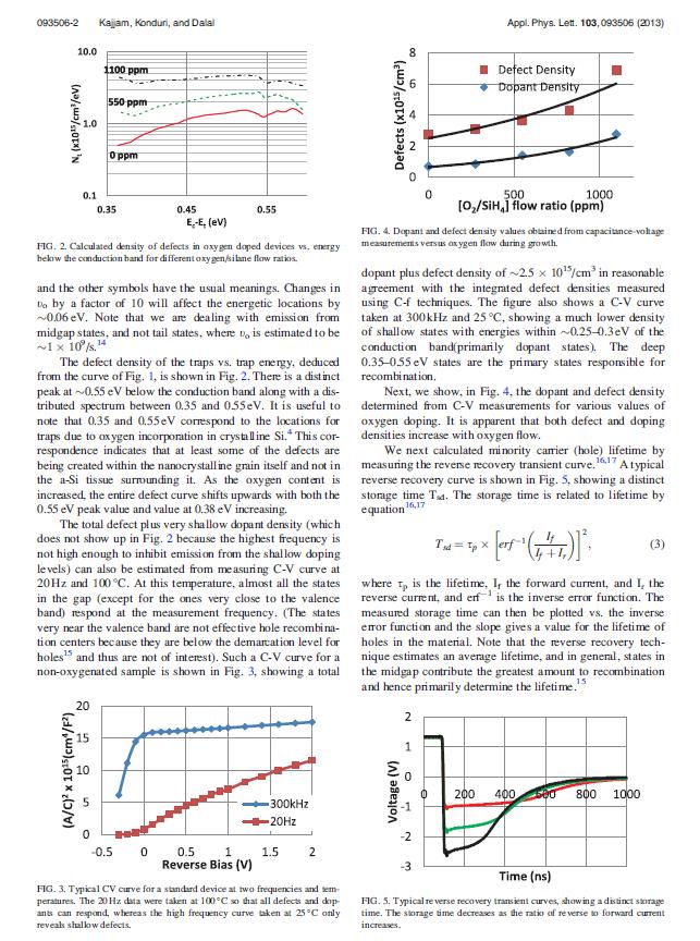
124 113
125 114
126 115 Defects and Doping in Nanocrystalline Silicon-Germanium Devices This work was published in MRS proceedings 2014 Siva Konduri, Watson Mulder and Vikram L. Dalal Department of Electrical and Computer Engineering, Iowa State University, Ames, Iowa ABSTRACT Nanocrystalline Silicon-Germanium (Si,Ge) is a potentially useful material for photovoltaic devices and photo-detectors. Its bandgap can be controlled across the entire bandgap region from that of Si to that of Ge by changing the alloy composition during growth. In this work, we study the fabrication and electronic properties of nanocrystalline devices grown using PECVD techniques. We discovered that upon adding Ge to Si during growth, the intrinsic layer changes from n-type to p-type. We can change it back to n-type by using ppm levels of phosphorus, and make reasonable quality devices when phosphine gas was added to the deposition mix. We also measured the defect density spectrum using capacitance frequency techniques, and find that defect density decreases systematically as more phosphine is added to the gas phase. We also find that the ratio of Germanium to Silicon in the solid phase is higher than the ratio in the gas phase. INTRODUCTION Nanocrystalline Si (nc-si) is an important and useful material for solar cells and photodetectors. Significant progress has been made in the solar conversion of efficiency of nc-si with efficiencies exceeding 10% in single junction cells, and exceeding 15% in multiple junction cells[1-5]. However, there has been little progress in increasing the efficiencies of
127 116 nanocrystalline (Si,Ge) alloys[6-10], which can potentially achieve high quantum efficiencies in the infrared range out to 0.68 ev i.e. the bandgap of crystalline Ge. It is usually found that as one adds Ge to Si, the device performance becomes worse, and it has been speculated that this decrease in performance is due to additional Ge-associated defects in the material [10, 11]. In this paper, we show that addition of Ge to Si leads to significant increases in defect density, and may even make the intrinsic n layer material to p-type. We also show that addition of ppm levels of phosphorus, using phosphine, to the intrinsic layer reduces the defect density and makes the material n type again, and allows one to achieve reasonable devices with quantum efficiencies extending further into the infrared regions. EXPERIMENTS The materials and devices were fabricated using PECVD techniques using a VHF plasma at ~47 MHz. The substrate temperature was in the range of ~250 C and pressure was ~ 100mT. The precursor gases were hydrogen, silane and 10% germane diluted in hydrogen. Varying levels of Ge:Si could be produced by varying the ratio of germane to silane flow ratio. Ppm levels of dopants such as phosphorus and boron could be introduced in the base (intrinsic) layer using dopants such as phosphine and diborane diluted in hydrogen. The devices were standard p+in+ devices, deposited on pre-cleaned stainless steel substrates with the i layer generally being n type for nc-si. ITO dots are deposited as top contacts and contact area is 0.12cm2. SiGe is used as p-layer to avoid kinks in bandgap and a smooth transition at p-i interface and Ge concentration in p-layer is around 20%. The basic device structure of nc- SiGe:H solar cell is shown in Fig. 1. Thickness of i-layer is about 0.70 μm.
![117 Figure 1. Typical device structure of nc-sige:h solar cell For measuring defect densities, we used the capacitance-frequency techniques described previously [12].](/docs-images/79/79335440/images/128-0.jpg "Device quantum efficiency (QE) was also measured using standard techniques. The ratio of Ge:Si in the solid phase was determined using energy dispersive x-ray spectroscopy. RESULTS In Fig.")
128 117 Figure 1. Typical device structure of nc-sige:h solar cell For measuring defect densities, we used the capacitance-frequency techniques described previously [12]. Device quantum efficiency (QE) was also measured using standard techniques. The ratio of Ge:Si in the solid phase was determined using energy dispersive x-ray spectroscopy. RESULTS In Fig. 2, we show the ratio of Ge:Si in the solid phase for various germane:silane flow rates. It is clear from this figure that much more Ge is incorporated in the solid phase as than is present in the gas phase. Figure 2. Germanium content for different gas flows in nc-sige:h devices
129 118 In Fig. 3a, we show the illuminated I-V curves for samples prepared using varying germane:silane ratios. A surprising result is that the short-circuit current actually decreases as the germane content in the gas phase increases. This is in spite of the fact that the germane:silane ratio in the solid phase is increasing, thereby implying a smaller bandgap material for higher germane flows. The explanation for this behavior is provided by studying quantum efficiency data, shown in Fig. 3b. It is clear from the QE data that there is a drastic reduction in QE for short wavelengths when significant amounts of germane is added to the input gas mixture. This can be ascribed to poor collection of electrons being generated near the p-n interface by light of shorter wavelengths, i.e. to a drastic reduction in electron diffusion length. This could be a result of the n-type intrinsic layer changing to a p-type, presumably due to Ge defects absorbing electrons from the oxygen induced donor states [13]. Indeed, there appears to be a significant increase in defect density when Ge content increases. See Fig. 4 for data on defect density vs. energy for varying German:Silane flow rates. Figure 3. (a) IV curves and (b) Absolute QE vs. Wavelength for nc-sige:h solar cells with varying Ge content

130 119 Figure 4. Calculated defect density vs. energy below the conduction band for varying Ge content To overcome the deleterious effects of additional Ge on both defect density and QE, we tried to compensate for the apparent p-type doping by adding ppm levels of PH3 to the gas mixture. The results for I-V curve are shown in Fig. 5a for various values of PH3 for a fixed germane:silane ratio of in the gas phase. Clearly, adding PH3 significantly improves the shortcircuit current in the solar cell. The corresponding QE curves are shown in Fig. 5b, and they clearly show an improvement in QE at short wavelengths, compared to the QE curves shown in Fig. 3, thus showing that the poor electron collection efficiency for photons which are absorbed near the p-intrinsic layer interface has been overcome. The corresponding change in total defect density as a function of PH3 flow is shown in Fig.6, thus confirming that addition of ppm levels of PH3 serves to reduce the defect density in nanocrystalline (Si,Ge) intrinsic layers, probably by compensating the defects caused by Ge addition.
131 120 Figure 5. (a) IV curves and (b) Absolute QE vs. Wavelength for nc-sige:h solar cells with (XGe~0.35) for varying PH3 flow rates Figure 6. Total defect density as a function of PH3 flow rate I-V curves for the devices prepared using varying ratios of germane:silane flow along with optimum ppm levels of PH3 are plotted in Fig.7a, which clearly shows that increasing Ge content leads to higher short-circuit currents but approximately the same open-circuit voltage. In general, Voc depends on quality of i-layer, type of p-layer and transition layers. Further experiments are being conducted to examine the relationship of Voc with Ge content. The
132 121 corresponding QE data in Fig. 7b shows that increasing Ge content shifts the curves to longer wavelengths, as expected. Figure 7. (a) IV curves and (b) Absolute QE vs. Wavelength for nc-sige:h solar cells with varying Ge content with optimum PH3 flow (i-layer Thickness ~ 0.7μm) CONCLUSIONS In conclusion, we have shown that the defect density in the intrinsic layer of nanocrystalline p-i-n solar cells material increases significantly as Ge content increases. It appears that adding Ge changes the doping type of the intrinsic layer form n-type to p-type. This shift leads to a drastic reduction in quantum efficiency for short wavelength photons at higher Ge concentrations. The defect density can be reduced, and the p-type behavior changed back to n-type by adding ppm levels of PH3 to the gas phase. The results show that when appropriate compensation by Phosphorus has been achieved, the quantum efficiency for solar cells extends further out towards longer wavelengths as the Ge content of the solar cell intrinsic layer increases, as expected, resulting in larger currents. This is an important result which shows that nanocrystalline (Si,Ge) cells can be used to improve the efficiency of tandem junction solar cells, as also the infrared response when these materials are used as photodetectors.
133 122 ACKNOWLEDGMENTS It is a pleasure to acknowledge the technical help of Andrew Gulstad and Max Noack. This work was partially supported by a grant from NSF. REFERENCES 1. J. Meier, R. Flückiger, H. Keppner and A. Shah, Applied Physics Letters, 65, (1994) 2. A. Shah, J. Meier, E. Vallat-Sauvain, C. Droz, U. Kroll, N. Wyrsch, J. Guillet and U. Graf, Thin Solid Films, , , (2002) 3. A. Shah, J. Meier, E. Vallat-Sauvain, N. Wyrsch, U. Kroll, C. Droz and U. Graf, Solar Energy Materials and Solar Cells, 78, , (2003) 4. V. Dalal, J. Leib, K. Muthukrisnan, D. Stieler, and M. Noack, 2005 IEEE Photovoltaic Specialists Conference, , (2005) 5. G. Yue, B. Yan, L. Sivec, T. Su, Y. Zhou, J. Yang and S. Guha, 2012 MRS Proceedings, 1426, 33-38, (2012) 6. M. Isomura, K. Nakahata, M. Shima, S. Taira, K. Wakisaka, M. Tanaka and S. Kiyama, Solar Energy Materials and Solar Cells, 74 (1 4), (2002) 7. J. K.Rath, F.D. Tichelaar and R. E.I Schropp, Solar energy materials and solar cells, 74, (2002) 8. S. Saripalli and V. Dalal, EIT 2008 IEEE International Conference Proceedings, , (2008) 9. T. Matsui, M. Kondo, K. Ogata, T. Ozawa and M. Isomura, Applied Physics Letters, 89, , (2006) 10. T. Matsui, K. Ogata, C.W. Chang, M. Isomura and M. Kondo, Journal of Non-Crystalline Solids, 354 (19 25), , (2008) 11. T. Matsui, C.W. Chang, T. Takada, M. Isomura, H. Fujiwara and M. Kondo, Solar Energy Materials and Solar Cells, 93, , (2009) 12. K. Shantan, K. Siva and V. Dalal, Applied Physics Letters, 103, (2013) 13. T. Matsui, C.W. Chang, K. Mizuno, Y. Takeuchi and M. Kondo, Japanese Journal of Applied Physics, 51, , (2012)
134 123 APPENDIX B Defect Density Profile of Perovskite Solar Cells Modified from paper submitted to Applied Physics Letters 2014 [11] Mehran Samiee, 1 Siva Konduri, 1 Balaji Ganapathy, 2 Ranjith Kottokkaran, 2 Hisham A. Abbas, 1 Andrew Kitahara, 3 Pranav Joshi, 1 Liang Zhang, 1 Max Noack, 2 and Vikram Dalal, 1 1 Dept. of Electrical and Computer Engineering, Iowa State University, Ames, IA Microelectronics Research Center, Iowa State University, Ames, Iowa 50011, USA 3 Dept. of Materials Science and Engineering, Iowa State University, Ames, Iowa 50011, USA ABSTRACT We report on measurement of dielectric constant, mid-gap defect density, Urbach energy of tail states in CH3NH3PbIXCl1-X perovskite solar cells. Midgap defect densities were estimated by measuring capacitance vs. frequency at different temperatures and show two peaks, one at 0.66 ev below the conduction band and one at 0.24 ev below the conduction band. The attempt to escape frequency is in the range of 2x10 11 /s. Quantum efficiency data indicate a bandgap of 1.58 ev. Urbach energies of valence and conduction band are estimated to be ~16 and ~18 mev. Measurement of saturation capacitance indicates that the relative dielectric constant is ~18.

135 124 INTRODUCTION In this section, Perovskite solar cells are briefly explained followed by detailed discussion on their defect density. Perovskite solar cells are exciting technology with conversion efficiencies exceeding 19% [1 6]. It is shown that, this material is poly-crystalline, high absorption coefficients with relatively small exciton binding energy [7] and diffusion lengths approaching 1 µm for both carriers [8]. For better understanding of device physics of Perovskite solar cells, it is important to study the defect density and spatial distribution of traps. EXPERIMENTAL DETAILS A typical Perovskite based solar cell device structure is shown in Figure 1. The n-i-p structure consists of TiO2/perovskite/p-heterojunction/gold structure. Compact layer of TiO2 is deposited on a FTO (Fluorine-doped Tin Oxide) substrate, followed by deposition of Lead Iodide (PbI2) and to form Perovksite, these PbI2 films were annealed in Methyl Ammonium Iodide (CH3NH3I) vapor at 150 C in N2 atmosphere [9]. The hole-transporting layer of P3HT (Poly-3-Hexyl Thiophene) was formed using spincoating, and finally 80 nm of Gold contacts were thermally evaporated. Figure 1. Device structure of Perovskite based solar cell
136 125 RESULTS JV characteristics and EQE curve are shown in Figure 2 with a power conversion efficiency of around 15% and Jsc of about 22mA/cm 2. The thickness of the i-layer is 460 nm and the bandgap of the material is 1.6 ev. Even with very high efficiencies and inherent carrier properties, Perovskite lags in stability. The main focus should be degradation studies as Perovskite is sensitive to moisture [10]. It is very important to study about the fundamental defects in Perovksite for better understating of device physics. Figure 2. (a) Illuminated JV curves measured using solar simulator and (b) QE vs. Wavelength for Pb-halide based Perovskite solar cells In Figure 3, the experimental data for CF and differential capacitance at various temperatures is plotted. In this material also, capacitance shift is observed at two distinctive bands. As the Perovskite is a higher bandgap material, temperature >300K is required to reach the midgap states. The inset in the Figure 3 exhibits that existence of secondary peak related to a trap level in addition to midgap defect state.
 Differential capacitance curves.")
137 126 Figure 3. (a) CF at various Temperatures for Perovksite based solar cell. The red arrows indicate the shift in capacitance. (b) Differential capacitance curves. Arrows indicate emission peaks.

138 127 Figure 4. Arrhenius plot of the differential capacitance peak frequencies vs. 1/kT for Perovkite solar cell The Arrhenius plot deduced from the differential capacitance curve of Figure 3 is shown in Figure 4, and the slope indicates trap energy levels at ~0.66 ev and ~0.24 ev below the conduction band. The ATE calculated from the intercept of dominant midgap trap is ~2x10 11 Hz. The defect density plot using CF data at room temperature (300K) is shown in Figure 5 and a major peak corresponding to midlevel trap is observed at around 0.65 ev below conduction band, with a peak value of 3x10 16 cm -3 ev -1. The defect density curve on a linear plot shown an excellent Gaussian fit and centered at ~0.65 ev, which is in agreement with the activation energy found in Arrhenius plot. Table 1 summarizes the averaged parameters derived from CFT data. Table 1. Summary of the averaged parameters from CFT data of Perovskite solar cell Activation Energy, Ea 260 mev 680 mev ATE, ν0 6x10 8 Hz 2 x10 11 Hz Pre-factor, ϒ 6.7x10 3 Hz K x10 6 Hz K -2 Capture cross-section, σn * 6x10-18 cm 2 2 x10-14 cm 2
Amorphous Silicon Solar Cells
 The Birnie Group solar class and website were created with much-appreciated support from the NSF CRCD Program under grants 0203504 and 0509886. Continuing Support from the McLaren Endowment is also greatly
Materials, Electronics and Renewable Energy
 Materials, Electronics and Renewable Energy Neil Greenham ncg11@cam.ac.uk Inorganic semiconductor solar cells Current-Voltage characteristic for photovoltaic semiconductor electrodes light Must specify
Thin film silicon technology. Cosimo Gerardi 3SUN R&D Tech. Coordinator
 Thin film silicon technology Cosimo Gerardi 3SUN R&D Tech. Coordinator 1 Outline Why thin film Si? Advantages of Si thin film Si thin film vs. other thin film Hydrogenated amorphous silicon Energy gap
Preparation and Characterization of Micro-Crystalline Hydrogenated Silicon Carbide p-layers
 Preparation and Characterization of Micro-Crystalline Hydrogenated Silicon Carbide p-layers Erten Eser, Steven S. Hegedus and Wayne A. Buchanan Institute of Energy Conversion University of Delaware, Newark,
Available online at ScienceDirect. Energy Procedia 84 (2015 ) 17 24
 17 24") Available online at www.sciencedirect.com ScienceDirect Energy Procedia 84 (2015 ) 17 24 E-MRS Spring Meeting 2015 Symposium C - Advanced inorganic materials and structures for photovoltaics Annealing
Available online at www.sciencedirect.com ScienceDirect Energy Procedia 84 (2015 ) 17 24 E-MRS Spring Meeting 2015 Symposium C - Advanced inorganic materials and structures for photovoltaics Annealing
Properties of Amorphous Silicon Germanium Films and Devices Prepared Using Chemical Annealing
 Graduate Theses and Dissertations Graduate College 2013 Properties of Amorphous Silicon Germanium Films and Devices Prepared Using Chemical Annealing Zhao Li Iowa State University Follow this and additional
Study of a-sige:h Films and n-i-p Devices used in High Efficiency Triple Junction Solar Cells.
 Study of a-sige:h Films and n-i-p Devices used in High Efficiency Triple Junction Solar Cells. Pratima Agarwal*, H. Povolny, S. Han and X. Deng. Department of Physics and Astronomy, University of Toledo,
OPTICAL, ELECTRICAL AND STRUCTURAL PROPERTIES OF PECVD QUASI EPITAXIAL PHOSPHOROUS DOPED SILICON FILMS ON CRYSTALLINE SILICON SUBSTRATE
 OPTICAL, ELECTRICAL AN STRUCTURAL PROPERTIES OF PECV QUASI EPITAXIAL PHOSPHOROUS OPE SILICON FILMS ON CRYSTALLINE SILICON SUBSTRATE Mahdi Farrokh-Baroughi, Hassan El-Gohary, and Siva Sivoththaman epartment
Silver Diffusion Bonding and Layer Transfer of Lithium Niobate to Silicon
 Chapter 5 Silver Diffusion Bonding and Layer Transfer of Lithium Niobate to Silicon 5.1 Introduction In this chapter, we discuss a method of metallic bonding between two deposited silver layers. A diffusion
PLASMA ENHANCED CHEMICAL VAPOR DEPOSITION OF SILICON THIN FILMS: CHARACTERIZATION OF FILM GROWTH
 PLASMA ENHANCED CHEMICAL VAPOR DEPOSITION OF SILICON THIN FILMS: CHARACTERIZATION OF FILM GROWTH AT DIFFERENT FREQUENCIES AND GAS COMPOSITIONS UTILIZING PLASMA DIAGNOSTICS by Lala Zhu A dissertation submitted
Basics of Solar Photovoltaics. Photovoltaics (PV) Lecture-21
 Lecture-21") Lecture-21 Basics of Solar Photovoltaics Photovoltaics (PV) Photovoltaics (PV) comprise the technology to convert sunlight directly into electricity. The term photo means light and voltaic, electricity.
Lecture-21 Basics of Solar Photovoltaics Photovoltaics (PV) Photovoltaics (PV) comprise the technology to convert sunlight directly into electricity. The term photo means light and voltaic, electricity.
I. GaAs Material Properties
 I. GaAs Material Properties S. Kayali GaAs is a III V compound semiconductor composed of the element gallium (Ga) from column III and the element arsenic (As) from column V of the periodic table of the
1. Introduction. What is implantation? Advantages
 Ion implantation Contents 1. Introduction 2. Ion range 3. implantation profiles 4. ion channeling 5. ion implantation-induced damage 6. annealing behavior of the damage 7. process consideration 8. comparison
Halbleiter Prof. Yong Lei Prof. Thomas Hannappel
 Halbleiter Prof. Yong Lei Prof. Thomas Hannappel yong.lei@tu-ilmenau.de thomas.hannappel@tu-ilmenau.de http://www.tu-ilmenau.de/nanostruk/ Solid State Structure of Semiconductor Semiconductor manufacturing
Production of PV cells
 Production of PV cells MWp 1400 1200 Average market growth 1981-2003: 32% 2004: 67% 1000 800 600 400 200 0 1991 1992 1993 1994 1995 1996 1997 1998 1999 2000 2001 2002 2003 2004 rest 1.0 1.0 1.0 2.0 4.0
Grid-Tied PV System with Energy Optimization
 International Journal of Engineering Works Kambohwell Publisher Enterprises Vol. 4, Issue 10, PP. 184-189, October 2017 www.kwpublisher.com Grid-Tied PV System with Energy Optimization Maryam Shahjehan,
Topics Relevant to CdTe Thin Film Solar Cells
 Topics Relevant to CdTe Thin Film Solar Cells March 13, 2012 The University of Toledo, Department of Physics and Astronomy SSARE, PVIC Principles and Varieties of Solar Energy (PHYS 4400) and Fundamentals
Recap of a-si and a-si cell technology Types of a-si manufacturing systems a-si cell and module manufacturing at Xunlight. Xunlight Corporation
 Thin-Film Silicon Technology and Manufacturing Recap of a-si and a-si cell technology Types of a-si manufacturing systems a-si cell and module manufacturing at Xunlight Xunlight products and installations
Hsin-Ying Lee, 1 Ting-Chun Wang, 1 and Chun-Yen Tseng Introduction
 International Photoenergy, Article ID 795152, 5 pages http://dx.doi.org/10.1155/2014/795152 Research Article Performance Improvement of Microcrystalline p-sic/i-si/n-si Thin Film Solar Cells by Using Laser-Assisted
Characterization of Polycrystalline SiC Films Grown by HW-CVD using Silicon Tetrafluoride
 Characterization of Polycrystalline SiC Films Grown by HW-CVD using Silicon Tetrafluoride Katsuya Abe, Yohei Nagasaka, Takahiro Kida, Tomohiko Yamakami, Rinpei Hayashibe and Kiichi Kamimura, Faculty of
SUPPLEMENTARY INFORMATION
 In the format provided by the authors and unedited. ARTICLE NUMBER: 16178 DOI: 10.1038/NENERGY.2016.178 Enhanced Stability and Efficiency in Hole-Transport Layer Free CsSnI3 Perovskite Photovoltaics Supplementary
Hei Wong.
 Defects and Disorders in Hafnium Oxide and at Hafnium Oxide/Silicon Interface Hei Wong City University of Hong Kong Email: heiwong@ieee.org Tokyo MQ2012 1 Outline 1. Introduction, disorders and defects
Solar Spectrum. -Black body radiation. Light bulb 3000 K Red->Yellow->White Surface of Sun 6000 K
 Solar Spectrum 1 Solar Spectrum -Black body radiation Light bulb 3000 K Red->Yellow->White Surface of Sun 6000 K 2 Solar Spectrum -Black body radiation Light bulb 3000 K Red->Yellow->White Surface of Sun
Improving the stability of amorphous silicon solar cells by chemical annealing
 Retrospective Theses and Dissertations 2006 Improving the stability of amorphous silicon solar cells by chemical annealing Nanlin Wang Iowa State University Follow this and additional works at: http://lib.dr.iastate.edu/rtd
FABRICATION ENGINEERING MICRO- NANOSCALE ATTHE AND. Fourth Edition STEPHEN A. CAMPBELL. of Minnesota. University OXFORD UNIVERSITY PRESS
 AND FABRICATION ENGINEERING ATTHE MICRO- NANOSCALE Fourth Edition STEPHEN A. CAMPBELL University of Minnesota New York Oxford OXFORD UNIVERSITY PRESS CONTENTS Preface xiii prrt i OVERVIEW AND MATERIALS
Growth and properties of (ultra) nano crystalline diamond
 nano crystalline diamond") Growth and properties of (ultra) nano crystalline diamond Hadwig Sternschulte 1,2 1 nanotum, Technische Universität München, D-85748 Garching, Germany 2 Physik Department E19, Technische Universität München,
Growth and properties of (ultra) nano crystalline diamond Hadwig Sternschulte 1,2 1 nanotum, Technische Universität München, D-85748 Garching, Germany 2 Physik Department E19, Technische Universität München,
Growth and Doping of SiC-Thin Films on Low-Stress, Amorphous Si 3 N 4 /Si Substrates for Robust Microelectromechanical Systems Applications
 Journal of ELECTRONIC MATERIALS, Vol. 31, No. 5, 2002 Special Issue Paper Growth and Doping of SiC-Thin Films on Low-Stress, Amorphous Si 3 N 4 /Si Substrates for Robust Microelectromechanical Systems
HOMEWORK 4 and 5. March 15, Homework is due on Monday March 30, 2009 in Class. Answer the following questions from the Course Textbook:
 HOMEWORK 4 and 5 March 15, 2009 Homework is due on Monday March 30, 2009 in Class. Chapter 7 Answer the following questions from the Course Textbook: 7.2, 7.3, 7.4, 7.5, 7.6*, 7.7, 7.9*, 7.10*, 7.16, 7.17*,
RightCopyright 2006 American Vacuum Soci
 Title Gallium nitride thin films deposite magnetron sputtering Author(s) Maruyama, T; Miyake, H Citation JOURNAL OF VACUUM SCIENCE & (2006), 24(4): 1096-1099 TECHNOL Issue Date 2006 URL http://hdl.handle.net/2433/43541
Materials Characterization
 Materials Characterization C. R. Abernathy, B. Gila, K. Jones Cathodoluminescence (CL) system FEI Nova NanoSEM (FEG source) with: EDAX Apollo silicon drift detector (TE cooled) Gatan MonoCL3+ FEI SEM arrived
Performance and Radiation Resistance of Quantum Dot Multi-Junction Solar Cells
 B.C. Richards 1, Young Lin 1, Pravin Patel 1, Daniel Chumney 1, Paul R. Sharps 1 Chris Kerestes 1,2, David Forbes 2, Kristina Driscoll 2, Adam Podell 2, Seth Hubbard 2 1 EMCORE Corporation, Albuquerque,
Fabrication Technology
 Fabrication Technology By B.G.Balagangadhar Department of Electronics and Communication Ghousia College of Engineering, Ramanagaram 1 OUTLINE Introduction Why Silicon The purity of Silicon Czochralski
Chapter 5 Epitaxial Growth of Si 1-y C y Alloys
 Chapter 5 Epitaxial Growth of Si 1-y C y Alloys 5.1 Introduction Traditionally, the incorporation of substitutional carbon into silicon and silicongermanium alloys during growth is of great interest for
Project III. 4: THIN FILM DEVICES FOR LARGE AREA ELECTRONICS
 Project III. 4: THIN FILM DEVICES FOR LARGE AREA ELECTRONICS Project leader: Dr D.N. Kouvatsos Collaborating researchers from other projects: Dr D. Davazoglou Ph.D. candidates: M. Exarchos, L. Michalas
Light-Induced Degradation of Thin Film Silicon Solar Cells
 Journal of Physics: Conference Series PAPER OPEN ACCESS Light-Induced Degradation of Thin Film Silicon Solar Cells To cite this article: F U Hamelmann et al 2016 J. Phys.: Conf. Ser. 682 012002 View the
Evaluating thermal imaging for identification and characterization of solar cell defects
 Graduate Theses and Dissertations Graduate College 2014 Evaluating thermal imaging for identification and characterization of solar cell defects Jiahao Chen Iowa State University Follow this and additional
Polycrystalline CdS/CdTe solar cells
 Polycrystalline CdS/CdTe solar cells Al Compaan Distinguished University Professor of Physics, Emeritus (Lecture for Heben/Ellingson solar cells class) March 3, 2011 1 Absorption spectra of various semiconductors
Lecture 12. Physical Vapor Deposition: Evaporation and Sputtering Reading: Chapter 12. ECE Dr. Alan Doolittle
 Lecture 12 Physical Vapor Deposition: Evaporation and Sputtering Reading: Chapter 12 Evaporation and Sputtering (Metalization) Evaporation For all devices, there is a need to go from semiconductor to metal.
An Evaluation of Solar Photovoltaic Technologies
 An Evaluation of Solar Photovoltaic Technologies 15.965 Technology Strategy Paper 1, February 23, 2009 Introduction: Green thinking is the in topic these days. Companies are all claiming to be going green.
Growth Of TiO 2 Films By RF Magnetron Sputtering Studies On The Structural And Optical Properties
 Journal of Multidisciplinary Engineering Science and Technology (JMEST) Growth Of TiO 2 Films By RF Magnetron Sputtering Studies On The Structural And Optical Properties Ahmed K. Abbas 1, Mohammed K. Khalaf
State of the art quality of a GeOx interfacial passivation layer formed on Ge(001)
") APPLICATION NOTE State of the art quality of a Ox interfacial passivation layer formed on (001) Summary A number of research efforts have been made to realize Metal-Oxide-Semiconductor Field Effect Transistors
APPLICATION NOTE State of the art quality of a Ox interfacial passivation layer formed on (001) Summary A number of research efforts have been made to realize Metal-Oxide-Semiconductor Field Effect Transistors
Organic Solar Cells. Green River Project
 Organic Solar Cells Green River Project Silicon Cells Silicon semiconductors Advantages: Efficiencies Lifetimes Disadvantages: High manufacturing costs Inflexible http://en.wikipedia.org Organic semiconductors
Yung-Hui Yeh, and Bo-Cheng Kung Display Technology Center (DTC), Industrial Technology Research Institute, Hsinchu 310, Taiwan
, Industrial Technology Research Institute, Hsinchu 310, Taiwan") Amorphous In 2 O 3 -Ga 2 O 3 -ZnO Thin Film Transistors and Integrated Circuits on Flexible and Colorless Polyimide Substrates Hsing-Hung Hsieh, and Chung-Chih Wu* Graduate Institute of Electronics Engineering,
Amorphous In 2 O 3 -Ga 2 O 3 -ZnO Thin Film Transistors and Integrated Circuits on Flexible and Colorless Polyimide Substrates Hsing-Hung Hsieh, and Chung-Chih Wu* Graduate Institute of Electronics Engineering,
Activation Behavior of Boron and Phosphorus Atoms Implanted in Polycrystalline Silicon Films by Heat Treatment at 250 C
 Japanese Journal of Applied Physics Vol. 44, No. 3, 2005, pp. 1186 1191 #2005 The Japan Society of Applied Physics Activation Behavior of Boron and Phosphorus Atoms Implanted in Polycrystalline Silicon
VLSI INTRODUCTION P.VIDYA SAGAR ( ASSOCIATE PROFESSOR) Department of Electronics and Communication Engineering, VBIT
 Department of Electronics and Communication Engineering, VBIT") VLSI INTRODUCTION P.VIDYA SAGAR ( ASSOCIATE PROFESSOR) contents UNIT I INTRODUCTION: Introduction to IC Technology MOS, PMOS, NMOS, CMOS & BiCMOS technologies. BASIC ELECTRICAL PROPERTIES : Basic Electrical
VLSI INTRODUCTION P.VIDYA SAGAR ( ASSOCIATE PROFESSOR) contents UNIT I INTRODUCTION: Introduction to IC Technology MOS, PMOS, NMOS, CMOS & BiCMOS technologies. BASIC ELECTRICAL PROPERTIES : Basic Electrical
Figure 2.3 (cont., p. 60) (e) Block diagram of Pentium 4 processor with 42 million transistors (2000). [Courtesy Intel Corporation.
 (e) Block diagram of Pentium 4 processor with 42 million transistors (2000). [Courtesy Intel Corporation.") Figure 2.1 (p. 58) Basic fabrication steps in the silicon planar process: (a) oxide formation, (b) selective oxide removal, (c) deposition of dopant atoms on wafer, (d) diffusion of dopant atoms into exposed
Figure 2.1 (p. 58) Basic fabrication steps in the silicon planar process: (a) oxide formation, (b) selective oxide removal, (c) deposition of dopant atoms on wafer, (d) diffusion of dopant atoms into exposed
Chapter 3 Silicon Device Fabrication Technology
 Chapter 3 Silicon Device Fabrication Technology Over 10 15 transistors (or 100,000 for every person in the world) are manufactured every year. VLSI (Very Large Scale Integration) ULSI (Ultra Large Scale
"Plasma CVD passivation; Key to high efficiency silicon solar cells",
 "Plasma CVD passivation; Key to high efficiency silicon solar cells", David Tanner Date: May 7, 2015 2012 GTAT Corporation. All rights reserved. Summary: Remarkable efficiency improvements of silicon solar
Correlation Between Energy Gap and Defect Formation of Al Doped Zinc Oxide on Carbon Doped Silicon Oxide
 TRANSACTIONS ON ELECTRICAL AND ELECTRONIC MATERIALS Vol. 15, No. 4, pp. 207-212, August 25, 2014 Regular Paper pissn: 1229-7607 eissn: 2092-7592 DOI: http://dx.doi.org/10.4313/teem.2014.15.4.207 Correlation
Lecture 8. Deposition of dielectrics and metal gate stacks (CVD, ALD)
") Lecture 8 Deposition of dielectrics and metal gate stacks (CVD, ALD) Thin Film Deposition Requirements Many films, made of many different materials are deposited during a standard CMS process. Gate Electrodes
Lecture 8 Deposition of dielectrics and metal gate stacks (CVD, ALD) Thin Film Deposition Requirements Many films, made of many different materials are deposited during a standard CMS process. Gate Electrodes
PECVD deposition of a-si:h and µc-si:h using a linear RF source
 PECVD deposition of a-si:h and µc-si:h using a linear RF source Bas B. Van Aken *, Camile Devilee, Maarten Dörenkämper, Marco Geusebroek, Maurits Heijna, Jochen Löffler, Wim J. Soppe ECN Solar Energy,
Metallization deposition and etching. Material mainly taken from Campbell, UCCS
 Metallization deposition and etching Material mainly taken from Campbell, UCCS Application Metallization is back-end processing Metals used are aluminum and copper Mainly involves deposition and etching,
Optics and Photovoltaics Physics 9810b Course Information: Winter 2012
 The University of Western Ontario Department of Physics and Astronomy Optics and Photovoltaics Physics 9810b Course Information: Winter 2012 1. Course Description Objective of this course is to provide
Transmission Mode Photocathodes Covering the Spectral Range
 Transmission Mode Photocathodes Covering the Spectral Range 6/19/2002 New Developments in Photodetection 3 rd Beaune Conference June 17-21, 2002 Arlynn Smith, Keith Passmore, Roger Sillmon, Rudy Benz ITT
Lecture 4. Oxidation (applies to Si and SiC only) Reading: Chapter 4
 Reading: Chapter 4") Lecture 4 Oxidation (applies to Si and SiC only) Reading: Chapter 4 Introduction discussion: Oxidation: Si (and SiC) Only The ability to grow a high quality thermal oxide has propelled Si into the forefront
Lecture 4 Oxidation (applies to Si and SiC only) Reading: Chapter 4 Introduction discussion: Oxidation: Si (and SiC) Only The ability to grow a high quality thermal oxide has propelled Si into the forefront
Ajay Kumar Gautam [VLSI TECHNOLOGY] VLSI Technology for 3RD Year ECE/EEE Uttarakhand Technical University
![Ajay Kumar Gautam [VLSI TECHNOLOGY] VLSI Technology for 3RD Year ECE/EEE Uttarakhand Technical University](/thumbs/75/72824557.jpg "Ajay Kumar Gautam [VLSI TECHNOLOGY] VLSI Technology for 3RD Year ECE/EEE Uttarakhand Technical University") 2014 Ajay Kumar Gautam [VLSI TECHNOLOGY] VLSI Technology for 3RD Year ECE/EEE Uttarakhand Technical University Page1 Syllabus UNIT 1 Introduction to VLSI Technology: Classification of ICs, Scale of integration,
2014 Ajay Kumar Gautam [VLSI TECHNOLOGY] VLSI Technology for 3RD Year ECE/EEE Uttarakhand Technical University Page1 Syllabus UNIT 1 Introduction to VLSI Technology: Classification of ICs, Scale of integration,
Schottky Tunnel Contacts for Efficient Coupling of Photovoltaics and Catalysts
 Schottky Tunnel Contacts for Efficient Coupling of Photovoltaics and Catalysts Christopher E. D. Chidsey Department of Chemistry Stanford University Collaborators: Paul C. McIntyre, Y.W. Chen, J.D. Prange,
Passivation of silicon wafers by Silicon Carbide (SiC x ) thin film grown by sputtering
 thin film grown by sputtering") Available online at www.sciencedirect.com Energy Procedia 10 (2011 ) 71 75 European Materials Research Society Conference Symp. Advanced Inorganic Materials and Concepts for Photovoltaics Passivation of
Available online at www.sciencedirect.com Energy Procedia 10 (2011 ) 71 75 European Materials Research Society Conference Symp. Advanced Inorganic Materials and Concepts for Photovoltaics Passivation of
Microstructure-Properties: I Lecture 5B The Effect of Grain Size. on Varistors
 1 Microstructure-Properties: I Lecture 5B The Effect of on 27-301 October, 2007 A. D. Rollett 2 This lecture is concerned with the effects of grain size on properties. This is the second of two examples:
EECS130 Integrated Circuit Devices
 EECS130 Integrated Circuit Devices Professor Ali Javey 9/13/2007 Fabrication Technology Lecture 1 Silicon Device Fabrication Technology Over 10 15 transistors (or 100,000 for every person in the world)
The growth of patterned ceramic thin films from polymer precursor solutions Göbel, Ole
 University of Groningen The growth of patterned ceramic thin films from polymer precursor solutions Göbel, Ole IMPORTANT NOTE: You are advised to consult the publisher's version (publisher's PDF) if you
Thin film photovoltaics: industrial strategies for increasing the efficiency and reducing costs
 STATO E PROSPETTIVE DEL FOTOVOLTAICO IN ITALIA 26 giugno 2014 ENEA Via Giulio Romano n. 41, Roma Thin film photovoltaics: industrial strategies for increasing the efficiency and reducing costs Anna Battaglia,
Mn DOPED SnO2 Semiconducting Magnetic Thin Films Prepared by Spray Pyrolysis Method
 International Journal of Scientific & Engineering Research Volume 2, Issue 4, April-2011 1 Mn DOPED SnO2 Semiconducting Magnetic Thin Films Prepared by Spray Pyrolysis Method K.Vadivel, V.Arivazhagan,
Thermal Evaporation. Theory
 Thermal Evaporation Theory 1. Introduction Procedures for depositing films are a very important set of processes since all of the layers above the surface of the wafer must be deposited. We can classify
Defense Technical Information Center Compilation Part Notice
 UNCLASSIFIED Defense Technical Information Center Compilation Part Notice ADP012232 TITLE: Microwave Plasma CVD of Silicon Nanocrystalline and Amorphous Silicon as a Function of Deposition Conditions DISTRIBUTION:
Amorphous silicon waveguides for microphotonics
 4 Amorphous silicon waveguides for microphotonics Amorphous silicon a-si was made by ion irradiation of crystalline silicon with 1 10 15 Xe ions cm 2 at 77 K in the 1 4 MeV energy range. Thermal relaxation
Excimer Laser Annealing of Hydrogen Modulation Doped a-si Film
 Materials Transactions, Vol. 48, No. 5 (27) pp. 975 to 979 #27 The Japan Institute of Metals Excimer Laser Annealing of Hydrogen Modulation Doped a-si Film Akira Heya 1, Naoto Matsuo 1, Tadashi Serikawa
The Effects of the Adding V2O5 on the Oxide Semiconductor Layer of a Dye-sensitized Solar Cell
 , pp.66-71 http://dx.doi.org/10.14257/astl.2016.140.14 The Effects of the Adding V2O5 on the Oxide Semiconductor Layer of a Dye-sensitized Solar Cell Don-Kyu Lee Electrical Engineering, Dong-Eui University,
Supporting Online Material for
 www.sciencemag.org/cgi/content/full/science.1200448/dc1 Supporting Online Material for Increasing Solar Absorption for Photocatalysis with Black Hydrogenated Titanium Dioxide Nanocrystals This PDF file
X ray diffraction in materials science
 X ray diffraction in materials science Goals: Use XRD spectra to determine the orientation of single crystals and preferred orientations in a thin film. Understand how grain size and strain affect the
Thin film PV Technologies Thin film Silicon PV Technology
 Thin film PV Technologies Thin film Silicon PV Technology Week 5.2 Arno Smets Thin film Silicon solar cell Semiconductor Materials IV semiconductors: Si, Ge Rn Xe Kr Ar Ne He At I Br Cl F Po Te Se S O
Available online at ScienceDirect. Energy Procedia 92 (2016 ) Mathieu Boccard*, Nathan Rodkey, Zachary C.
 Mathieu Boccard*, Nathan Rodkey, Zachary C.") Available online at www.sciencedirect.com ScienceDirect Energy Procedia 92 (2016 ) 297 303 6th International Conference on Silicon Photovoltaics, SiliconPV 2016 High-mobility hydrogenated indium oxide
Available online at www.sciencedirect.com ScienceDirect Energy Procedia 92 (2016 ) 297 303 6th International Conference on Silicon Photovoltaics, SiliconPV 2016 High-mobility hydrogenated indium oxide
Introduction to Solar Cell Materials-I
 Introduction to Solar Cell Materials-I 23 July 2012 P.Ravindran, Elective course on Solar Rnergy and its Applications Auguest 2012 Introduction to Solar Cell Materials-I Photovoltaic cell: short history
Efficiency of Solar Cell Design and Materials
 S&T s Peer to Peer Volume 1 Issue 2 Article 7 May 2017 Efficiency of Solar Cell Design and Materials Grant VonderHaar Follow this and additional works at: http://scholarsmine.mst.edu/peer2peer Part of
Stable Hydrogenated Amorphous Silicon Germanium for Photovoltaic Applications. Experimental and Computational Studies.
 Stable Hydrogenated Amorphous Silicon Germanium for Photovoltaic Applications. Experimental and Computational Studies. Stable Hydrogenated Amorphous Silicon Germanium for Photovoltaic Applications. Experimental
TWO-DIMENSIONAL MODELING OF EWT MULTICRYSTALLINE SILICON SOLAR CELLS AND COMPARISON WITH THE IBC SOLAR CELL
 TWO-DIMENSIONAL MODELING OF EWT MULTICRYSTALLINE SILICON SOLAR CELLS AND COMPARISON WITH THE IBC SOLAR CELL Mohamed M. Hilali, Peter Hacke, and James M. Gee Advent Solar, Inc. 8 Bradbury Drive S.E, Suite,
Semiconductor Very Basics
 Semiconductor Very Basics Material (mostly) from Semiconductor Devices, Physics & Technology, S.M. Sze, John Wiley & Sons Semiconductor Detectors, H. Spieler (notes) July 3, 2003 Conductors, Semi-Conductors,
Structurally integrated luminescence based oxygen sensors with Organic LED/ oxygen sensitive dye and PECVD grown thin film photodetectors
 Retrospective Theses and Dissertations 2008 Structurally integrated luminescence based oxygen sensors with Organic LED/ oxygen sensitive dye and PECVD grown thin film photodetectors Debju Ghosh Iowa State
Thin film CdS/CdTe solar cells: Research perspectives
 Solar Energy 80 (2006) 675 681 www.elsevier.com/locate/solener Thin film CdS/CdTe solar cells: Research perspectives Arturo Morales-Acevedo * CINVESTAV del IPN, Department of Electrical Engineering, Avenida
Solar Cells and Photosensors.
 Designing Photonic Crystals in Strongly Absorbing Material for Applications in Solar Cells and Photosensors. Minda Wagenmaker 1, Ebuka S. Arinze 2, Botong Qiu 2, Susanna M. Thon 2 1 Mechanical Engineering
High Quality a-ge:h Films and Devices Through Enhanced Plasma Chemistry
 Mater. Res. Soc. Symp. Proc. Vol. 989 2007 Materials Research Society 0989-A04-04 High Quality a-ge:h Films and Devices Through Enhanced Plasma Chemistry Erik V. Johnson, and Pere Roca i Cabarrocas LPICM
Nanosilicon single-electron transistors and memory
 Nanosilicon single-electron transistors and memory Z. A. K. Durrani (1, 2) and H. Ahmed (3) (1) Electronic Devices and Materials Group, Engineering Department, University of Cambridge, Trumpington Street,
and Technology of Thin Films
 An Introduction to Physics and Technology of Thin Films This page is intentionally left blank An Introduction to Physics and Technology of Thin Films Alfred Wagendriste1 Institute of Applied and Technical
Advanced Gate Stack, Source/Drain, and Channel Engineering for Si-Based CMOS 6: New Materials, Processes, and Equipment
 Advanced Gate Stack, Source/Drain, and Channel Engineering for Si-Based CMOS 6: New Materials, Processes, and Equipment Editors: E. P. Gusev Qualcomm MEMS Technologies San Jose, California, USA D-L. Kwong
Semiconductor Technology
 Semiconductor Technology from A to Z Oxidation www.halbleiter.org Contents Contents List of Figures List of Tables II III 1 Oxidation 1 1.1 Overview..................................... 1 1.1.1 Application...............................
Applications of Successive Ionic Layer Adsorption and Reaction (SILAR) Technique for CZTS Thin Film Solar Cells
 Technique for CZTS Thin Film Solar Cells") NANO VISION An International Open Free Access, Peer Reviewed Research Journal www.nano-journal.org ISSN 2231-2579 (Print) ISSN 2319-7633 (Online) Abbr: Nano Vision. 2013, Vol.3(3): Pg.235-239 Applications
NANO VISION An International Open Free Access, Peer Reviewed Research Journal www.nano-journal.org ISSN 2231-2579 (Print) ISSN 2319-7633 (Online) Abbr: Nano Vision. 2013, Vol.3(3): Pg.235-239 Applications
Structure and optical properties of M/ZnO (M=Au, Cu, Pt) nanocomposites
 nanocomposites") Solar Energy Materials & Solar Cells 8 () 339 38 Structure and optical properties of M/ (M=Au, Cu, Pt) nanocomposites U. Pal a,b, *, J. Garc!ıa-Serrano a, G. Casarrubias-Segura a, N. Koshizaki c, T. Sasaki
Solar Energy Materials & Solar Cells 8 () 339 38 Structure and optical properties of M/ (M=Au, Cu, Pt) nanocomposites U. Pal a,b, *, J. Garc!ıa-Serrano a, G. Casarrubias-Segura a, N. Koshizaki c, T. Sasaki
Impurity Photovoltaic Effect in Multijunction Solar Cells
 Available online at www.sciencedirect.com Procedia Technology 7 ( 2013 ) 166 172 The 2013 Iberoamerican Conference on Electronics Engineering and Computer Science Impurity Photovoltaic Effect in Multijunction
POLYMORPHOUS SILICON: TRANSPORT PROPERTIES AND SOLAR CELL APPLICATIONS
 POLYMORPHOUS SILICON: TRANSPORT PROPERTIES AND SOLAR CELL APPLICATIONS C. Longeaud*, J. P. Kleider*, M. Gauthier*, R. Brtiggemann*, Y. Poissant**, and P. Roca i Cabarrocas** * Laboratoire de Genie Electrique
Chapter 18: Electrical Properties
 Chapter 18: Electrical Properties ISSUES TO ADDRESS... How are electrical conductance and resistance characterized? What are the physical phenomena that distinguish conductors, semiconductors, and insulators?
Effect of nanoimprinted surface relief on Si and Ge nucleation and ordering
 Microelectronics Journal 37 (2006) 1481 1485 www.elsevier.com/locate/mejo Effect of nanoimprinted surface relief on Si and Ge nucleation and ordering T.I. Kamins a,, A.A. Yasseri a,1, S. Sharma a,2, R.F.W.
ZnO-based Transparent Conductive Oxide Thin Films
 IEEE EDS Mini-colloquium WIMNACT 32 ZnO-based Transparent Conductive Oxide Thin Films Weijie SONG Ningbo Institute of Material Technology and Engineering, Chinese Academy of Sciences, Ningbo, P. R. China
Characterization of cadmium zinc telluride solar cells
 University of South Florida Scholar Commons Graduate Theses and Dissertations Graduate School 2003 Characterization of cadmium zinc telluride solar cells Gowri Sivaraman University of South Florida Follow
A STUDY OF THE STAEBLER-WRONSKI EFFECT AND AMORPHOUS SILICON SOLAR CELLS
 A STUDY OF THE STAEBLER-WRONSKI EFFECT AND AMORPHOUS SILICON SOLAR CELLS By Kim SOLESVIK OPPEDAL MSc Candidate June 2013 Examination Committee: Prof. dr. M. Zeman Dr. ir. J.F. Creemer Dr. R.A.C.M.M. van
Formation and Annihilation of Hydrogen-Related Donor States in Proton-Implanted and Subsequently Plasma-Hydrogenated N-Type Float-Zone Silicon
 Formation and Annihilation of Hydrogen-Related Donor States in Proton-Implanted and Subsequently Plasma-Hydrogenated N-Type Float-Zone Silicon Reinhart Job, University of Hagen, Germany Franz-Josef Niedernostheide,
ME 141B: The MEMS Class Introduction to MEMS and MEMS Design. Sumita Pennathur UCSB
 ME 141B: The MEMS Class Introduction to MEMS and MEMS Design Sumita Pennathur UCSB Outline today Introduction to thin films Oxidation Deal-grove model CVD Epitaxy Electrodeposition 10/6/10 2/45 Creating
Lecture 22: Integrated circuit fabrication
 Lecture 22: Integrated circuit fabrication Contents 1 Introduction 1 2 Layering 4 3 Patterning 7 4 Doping 8 4.1 Thermal diffusion......................... 10 4.2 Ion implantation.........................
Fabrication of ultra thin CdS/CdTe solar cells by magnetron sputtering
 The University of Toledo The University of Toledo Digital Repository Theses and Dissertations 29 Fabrication of ultra thin CdS/CdTe solar cells by magnetron sputtering Victor Plotnikov The University of
IN-SITU ANNEALING OF Cu(In,Ga)Se 2 FILMS GROWN BY ELEMENTAL CO- EVAPORATION
Se 2 FILMS GROWN BY ELEMENTAL CO- EVAPORATION") IN-SITU ANNEALING OF Cu(In,Ga)Se 2 FILMS GROWN BY ELEMENTAL CO- EVAPORATION James D. Wilson, Robert W. Birkmire, William N. Shafarman Institute of Energy Conversion, University of Delaware, Newark, DE
IN-SITU ANNEALING OF Cu(In,Ga)Se 2 FILMS GROWN BY ELEMENTAL CO- EVAPORATION James D. Wilson, Robert W. Birkmire, William N. Shafarman Institute of Energy Conversion, University of Delaware, Newark, DE
Avalanche Breakdown (Reverse biased PN junction)
") Deviation from the Ideal Diode Ideal diode I The mechanism for breakdown 1. Avalanching 2. Zener Process -V BR -Io generation of carriers in the depletion region -I measured Real diode V A Ideal diode
Deviation from the Ideal Diode Ideal diode I The mechanism for breakdown 1. Avalanching 2. Zener Process -V BR -Io generation of carriers in the depletion region -I measured Real diode V A Ideal diode