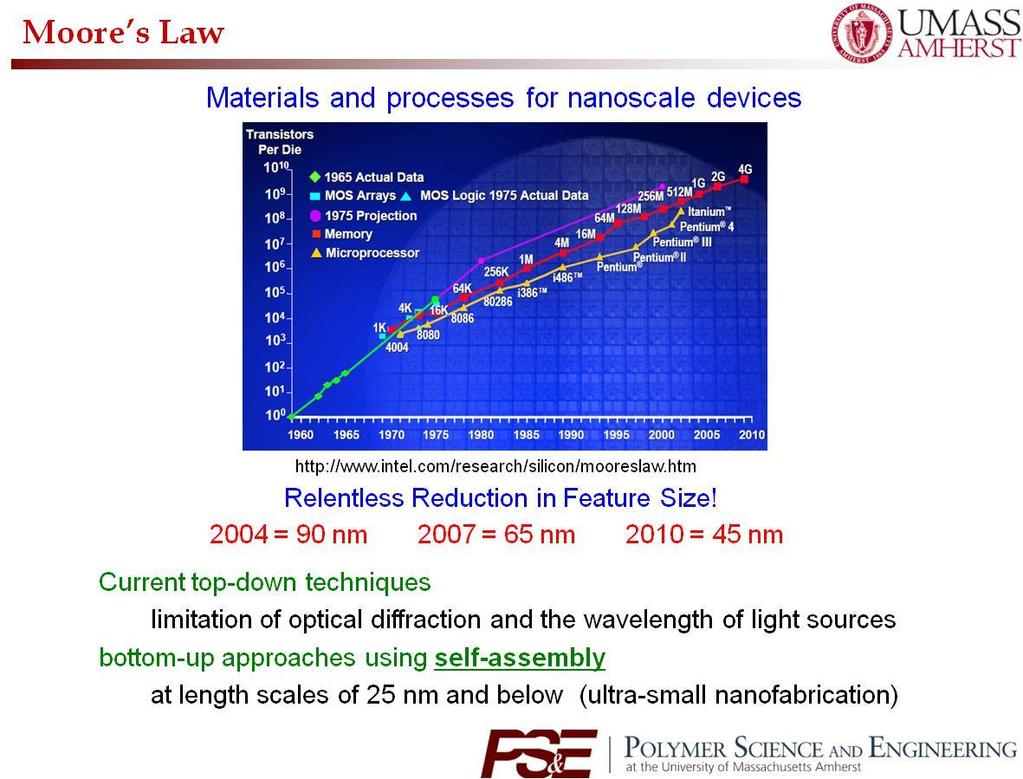
Macroscopic Arrays of Block Copolymers with Areal Densities of 10 Terbit/inch 2 and Beyond
|
|
|
- Cory Martin
- 6 years ago
- Views:
Transcription

1 Macroscopic Arrays of Block Copolymers with Areal Densities of 10 Terbit/inch 2 and Beyond Soojin Park*, Dong Hyun Lee, Bokyung Kim, Sung Woo Hong Department of Polymer Science and Engineering, University of Massachusetts, Amherst, MA *Ulsan National Institue of Science and Technology Shuaigang Xiao Seagate Technologies Ting Xu Department of Materials Science and Engineering & Department of Chemistry, University of California at Berkeley, Berkeley, CA Supported by: DOE BES, NSF MRSEC & CHM, Seagate Technologies
2
3
4
5

6 Russell, T.P., Physica B, 1995, 213&214, 22.
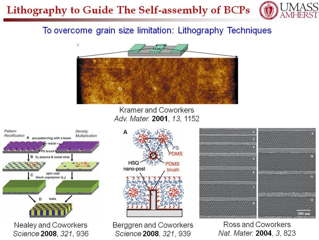
7 Balanced Interfacial Interactions Thermal Annealing UV Exposed


8 Application of Self-Assembled Block Copolymers Nanocrystal Flash Memory Semiconductor Capacitor Formation Applied Physics Letters (2001) Magnetic Data Storage Adv. Mater (2001) IEEE International Electron Devices 16 (2007) Nanoporous Membranes Magnetic Patterned Media Appl. Phys. Lett (2005) Low K Adv. Mater (2006) IEEE Trans Magn (2002)
 As-spun")

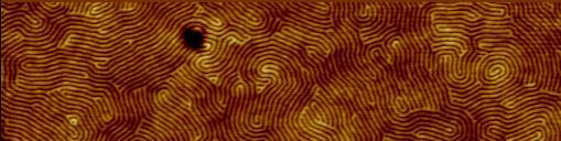
9 PS-b-PEO (19.0k-6.3k) As-spun film (~120 nm) Solvent annealed film
10 Grazing Incidence X-ray Scattering I ( q) ( ) E( ) E( ) Fs ( q) Ss( q) Fc ( q ) 2

11 GISAXS Patterns of PS-b-P4VP Thin Films As-spun 30 mins 1 hr hrs 3 hrs 4 hrs

12 Schematic diagram of solvent evaporation Solvent Evaporation f s Ordering Front r substrate DISORDERED ORDERED


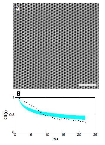
13 Schematic Diagram of Template Preparation Polystyrene-b-poly(4-vinylpyridine) (PS-b-P4VP) Spin coating Solvent annealing in Tol/THF Solvent mixture For 3-6 hrs in solvent vapor SFM Images As-spun 29.6 ± 5.9 nm Solvent annealing 25.0 ± 1.7 nm Scale bars: 200nm S. Park et al. ACS Nano 2008, 2, 766


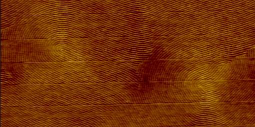
14 Reversible Reconstruction SFM image Solvent annealed film Reconstructed Film Recovery of initial morphology Solvent annealing in Toluene/THF Immersion in EtOH for 20 min Thermal annealing at 115 o C for 10 min Scale Bars: 200 nm (PS-b-P4VP: 47.6k-20.9k)
15


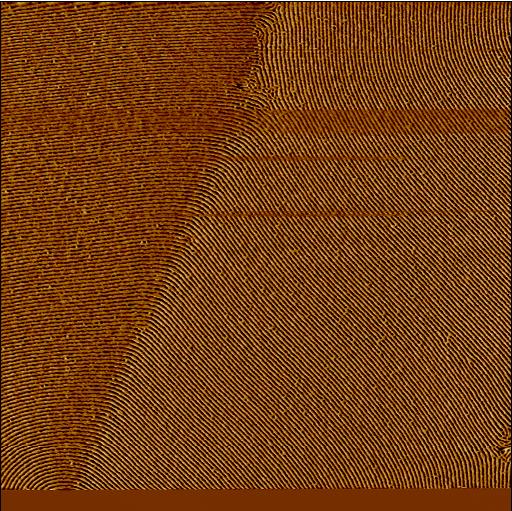
16 Macroscopic Arrays of BCP Microdomains Mis-cut Single Crystal Thermal Annealing Sawtooth Pattern Guided BCP Array Highly Ordered BCP Films Solvent Annealing Spin-coated BCP Film Spin-Coated BCP Film

 Phase mode PS-b-PEO")
 Phase mode")

 (2 µm x 2")
17 Highly Ordered PS-b-PEO Microdomains PS-b-PEO (20k-6.5k) Phase mode PS-b-PEO (19k-6.4k) Phase mode d-spacing: 30.2 nm Feature size: ~13 nm 0.74 Terabit/inch 2 (2 µm x 2 µm) (2 µm x 2 µm) d-spcing: 24.4 nm Feature size: 9.5 nm 1.21 Terabit/inch 2
 (Au complex) (1.5 µm x 1.")

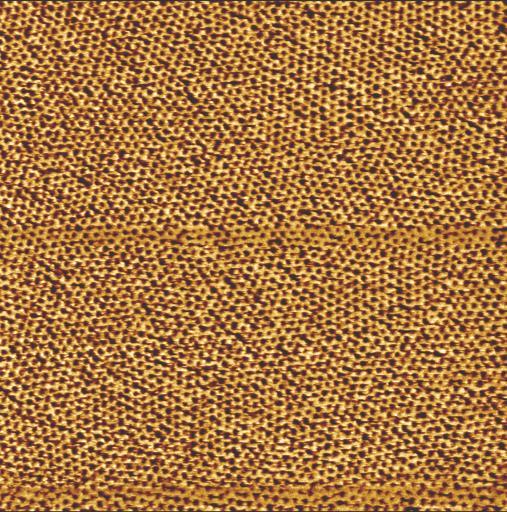
18 Highly Ordered PS-b-PEO Microdomains PS-b-PEO (16k-5k) PS-b-PEO (5k-2k) (Au complex) (1.5 µm x 1.5 µm) (1 µm x 1 µm) d-spacing: ~18.1 nm Feature size: ~ 7.8 nm 2.42 Terabit/inch 2 d-spacing: 6.93 nm Feature size: ~ 3.1 nm 10.5 terabit/inch 2
19 Orientational Ordering
20 Translational Ordering
21 Two-Dimensional Hexagonal Lattice (11) plane (10) plane Solid and dotted lines represent the symmetry planes perpendicular to the planes of paper Hexagonal lattice: (10), (11), (20), (21), (30), (22), (31), etc. Diffraction peaks: 1, 3, 4, 7, 9, 12, etc.

 0.0-1.0-0.5 0.0 0.5 1.0 2 f (deg.)")
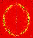
22 Log (I) (a.u.) GISAXS Patterns of Highly Ordered BCPs Log (I) (a.u.) Sample stage: 0 o Sample stage: 30 o f (deg.) q xy (nm -1 ) f (deg.) q xy (nm -1 ) f (deg.) f (deg.)
23 Nanoporous Materials from PS-b-PLA HO Cl + CuBr, PMDETA 110 o C, 12 h HO Cl n O O O O Sn(Oct) 2, Toluene 110 o C, 3 h HO m O O O O Cl n Biologically and Chemically Degradable Polymer
 2, Toluene 110 o C, 3 h")

24 Cl 110 o C, 12 h Nanoporous Materials from PS-b-PLA O O O O Sn(Oct) 2, Toluene 110 o C, 3 h HO m O O O O Cl n 0.5 Hexagonal Packing on Flat Substrate 0.0 f + i (deg.) -0.5 q q q 3q 500 nm 2q 2q -1.5
25
 q y (nm -1 ) 2 f (deg.) q y (nm -1 ) q z (nm -1 ) f (deg.) 1.8 1.6 1.5 1.4 1.2 1.0 0.8 0.6 0.5 0.4 0.2 0.")
26 q z (nm -1 ) f (deg.) o q z (nm -1 ) f (deg.) o Hx Packing of PS-b-PLA on Faceted Substrate d +0o > d +30o f (deg.) q y (nm -1 ) 2 f (deg.) q y (nm -1 ) q z (nm -1 ) f (deg.) o q z (nm -1 ) f (deg.) o f (deg.) q y (nm -1 ) 2 f (deg.) q y (nm -1 )

27 BCP Ordering Relative to Substrate

28 Pattern Transfer Process

29 Topography Transfer PDMS FEP 200 nm PI PBT

30 BCP Ordering on Soft, Flexible Substrate Reconstructed Sapphire PBT Replica PS-b-PEO Annealed in o-xylene vapor 2 mm x 2 mm

31 Transmission SAXS PS-b-PEO on PBT Replica 1 hr 2 hr 3 hr
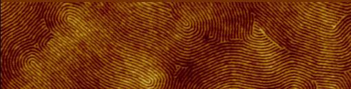
32 Imperfections: Parallel Alignment PS 20K -b-peo 6.5K Thin film 5 µm 5 µm


33 Parallel Alignment Perpendicular to Sawtooth Preliminary Results from Simulation J.Hu Yonsei, W.H.Jo, SNU 90 o no elastic penalty for gliding!!! (after removing major block)


34 Annihilation of Defects Thickness = 37 nm Thickness = 42 nm Height Height Trace of Annihilation 1 µm 1 µm 1 µm 1 µm The defects are effectively annihilated upon increasing the thickness!


35 Line Pattern with High Degree of Straightness Height Phase 2 µm 2 µm 2 µm 2 µm The defects are completely annihilated at the optimum thickness and annealing condition!

36 PERFECT or NOT? 0 o Only 3 sec, counts!!! 2 o 12 sec, counts 4 o 50 sec, There must be some defects by nature. However, the probability is less than 2%. The line pattern is highly aligned and oriented along one direction!
37 Solvent Annealing: on Hard Faceted Substrate Orientation Parameter (f) Normalized Intensity, I( ) Intensity at (1,0) Plane Rotation Angle, (rad.) cos 2 f I I 3 c s 2 cos sin d I sin d 2 cos sin d I 2 o 1 2 sin d f Orientation 1 Perfectly parallel 0 Random -0.5 Perfectly perpendicular


38 Transmission-SAXS Study: Pattern Transfer PBT Film Line Patterns on Polymeric Replica Pattern Transferring Solvent Annealing Polymeric Replica As-spun Film on Polymeric Replica

39 Transmission-SAXS Study: Pattern Transfer Peak Positions are same! The line pattern is highly aligned and oriented along one direction!
Vertically aligned Ni magnetic nanowires fabricated by diblock-copolymer-directed Al thin film anodization
 Vertically aligned Ni magnetic nanowires fabricated by diblock-copolymer-directed Al thin film anodization Researcher: Kunbae (Kevin) Noh, Graduate Student, MAE Dept. and CMRR Collaborators: Leon Chen,
Supporting information. In-situ TEM observation of phase transition of nanoscopic patterns on. baroplastic block copolymer film during nanoindentation
 Supporting information In-situ TEM observation of phase transition of nanoscopic patterns on baroplastic block copolymer film during nanoindentation Ara Jo, Gil Ho Gu, Hong Chul Moon, Sung Hyun Han, Sang
Three-dimensionally Packed Nano-helical Phase. in Chiral Block Copolymers
 Three-dimensionally Packed Nano-helical Phase in Chiral Block Copolymers Rong-Ming Ho, Yeo-Wan Chiang, Chi-Chun Tsai, Chu-Chieh Lin, Bao-Tsan Ko, Bor-Han Huang Supporting Information Table S1 Table S2
BLOCK COPOLYMER PHOTONIC GEL FOR DETECTING INTERFACIAL SEPARATION
 BLOCK COPOLYMER PHOTONIC GEL FOR DETECTING INTERFACIAL SEPARATION Edwin P. Chan, Materials Research Engineer, National Institute of Standards and Technology, Gaithersburg, MD Introduction Mechanochromism,
Holey Silicon as efficient thermoelectric material
 Supporting Information: Holey Silicon as efficient thermoelectric material Jinyao Tang 1, 3*, Hung-Ta Wang 1*, Dong Hyun Lee 4, Melissa Fardy 1, Ziyang Huo 1, Thomas P. Russell 4, 1, 2, 3 Peidong Yang
RESEARCH BACKGROUND (Postdoc+) (MS + INDUSTRY) (PHD)
 (MS + INDUSTRY) (PHD)") RESEARCH BACKGROUND 1998-2006 (MS + INDUSTRY) Pilot, lab and full scale studies of membranes and other water treatment technologies Desalination major focus 2006-2010 (PHD) Biomimetic membranes! Earliest
RESEARCH BACKGROUND 1998-2006 (MS + INDUSTRY) Pilot, lab and full scale studies of membranes and other water treatment technologies Desalination major focus 2006-2010 (PHD) Biomimetic membranes! Earliest
Towards scalable fabrication of high efficiency polymer solar cells
 Towards scalable fabrication of high efficiency polymer solar cells Hui Joon Park 2*, Myung-Gyu Kang 1**, Se Hyun Ahn 3, Moon Kyu Kang 1, and L. Jay Guo 1,2,3 1 Department of Electrical Engineering and
Monte Carlo approach to island formation during thermal treatment of thin films*
 Monte Carlo approach to island formation during thermal treatment of thin films* Ann Marie Hardin December 6, 2006 *F. Lallet, R. Bachelet, A. Dauger, and N. Olivi-Tran, (2006) Physical Review B, 74 Outline
Anisotropic Mechanical Properties of Pr(Co,In) 5 -type Compounds and Their Relation to Texture Formation in Die-upset Magnets
 5 -type Compounds and Their Relation to Texture Formation in Die-upset Magnets") Journal of Magnetics 16(3), 220-224 (2011) http://dx.doi.org/10.4283/jmag.2011.16.3.220 Anisotropic Mechanical Properties of Pr(Co,In) 5 -type Compounds and Their Relation to Texture Formation in Die-upset
Journal of Magnetics 16(3), 220-224 (2011) http://dx.doi.org/10.4283/jmag.2011.16.3.220 Anisotropic Mechanical Properties of Pr(Co,In) 5 -type Compounds and Their Relation to Texture Formation in Die-upset
Preparation and structural characterization of thin-film CdTe/CdS heterojunctions
 JOURNAL OF OPTOELECTRONICS AND ADVANCED MATERIALS Vol. 8, No., June 006, p. 96-940 Preparation and structural characterization of thin-film CdTe/ heterojunctions I. SALAORU a, P. A. BUFFAT b, D. LAUB b,
Soft-lithography for Preparing Patterned Liquid Crystal Orientations
 2007 KIDS Soft-lithography for Preparing Patterned Liquid Crystal Orientations Hak-Rin Kim **a, Jong-Wook Jung **a, Min-Soo Shin **a, Myung-Eun Kim a, You-Jin Lee **a, and Jae-Hoon Kim *b Abstract We demonstrate
Shear Bands in Glassy Amorphous Polymers
 Shear Bands in Glassy Amorphous Polymers Shear banding in tension or compression. Neck formation via shear bands (a) (b) (c) (d) Stress Image removed due to copyright restrictions. Please see Fig. 12a
Multiphoton lithography based 3D micro/nano printing Dr Qin Hu
 Multiphoton lithography based 3D micro/nano printing Dr Qin Hu EPSRC Centre for Innovative Manufacturing in Additive Manufacturing University of Nottingham Multiphoton lithography Also known as direct
Structures of AlN/VN superlattices with different AlN layer thicknesses
 Structures of AlN/VN superlattices with different AlN layer thicknesses Quan Li a) Department of Physics, The Chinese University of Hong Kong, Shatin, New Territory, Hong Kong I.W. Kim, S.A. Barnett, and
Nonlinear Thickness and Grain Size Effects on the Thermal Conductivity of CuFeSe 2 Thin Films
 CHINESE JOURNAL OF PHYSICS VOL. 51, NO. 1 February 2013 Nonlinear Thickness and Grain Size Effects on the Thermal Conductivity of CuFeSe 2 Thin Films P. C. Lee, 1, 2, 3, M. N. Ou, 3 Z. W. Zhong, 3 J. Y.
Thin Film Scattering: Epitaxial Layers
 Thin Film Scattering: Epitaxial Layers 6th Annual SSRL Workshop on Synchrotron X-ray Scattering Techniques in Materials and Environmental Sciences: Theory and Application May 29-31, 2012 Thin films. Epitaxial
Supplementary Figure 1 Dependence of the capacitace of PVP:HDA dielectric layer with
 Capacitance (F/m 2 ) 1.4x10⁻⁴ 1.2x10⁻⁴ 1.0x10⁻⁴ 8.0x10⁻⁵ 6.0x10⁻⁵ 4.0x10⁻⁵ 2.0x10⁻⁵ 100 1k 10k 100k 1M Frequency (Hz) Supplementary Figure 1 Dependence of the capacitace of PVP:HDA dielectric layer with
Catherine G. Reyes, Anshul Sharma and Jan P.F. Lagerwall. July 18, Complete description of experimental details
 Non-electronic gas sensor from electrospun mats of liquid crystal core fibers for detecting volatile organic compounds at room temperature: Supplemental Online Material Catherine G. Reyes, Anshul Sharma
White Paper: Pixelligent Internal Light Extraction Layer for OLED Lighting
 White Paper: Pixelligent Internal Light Zhiyun (Gene) Chen, Ph.D., Vice President of Engineering Jian Wang, Ph.D., Manager, Application Engineering Pixelligent Technologies LLC, 6411 Beckley Street, Baltimore,
Growth of YBa 2 Cu 3 O 7 Films with [110] Tilt of CuO Planes to Surface on SrTiO 3 Crystals
![Growth of YBa 2 Cu 3 O 7 Films with [110] Tilt of CuO Planes to Surface on SrTiO 3 Crystals](/thumbs/72/67895252.jpg "Growth of YBa 2 Cu 3 O 7 Films with [110] Tilt of CuO Planes to Surface on SrTiO 3 Crystals") ISSN 163-7745, Crystallography Reports, 213, Vol. 58, No. 3, pp. 488 492. Pleiades Publishing, Inc., 213. Original Russian Text E.A. Stepantsov, F. Lombardi, D. Winkler, 213, published in Kristallografiya,
ISSN 163-7745, Crystallography Reports, 213, Vol. 58, No. 3, pp. 488 492. Pleiades Publishing, Inc., 213. Original Russian Text E.A. Stepantsov, F. Lombardi, D. Winkler, 213, published in Kristallografiya,
Nanoimprinting in Polymers and Applications in Cell Studies. Albert F. YEE Chemical Engineering & Materials Science UC Irvine
 Nanoimprinting in Polymers and Applications in Cell Studies Albert F. YEE Chemical Engineering & Materials Science UC Irvine Presentation outline Motivation Reversal imprinting Soft inkpad imprinting on
Probing the Self-Organization Kinetics in Block Copolymer Films
 Mater. Res. Soc. Symp. Proc. Vol. 1147 2009 Materials Research Society 1147-OO01-01 Probing the Self-Organization Kinetics in Block Copolymer Films Detlef-M. Smilgies 1, Ruipeng Li 1,2, Zhenyu Di 3, Charles
Aligned Carbon Nanofibre-Polymer Composite Membranes. CNT Growth and Manipulation. Eleanor Campbell Dept. of Physics, Göteborg University
 Aligned Carbon Nanofibre-Polymer Composite Membranes CNT Growth and Manipulation Eleanor Campbell Dept. of Physics, Göteborg University Plasma CVD Growth Polymer/Nanofibre Composite Low ambient temperature
Universität Hamburg, Hamburg, Germany. Universität Hamburg, Hamburg, Germany
 Sample Preparation, Micromagnetic Simulations, Circular-Rotational Currents, Parasitic Oersted Fields and Clover Samples (Magnetic Antivortex-Core Reversal by Circular-Rotational Spin Currents) Thomas
6.8 Magnetic in-plane anisotropy of epitaxially grown Fe-films on vicinal Ag(001) and Au(001) with different miscut orientations
 and Au(001) with different miscut orientations") C. Epitaxial Growth 6.8 Magnetic in-plane anisotropy of epitaxially grown Fe-films on vicinal Ag(001) and Au(001) with different miscut orientations M. Rickart, A.R. Frank, J. Jorzick, Ch. Krämer, S.O.
C. Epitaxial Growth 6.8 Magnetic in-plane anisotropy of epitaxially grown Fe-films on vicinal Ag(001) and Au(001) with different miscut orientations M. Rickart, A.R. Frank, J. Jorzick, Ch. Krämer, S.O.
Light enhancement by the formation of an Al-oxide honeycomb nano-structure on the n-gan surface of thin-gan light-emitting diodes
 Light enhancement by the formation of an Al-oxide honeycomb nano-structure on the n-gan surface of thin-gan light-emitting diodes C. L. Lin, P. H. Chen Department of Chemical and Materials Engineering,
What if your diffractometer aligned itself?
 Ultima IV Perhaps the greatest challenge facing X-ray diffractometer users today is how to minimize time and effort spent on reconfiguring of the system for different applications. Wade Adams, Ph.D., Director,
Fabrication of aligned metallic structures based on block copolymer lithography
 88 Fabrication of aligned metallic structures based on block copolymer lithography Yusuke Takahashi Department ofmicroelectronic Engineering, Rochester Institute of Technology, 82 Lomb Memorial Dr., Rochester,
Supporting Information. Flexible, Low-Power Thin-Film Transistors (TFTs) Made of Vapor-Phase. Synthesized High-k, Ultrathin Polymer Gate Dielectrics
 Made of Vapor-Phase. Synthesized High-k, Ultrathin Polymer Gate Dielectrics") Supporting Information Flexible, Low-Power Thin-Film Transistors (TFTs) Made of Vapor-Phase Synthesized High-k, Ultrathin Polymer Gate Dielectrics Junhwan Choi, Munkyu Joo, Hyejeong Seong, Kwanyong Pak,
Supporting Information Flexible, Low-Power Thin-Film Transistors (TFTs) Made of Vapor-Phase Synthesized High-k, Ultrathin Polymer Gate Dielectrics Junhwan Choi, Munkyu Joo, Hyejeong Seong, Kwanyong Pak,
Nanostructured Engineered Materials With High Magneto-optic Performance For Integrated Photonics Applications
 Edith Cowan University Research Online School of Engineering Publications 28 Nanostructured Engineered Materials With High Magneto-optic Performance For Integrated Photonics Applications Mikhail Vasiliev
Damage Threats and Response of Final Optics for Laser-Fusion Power Plants
 Damage Threats and Response of Final Optics for Laser-Fusion Power Plants M. S. Tillack 1, S. A. Payne 2, N. M. Ghoniem 3, M. R. Zaghloul 1 and J. F. Latkowski 2 1 UC San Diego, La Jolla, CA 92093-0417
High-Resolution, Electrohydrodynamic Inkjet Printing of Stretchable, Metal Oxide Semiconductor Transistors with High Performances
 Electronic Supplementary Material (ESI) for Nanoscale. This journal is The Royal Society of Chemistry 2016 ` Electronic Supplementary Information High-Resolution, Electrohydrodynamic Inkjet Printing of
High Resolution X-ray Diffraction
 High Resolution X-ray Diffraction Nina Heinig with data from Dr. Zhihao Donovan Chen, Panalytical and slides from Colorado State University Outline Watlab s new tool: Panalytical MRD system Techniques:
This journal is The Royal Society of Chemistry S 1
 2013 S 1 Thermochemical analysis on the growth of NiAl 2 O 4 rods Sang Sub Kim, a Yong Jung Kwon, b Gunju Sun, a Hyoun Woo Kim,* b and Ping Wu* c a Department of Materials Science and Engineering, Inha
Earth & Planetary Science Applications of X-Ray Diffraction: Advances Available for Research with our New Systems
 Earth & Planetary Science Applications of X-Ray Diffraction: Advances Available for Research with our New Systems James R. Connolly Dept. of Earth & Planetary Sciences University of New Mexico 401/501
Lecture 5. SOI Micromachining. SOI MUMPs. SOI Micromachining. Silicon-on-Insulator Microstructures. Agenda:
 EEL6935 Advanced MEMS (Spring 2005) Instructor: Dr. Huikai Xie SOI Micromachining Agenda: SOI Micromachining SOI MUMPs Multi-level structures Lecture 5 Silicon-on-Insulator Microstructures Single-crystal
NanoSystemsEngineering: NanoNose Final Status, March 2011
 1 NanoSystemsEngineering: NanoNose Final Status, March 2011 The Nanonose project is based on four research projects (VCSELs, 3D nanolithography, coatings and system integration). Below, the major achievements
TEM imaging and diffraction examples
 TEM imaging and diffraction examples Duncan Alexander EPFL-CIME 1 Diffraction examples Kikuchi diffraction Epitaxial relationships Polycrystalline samples Amorphous materials Contents Convergent beam electron
Experiment 2b X-Ray Diffraction* Optical Diffraction Experiments
 * Experiment 2b X-Ray Diffraction* Adapted from Teaching General Chemistry: A Materials Science Companion by A. B. Ellis et al.: ACS, Washington, DC (1993). Introduction Inorganic chemists, physicists,
Supplementary information. Guided fracture of films on soft substrates to create micro/nano-feature. arrays with controlled periodicity
 Supplementary information Guided fracture of films on soft substrates to create micro/nano-feature arrays with controlled periodicity Byoung Choul Kim 1,2, Toshiki Matsuoka 1, Christopher Moraes 1, Jiexi
Supporting Information
 Supporting Information Controlled Vapor Phase Growth of Single Crystalline, Two-Dimensional GaSe Crystals with High Photoresponse Xufan Li, Ming-Wei Lin, Alexander A. Puretzky, Juan C. Idrobo, Cheng Ma,
X-Ray Diffraction by Macromolecules
 N. Kasai M. Kakudo X-Ray Diffraction by Macromolecules With 351 Figures and 56 Tables Kodansha ~Springer ... Contents Preface v Part I Fundamental 1. Essential Properties of X-Rays................. 3 1.1
Growth and Doping of SiC-Thin Films on Low-Stress, Amorphous Si 3 N 4 /Si Substrates for Robust Microelectromechanical Systems Applications
 Journal of ELECTRONIC MATERIALS, Vol. 31, No. 5, 2002 Special Issue Paper Growth and Doping of SiC-Thin Films on Low-Stress, Amorphous Si 3 N 4 /Si Substrates for Robust Microelectromechanical Systems
Instrument Configuration for Powder Diffraction
 Instrument Configuration for Powder Diffraction Advanced X-ray Workshop S.N. Bose National Centre for Basic Sciences, 14-15/12/2011 Innovation with Integrity Overview What is the application? What are
Soft Lithography. Jin-Goo Park. Materials and Chemical Engineering Hanyang University, Ansan. Electronic Materials and Processing Lab.
 Hanyang University Soft Lithography Jin-Goo Park Materials and Chemical Engineering Hanyang University, Ansan Electronic Materials and Processing Lab. Introduction to Soft Lithography Research Micro- Electro-
Chapter Outline How do atoms arrange themselves to form solids?
 Chapter Outline How do atoms arrange themselves to form solids? Fundamental concepts and language Unit cells Crystal structures Face-centered cubic Body-centered cubic Hexagonal close-packed Close packed
Thermal Stability of Liquid Crystal Alignment Layers Prepared by In-Situ Ultra-Violet Exposure during Imidization of Polyimide
 Jpn. J. Appl. Phys. Vol. 40 (001) pp. 381 386 Part 1, No. 4A, April 001 c 001 The Japan Society of Applied Physics Thermal Stability of Liquid Crystal Alignment Layers Prepared by In-Situ Ultra-Violet
Applications of Successive Ionic Layer Adsorption and Reaction (SILAR) Technique for CZTS Thin Film Solar Cells
 Technique for CZTS Thin Film Solar Cells") NANO VISION An International Open Free Access, Peer Reviewed Research Journal www.nano-journal.org ISSN 2231-2579 (Print) ISSN 2319-7633 (Online) Abbr: Nano Vision. 2013, Vol.3(3): Pg.235-239 Applications
NANO VISION An International Open Free Access, Peer Reviewed Research Journal www.nano-journal.org ISSN 2231-2579 (Print) ISSN 2319-7633 (Online) Abbr: Nano Vision. 2013, Vol.3(3): Pg.235-239 Applications
Relation Between Internal Stress and Surface Roughness of Titanium Nitride Films Deposited by HCD Ion Plating
 No.22,28 65 Relation Between Internal Stress and Surface Roughness of Titanium Nitride Films Deposited by HCD Ion Plating Itsuo Ishigami Ken-ichi Miura Hideaki Hoshino Tomoyuki Mizukoshi (28 6 17 ) An
Annealing Effect on Elastic Constant of Ultrathin Films Studied by Acoustic-Phonon Resonance Spectroscopy
 1st International Symposium on Laser Ultrasonics: Science, Technology and Applications July 16-18 28, Montreal, Canada Annealing Effect on Elastic Constant of Ultrathin Films Studied by Acoustic-Phonon
Twins & Dislocations in HCP Textbook & Paper Reviews. Cindy Smith
 Twins & Dislocations in HCP Textbook & Paper Reviews Cindy Smith Motivation Review: Outline Crystal lattices (fcc, bcc, hcp) Fcc vs. hcp stacking sequences Cubic {hkl} naming Hcp {hkil} naming Twinning
Lectures on: Introduction to and fundamentals of discrete dislocations and dislocation dynamics. Theoretical concepts and computational methods
 Lectures on: Introduction to and fundamentals of discrete dislocations and dislocation dynamics. Theoretical concepts and computational methods Hussein M. Zbib School of Mechanical and Materials Engineering
Surface Preparation and Cleaning Conference April 19-20, 2016, Santa Clara, CA, USA. Nano-Bio Electronic Materials and Processing Lab.
 Surface Preparation and Cleaning Conference April 19-20, 2016, Santa Clara, CA, USA Issues on contaminants on EUV mask Particle removal on EUV mask surface Carbon contamination removal on EUV mask surface
1 Thin-film applications to microelectronic technology
 1 Thin-film applications to microelectronic technology 1.1 Introduction Layered thin-film structures are used in microelectronic, opto-electronic, flat panel display, and electronic packaging technologies.
Topological crystalline insulators. Tomasz Story Institute of Physics, Polish Academy of Sciences, Warsaw
 Topological crystalline insulators Tomasz Story Institute of Physics, Polish Academy of Sciences, Warsaw Topological crystalline insulators - outline 1. Introduction topological crystalline insulators
Free standing Multilayer Thin Film of Cellulose Nanocrystals
 Free standing Multilayer Thin Film of Cellulose Nanocrystals Chaoyang Jiang Department of Chemistry The University of South Dakota Edmonton, June 25, 2009 Cellulose Nanocrystals Nanotechnology R&D Priority
Correlating the scattered intensities of P3HT and PCBM to the current. densities of polymer solar cells
 Supplementary Information for Correlating the scattered intensities of P3HT and PCBM to the current densities of polymer solar cells Enrique D. Gomez*, Katherine P. Barteau, He Wang, Michael F. Toney,
INVESTIGATION OF NANOCRYSTALS USING TEM MICROGRAPHS AND ELECTRON DIFFRACTION TECHNIQUE
 INVESTIGATION OF NANOCRYSTALS USING TEM MICROGRAPHS AND ELECTRON DIFFRACTION TECHNIQUE CAMELIA OPREA, VICTOR CIUPINA, GABRIEL PRODAN Department of Physics, Ovidius University, Constanþa, 900527, Romania
High-efficiency GaN-based light-emitting diodes fabricated with identical Ag contact formed on both n- and p-layers
 High-efficiency GaN-based light-emitting diodes fabricated with identical Ag contact formed on both n- and p-layers Munsik Oh and Hyunsoo Kim * School of Semiconductor and Chemical Engineering and Semiconductor
Supporting Information
 Supporting Information Fast-Response, Sensitivitive and Low-Powered Chemosensors by Fusing Nanostructured Porous Thin Film and IDEs-Microheater Chip Zhengfei Dai,, Lei Xu,#,, Guotao Duan *,, Tie Li *,,
Chapter Outline. How do atoms arrange themselves to form solids?
 Chapter Outline How do atoms arrange themselves to form solids? Fundamental concepts and language Unit cells Crystal structures! Face-centered cubic! Body-centered cubic! Hexagonal close-packed Close packed
Fabrication of Ru/Bi 4-x La x Ti 3 O 12 /Ru Ferroelectric Capacitor Structure Using a Ru Film Deposited by Metalorganic Chemical Vapor Deposition
 Mat. Res. Soc. Symp. Proc. Vol. 784 2004 Materials Research Society C7.7.1 Fabrication of Ru/Bi 4-x La x Ti 3 O 12 /Ru Ferroelectric Capacitor Structure Using a Ru Film Deposited by Metalorganic Chemical
Performance at Wafer-Scale
 Supporting Information Self-Assembling VO 2 Nanonet with High Switching Performance at Wafer-Scale Jiasong Zhang, Haibo Jin*, Zhuo Chen, Maosheng Cao, Pengwan Chen, Yankun Dou, Yongjie Zhao, Jingbo Li*
Surface plasmon enhanced emission from dye doped polymer layers
 Surface plasmon enhanced emission from dye doped polymer layers Terrell D. Neal, a) Koichi Okamoto, and Axel Scherer Department of Electrical Engineering, California Institute of Technology, Pasadena,
Growth Of TiO 2 Films By RF Magnetron Sputtering Studies On The Structural And Optical Properties
 Journal of Multidisciplinary Engineering Science and Technology (JMEST) Growth Of TiO 2 Films By RF Magnetron Sputtering Studies On The Structural And Optical Properties Ahmed K. Abbas 1, Mohammed K. Khalaf
350 C for 8 hours in argon atmosphere. Supplementary Figures. Supplementary Figure 1 High-temperature annealing of BP flakes on SiO 2.
 Supplementary Figures Supplementary Figure 1 High-temperature annealing of BP flakes on SiO 2. (a-d) The optical images of three BP flakes on a SiO 2 substrate before (a,b) and after annealing (c,d) at
3. Anisotropic blurring by dislocations
 Dynamical Simulation of EBSD Patterns of Imperfect Crystals 1 G. Nolze 1, A. Winkelmann 2 1 Federal Institute for Materials Research and Testing (BAM), Berlin, Germany 2 Max-Planck- Institute of Microstructure
Hydrothermal Synthesis of Nano-sized PbTiO3 Powder and Epitaxial Film for Memory Capacitor Application
 American Journal of Materials Science and Technology (2012) 1: 22-27 doi:10.7726/ajmst.2012.1004 Research Article Hydrothermal Synthesis of Nano-sized PbTiO3 Powder and Epitaxial Film for Memory Capacitor
Barix Multilayers: a Water and Oxygen Barrier for Flexible Organic Electronics. Robert Jan Visser
 Barix Multilayers: a Water and Oxygen Barrier for Flexible Organic Electronics Robert Jan Visser Organic Electronics Is the Future of Electronics Organic? MIT Stanford UC Berkeley Nano Forum Vitex Systems,
Single Crystalline Co 3 O 4 Nanocrystals Exposed with Different Crystal Planes for Li-O 2 Batteries
 Supplementary Information Single Crystalline Co 3 O 4 Nanocrystals Exposed with Different Crystal Planes for Li-O 2 Batteries Dawei Su, 1,2* Shixue Dou, 1* and Guoxiu Wang 2* 1 Institute for Superconducting
3.7GHz, Low Loss, 100MHz Bandwidth, Single Crystal, Aluminum Nitride on Silicon Carbide Substrate (AlN-on-SiC) BAW Filter
 BAW Filter") 3.7GHz, Low Loss, 100MHz Bandwidth, Single Crystal, Aluminum Nitride on Silicon Carbide Substrate (AlN-on-SiC) BAW Filter Presented by Rama Vetury Akoustis Technologies, Inc. Outline of this Presentation
3.7GHz, Low Loss, 100MHz Bandwidth, Single Crystal, Aluminum Nitride on Silicon Carbide Substrate (AlN-on-SiC) BAW Filter Presented by Rama Vetury Akoustis Technologies, Inc. Outline of this Presentation
OUTLINE. Preparation of III Nitride thin 6/10/2010
 Preparation of III Nitride thin films for LEDs Huaxiang Shen Supervisor: Dr. Adrian Kitai 1 2 Two kinds of EL devices Light emitting diodes Powder EL and thin film EL http://en.wikipedia.org/wiki/file:pnjunction
ICFM313 Characterization Study of Copper Thin Film Coated on Steel Substrateby Thermal Evaporation Technique. Abstract
 ICFM313 Characterization Study of Copper Thin Film Coated on Steel Substrateby Thermal Evaporation Technique SuganthiJ a Johnsonjeyakumar b SudhaJ a a Department of Physics, Sri ChandrasekharendraSaraswathiViswaMahavidyalaya
It is instructive however for you to do a simple structure by hand. Rocksalt Structure. Quite common in nature. KCl, NaCl, MgO
 Today the structure determinations etc are all computer -assisted It is instructive however for you to do a simple structure by hand Rocksalt Structure Quite common in nature KCl, NaCl, MgO 9-1 Typical
Effect of grain size on the mobility and transfer characteristics of polysilicon thin-film transistors
 Indian Journal of Pure & Applied Physics Vol. 42, July 2004, pp 528-532 Effect of grain size on the mobility and transfer characteristics of polysilicon thin-film transistors Navneet Gupta* & B P Tyagi**
2-inch polycrystalline silicon thin film transistor array. using field aided lateral crystallization
 2-inch polycrystalline silicon thin film transistor array using field aided lateral crystallization JAE HOON JUNG, MYEONG HO KIM, YOUNG BAE KIM a, DUCK-KYUN CHOI, Division of Materials Science and Engineering,
What is a positron moderator?
 What is a positron moderator? The advent of slow positron beams has resulted in nondestructive depth profiling of defects in surfaces and interfaces, low energy positron diffraction and positron remission
Imprint lithography for curved cross-sectional structure using replicated Ni mold
 Imprint lithography for curved cross-sectional structure using replicated Ni mold Yoshihiko Hirai, a) Satoshi Harada, Hisao Kikuta, and Yoshio Tanaka Mechanical System Engineering, Graduate School of Engineering,
Light Trapping Enhancement in Thin Film Silicon Solar Cell with Different Back Reflector
 International Journal of Electrical Components and Energy Conversion 2017; 3(5): 83-87 http://www.sciencepublishinggroup.com/j/ijecec doi: 10.11648/j.ijecec.20170305.11 ISSN: 2469-8040 (Print); ISSN: 2469-8059
 Defects in solids http://www.bath.ac.uk/podcast/powerpoint/inaugural_lecture_250407.pdf http://www.materials.ac.uk/elearning/matter/crystallography/indexingdirectionsandplanes/indexing-of-hexagonal-systems.html
Small-angle X-ray scattering (SAXS) with synchrotron radiation
 with synchrotron radiation") Small-angle X-ray scattering (SAXS) with synchrotron radiation Martin Müller Institut für Experimentelle und Angewandte Physik der Christian-Albrechts-Universität zu Kiel Introduction to small-angle scattering
Small-angle X-ray scattering (SAXS) with synchrotron radiation Martin Müller Institut für Experimentelle und Angewandte Physik der Christian-Albrechts-Universität zu Kiel Introduction to small-angle scattering
Exchange bias of polycrystalline antiferromagnets with perfectly compensated interfaces
 Exchange bias of polycrystalline antiferromagnets with perfectly compensated interfaces D. Suess,* M. Kirschner, T. Schrefl, and J. Fidler Institute of Solid State Physics, Vienna University of Technology,
Carbon Nanotube-Based Supercapacitors with Excellent AC-Line
 SUPPORTING INFORMATION FOR: Carbon Nanotube-Based Supercapacitors with Excellent AC-Line Filtering and Rate Capability via Improved Interfacial Impedance Yverick Rangom, Xiaowu (Shirley) Tang*, and Linda
Anomaly of Film Porosity Dependence on Deposition Rate
 Anomaly of Film Porosity Dependence on Deposition Rate Stephen P. Stagon and Hanchen Huang* Department of Mechanical Engineering, University of Connecticut, Storrs, CT 06269 J. Kevin Baldwin and Amit Misra
STRUCTURAL PROPERTIES AND COMPOSITION ANALYSIS OF Cu Ni Co ALLOY THIN FILM
 SOLID STATE PHYSICS STRUCTURAL PROPERTIES AND COMPOSITION ANALYSIS OF Cu Ni Co ALLOY THIN FILM V. CIUPINĂ 1, G. PRODAN 1, V. IONESCU 1, C. CASAPU 1, D. MANOLE 1, D. TUDORAN 1, E. VASILE 2, I. M. OANCEA
Lessons learned while watching paint dry: film formation, drying fronts, and cracking
 Lessons learned while watching paint dry: film formation, drying fronts, and cracking William B. Russel Department of Chemical Engineering Princeton University Procter and Gamble July 2007 OUTLINE one-dimensional
Journal of Chemical and Pharmaceutical Research, 2017, 9(1): Research Article
: Research Article") Available online www.jocpr.com Journal of Chemical and Pharmaceutical Research, 2017, 9(1):163-167 Research Article ISSN : 0975-7384 CODEN(USA) : JCPRC5 Synthesis and Characterization of Carbon Nano Spheres
Available online www.jocpr.com Journal of Chemical and Pharmaceutical Research, 2017, 9(1):163-167 Research Article ISSN : 0975-7384 CODEN(USA) : JCPRC5 Synthesis and Characterization of Carbon Nano Spheres
Recrystallization in CdTe/CdS
 Thin Solid Films 361±362 (2000) 420±425 www.elsevier.com/locate/tsf Recrystallization in CdTe/CdS A. Romeo, D.L. BaÈtzner, H. Zogg, A.N. Tiwari* Thin Film Physics Group, Institute of Quantum Electronics,
High Sensitivity of Phase-based Surface Plasmon Resonance in Nano-cylinder Array
 PIERS ONLINE, VOL. 4, NO. 7, 2008 746 High Sensitivity of Phase-based Surface Plasmon Resonance in Nano-cylinder Array Bing-Hung Chen, Yih-Chau Wang, and Jia-Hung Lin Institute of Electronic Engineering,
Introduction to Micro/Nano Fabrication Techniques. Date: 2015/05/22 Dr. Yi-Chung Tung. Fabrication of Nanomaterials
 Introduction to Micro/Nano Fabrication Techniques Date: 2015/05/22 Dr. Yi-Chung Tung Fabrication of Nanomaterials Top-Down Approach Begin with bulk materials that are reduced into nanoscale materials Ex:
Grain Sizes and Surface Roughness in Platinum and Gold Thin Films. L.L. Melo, A. R. Vaz, M.C. Salvadori, M. Cattani
 Journal of Metastable and Nanocrystalline Materials Vols. 20-21 (2004) pp. 623-628 online at http://www.scientific.net 2004 Trans Tech Publications, Switzerland Grain Sizes and Surface Roughness in Platinum
New Cu-based Bulk Metallic Glasses with High Strength of 2000 MPa
 Materials Science Forum Online: 2004-03-15 ISSN: 1662-9752, Vols. 449-452, pp 945-948 doi:10.4028/www.scientific.net/msf.449-452.945 2004 Trans Tech Publications, Switzerland New Cu-based Bulk Metallic
O2 Plasma Damage and Dielectric Recoveries to Patterned CDO Low-k Dielectrics
 O2 Plasma Damage and Dielectric Recoveries to Patterned CDO Low-k Dielectrics H. Huang 1, J. Bao 1, H. Shi 1, P. S. Ho 1, M L McSwiney 2, M D Goodner 2, M Moinpour 2, and G M Kloster 2 1 Laboratory for
Integration of Block-Copolymer with Nano- Imprint Lithography: Pushing the Boundaries of Emerging Nano-Patterning Technology
 Integration of Block-Copolymer with Nano- Imprint Lithography: Pushing the Boundaries of Emerging Nano-Patterning Technology April 2010 update SNL Geoff Brennecka (PI) Bruce Burckel Matt George Jack Skinner
Micro Injection Molding of Micro Fluidic Platform
 Micro Injection Molding of Micro Fluidic Platform S. C. Chen, J. A. Chang, Y. J. Chang and S. W. Chau Department of Mechanical Engineering, Chung Yuan University, Taiwan, ROC Abstract In this study, micro
Si-containing block copolymers for self-assembled nanolithography
 Si-containing block copolymers for self-assembled nanolithography C. A. Ross, a Y. S. Jung, V. P. Chuang, and F. Ilievski Department of Materials Science and Engineering, Massachusetts Institute of Technology,
New generation of solar cell technologies
 New generation of solar cell technologies Emerging technologies and their impact on the society 9th March 2017 Dhayalan Velauthapillai Professor, Faculty of Engineering and Business Administration Campus
Merging Bottom-Up with Top-Down: Continuous Lamellar Networks and Block Copolymer Lithography
 University of Colorado, Boulder CU Scholar Chemical & Biological Engineering Graduate Theses & Dissertations Chemical & Biological Engineering Spring 1-1-2014 Merging Bottom-Up with Top-Down: Continuous
Morphology of Cadmium Sulfide/Poly(ethylene)Oxide Nanocomposites
Oxide Nanocomposites") ISSN: 2319-7706 Volume 3 Number 9 (2014) pp. 469-473 http://www.ijcmas.com Original Research Article Morphology of Cadmium Sulfide/Poly(ethylene)Oxide Nanocomposites V.S.Sangawar and R.N.Bhagat* Polymer/Nanomaterials
ISSN: 2319-7706 Volume 3 Number 9 (2014) pp. 469-473 http://www.ijcmas.com Original Research Article Morphology of Cadmium Sulfide/Poly(ethylene)Oxide Nanocomposites V.S.Sangawar and R.N.Bhagat* Polymer/Nanomaterials
Measurement of Residual Stress by X-ray Diffraction
 Measurement of Residual Stress by X-ray Diffraction C-563 Overview Definitions Origin Methods of determination of residual stresses Method of X-ray diffraction (details) References End Stress and Strain