Hybrid AM With Functional Printing. Denis Cormier Rochester Institute of Technology Department of Industrial and Systems Engineering
|
|
|
- Roberta Dickerson
- 6 years ago
- Views:
Transcription
1 Hybrid AM With Functional Printing Denis Cormier Rochester Institute of Technology Department of Industrial and Systems Engineering
2 Outline Introduction to functional printing Digital functional printing technologies Pulsed photonic curing Summary

3 Printing As A Manufacturing Process Color printing Pixel color determined by ratio of CMYK ink or toner deposited at that point Print functional materials rather than color inks/toners to produce devices rather than documents Local control of material composition Digital materials will change the way a lot of things are made in the future Energy harvesting device requiring assembly

4 Digital Printing of Functional Materials Ink jet Multi-material Limited (primarily) to planar deposition and very low viscosity inks (<20 cp) Optomec Aerosol Jet Atomizes inks up to 1000 cp Typical printed traces on the order of 20 μm wide x 1-2 μm thick nscrypt Microdispensing Pneumatically extrudes viscous inks/pastes Printed traces from ~ μm wide/thick easily achievable


5 Injet Printing of Nanoinks Fuji Dimatix DMP-2831; Pixdro IP410; Roland LEF-20 Dimatix DMP-2831 Fillable and disposable ink cartridges Full control over head firing voltages/waveforms/temp Drop watcher camera Roland LEF-20 Pixdro IP410 Fuji Dimatix DMP-2831


6 Optomec s Aerosol Jet Process Atomized nanoinks Ceramic nozzle with μm nozzle ID (user selectable) Aerodynamic focusing Image courtesy of Optomec


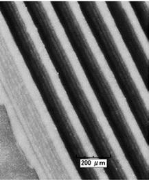
7 AJ Printed Copper Nanoink Circuit 20 μm line width Flip-chip pattern on 40 m thick flexible zirconia substrate

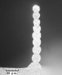
8 Aerosol Jet Printed Pillars 5mm standoff distance Student: Niranjan Damle 10mm standoff distance


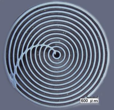
9 Microdispensing (nscrypt) Ink/Paste is dispensed through a needle valve Up to 1M cp Controllable Parameters Pressure Translation speed Valve position Dispensing height Nozzle diameter Multi-material dispensing?
10 Microextruded Fuel Cell Electrodes Student: Prasanna Khatri-Chhetri
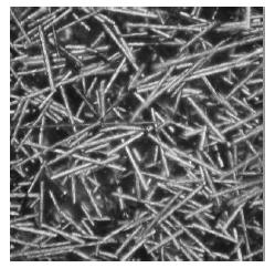
 Fibers align as they flow through the nozzle If proper feed and standoff are used, fibers maintain alignment as they exit the nozzle.")
11 Freeform Fiber Alignment Via Microextrusion Mix a UV curable epoxy with chopped carbon fibers Zoltek Panex 150 μm Pneumatically extrude the paste through a needle 22 gauge (~410 μm ID) Fibers align as they flow through the nozzle If proper feed and standoff are used, fibers maintain alignment as they exit the nozzle. Student: Chaitanya Mahajan

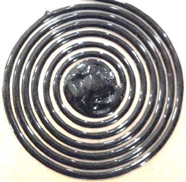
12 Toolpath Planning Fibers will align with the direction of nozzle travel Conventional raster filling patterns. Spiral patterns
13 Image Processing To Measure Fiber Alignment Student: Chaitanya Mahajan

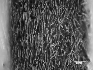
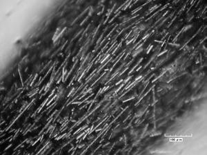

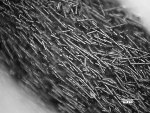

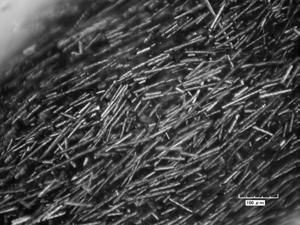
14 Student: Chaitanya Mahajan

15 Printed MEMS Drug Delivery Micropump

16 Pulsed Photonic Curing Rapid curing/sintering of high temperature printed materials (e.g. metal or ceramic) on low temperature surfaces (e.g. paper or plastic). Novacentrix pulsed photonic curing/sintering High power Xenon strobe lamps Peak Power: 100 kw/cm 2 Sustained Power: 5 MW/pulse Pulse Length: Down to 25 μsec Pulse Rate: Up to 1 khz Novacentrix Pulseforge 3300
17 Simplest Processing Condition: One Pulse Ag PET Conditions: Pulse length: 300 µs Radiant exposure: 1 J/cm 2 Stack: 1 µm Ag on 150 µm PET T [C] t [ms] High temperature processing removes excess solvent and enhances sintering. Substrate is undamaged. Novacentrix: Used with permission Numerical Simulation Peak surface temp >1000 C Substrate < ms Surface 20 micron from surface 150 micron from surface Thermal 35 ms (90C)

18 Micropulsing To convert the copper oxide to copper, certain elevated temperature must be reached and sustained long enough for the reaction to complete. The exact required temperature and time are not known a priori for a given system: too low or too high will yield poor results. Pulse Configurations Shaped Pulse (top) Basic Pulse (bottom) Resulting Thermal Simulation (Generated using SimPulse) This Basic Pulse creates temperature too hot and too short. Shaped Pulse creates optimal temperature for optimal time. Novacentrix: Used with permission


19 Pulsed Photonic Curing of Copper On Paper Copper oxide nanoink on paper Photonically cured copper nanoink


20 Photonic Curing of High Temperature Materials Yttria- Stabilized Zirconia Processing conditions 460V pulse for 250μs x 10 pulses at 2 Hz 10+ hrs in high temp furnace versus <1 sec in Pulseforge As-printed sample 1000X magnification Photonically sintered sample 1000X magnification

21 What About Photonic Curing With AM Processes? Broad spectrum Xenon flash lamps Interactions with polymer AM materials due to unwanted absorption? Novacentrix: Used with permission

22 Photonic Curing With Black ABS
23 Summary A variety of nano-ink printing processes are being used to produce micron-scale devices such as fuel cells, micropumps, and sensors Pulsed photonic curing is a promising approach for high speed curing/sintering of high temperature printed materials on low temperature substrates Opens up potential for printed electronics embedded on or within 3D printed geometries
24 Acknowledgments Support for portions of this work is gratefully acknowledged: Heterogeneous Functional Materials Center (HeteroFoam), an Energy Frontier Research Center (ERFC) funded by the U.S. Department of Energy and Office of Basic Energy Sciences under Award Number DE-SC NSF grant IIP Partnerships for Innovation in Printed Devices and Materials AFRL grant FA M-2259 for Low Temperature Processes for Ceramic Coated Heat Exchangers. Students Prasanna Khattri-Chettri, Sundar Balasubramanian, Anuj Datar, Niranjan Damle, Chaitanya Mahajan, Swaroop Yerasi, Arjun Wadhwa, Sourav Das, Akanksha Umrani, Pritam Poddar
Printed Electronics: Photonic Curing and Enabled Materials
 Printed Electronics: Photonic Curing and Enabled Materials Kurt Schroder, Dave Pope, Ian Rawson NovaCentrix 200-B Parker Dr Suite 580 Austin, TX 78728 Extended Abstract Introduction Photonic curing is
Photonic Drying Pulsed Light as a low Temperature Sintering Process
 Photonic Drying Pulsed Light as a low Temperature Sintering Process Lou Panico Xenon Corporation W E S T E R N M I C H I G A N U N I V E R S I T Y PRESENTATION OVERVIEW What is Printed Electronics Materials
LOW TEMPERATURE PHOTONIC SINTERING FOR PRINTED ELECTRONICS. Dr. Saad Ahmed XENON Corporation November 19, 2015
 LOW TEMPERATURE PHOTONIC SINTERING FOR PRINTED ELECTRONICS Dr. Saad Ahmed XENON Corporation November 19, 2015 Topics Introduction to Pulsed Light Photonic sintering for Printed Electronics R&D Tools for
3D inkjet printing of conductive structures using in-situ IR sintering
 3D inkjet printing of conductive structures using in-situ IR sintering E. Saleh*, J. Vaithilingam, C. Tuck, R. Wildman, I. Ashcroft, R. Hague, P. Dickens University of Nottingham, Additive Manufacturing
Advances in Intense Pulsed Light Solutions For Display Manufacturing. XENON Corporation Dr. Saad Ahmed Japan IDW 2016
 Advances in Intense Pulsed Light Solutions For Display Manufacturing XENON Corporation Dr. Saad Ahmed Japan IDW 2016 Talk Outline Introduction to Pulsed Light Applications in Display UV Curing Applications
Carbon Nanotube Solutions for Packaging and Wireless Sensors
 Carbon Nanotube Solutions for Packaging and Wireless Sensors Jim Lamb*, Liyong Diao, Christopher Landorf Jordan Valley Innovation Center (JVIC) Springfield, Missouri, USA *jlamb@brewerscience.com APEC
Advances in Printed Electronic Materials that Meet Cost and Performance Needs
 Advances in Printed Electronic Materials that Meet Cost and Performance Needs Mark S. Critzer DuPont Microcircuit Materials Research Triangle Park, NC mcm.dupont.com 1-800-284-3382 Agenda DuPont & Printed
Laser Micromachining - Market Focus. Dr. Andrew Kearsley
 Laser Micromachining - Market Focus Dr. Andrew Kearsley Oxford Lasers Ltd. Moorbrook Park, Didcot OX11 7HP andrew.kearsley@oxfordlasers.com 5th CIR HVM-UK: South East Conference Harwell, 17 November 2005
Advances in Printing nano Cu and Using Existing Cu Based Manufacturing Processes. Michael J. Carmody Chief Scientist, Intrinsiq Materials
 Advances in Printing nano Cu and Using Existing Cu Based Manufacturing Processes Michael J. Carmody Chief Scientist, Intrinsiq Materials Why Use Copper? Lower Cost than Silver. Print on Numerous Substrates.
Die Attach Materials. Die Attach G, TECH. 2U. TECHNICAL R&D DIV.
 Die Attach Materials Die Attach G, TECH. 2U. TECHNICAL R&D DIV. 2 Topics 3 What it is X 5,000 X 10,000 X 50,000 Si Chip Au Plating Substrate Ag Resin 4 Current Products Characteristics H9890-6A H9890-6S
TECHNOLOGIES FOR APPLYING FLUIDS IN SEMICONDUCTOR PACKAGING
 TECHNOLOGIES FOR APPLYING FLUIDS IN SEMICONDUCTOR PACKAGING Alec J. Babiarz Asymtek Carlsbad, CA, USA ajbabiarz@asymtek.com ABSTRACT Jetting fluids in semiconductor packaging and assembly has become an
High Speed Sintering for 3D printing applications
 High Speed Sintering for 3D printing applications High Speed Sintering for 3D printing applications Neil Hopkinson, Adam Ellis, Adam Strevens, Manolis Papastavrou and Torben Lange, Xaar plc Introduction
Aqueous-Based Extrusion Fabrication of Ceramics on Demand
 Aqueous-Based Extrusion Fabrication of Ceramics on Demand Michael S. Mason 1, Tieshu Huang 1, Robert G. Landers 1, Ming C. Leu 1, Gregory E. Hilmas 2, and Michael W. Hayes 3 1870 Miner Circle Department
Photonic Sintering of Silver for Roll-to-Roll Printed Electronics. Saad Ahmed, PhD Manager-Engineering
 Photonic Sintering of Silver for Roll-to-Roll Printed Electronics Saad Ahmed, PhD Manager-Engineering Topics Introduction Significance of nanotechnology Conductive inks Pulsed light for sintering Reel-to-reel
Aerosol Jet International User Group Meeting. Metallization and Functional Structures by Aerosol Jet deposition
 17.10.2012 1 2012 Aerosol Jet International User Group Meeting Metallization and Functional Structures by Aerosol Jet deposition Andreas Brose Institut für Mikro- und Sensorsysteme Lehrstuhl Mikrosystemtechnik
Roll-to-roll Vacuum Processing of Organic Thin Film Transistors
 Roll-to-roll Vacuum Processing of Organic Thin Film Transistors Hazel Assender Department of Materials University of Oxford DALMATIAN TECHNOLOGY 1 Aim of the Research To demonstrate the ability to fabricate
HVM Graphene Conference Oxford, UK 15 May uk.com
 HVM Graphene+ 2014 Conference Oxford, UK 15 May www.hvm- uk.com Electronic inks and pastes for packaging, ba4eries, sensors, displays and touchscreens Dr Paul Reip Founder & Director, Government and Strategic
Plastics for Additive Manufacturing
 Sources: voxeljet, Materialise NV, Iris van Herpen Plastics for Additive Manufacturing Dr. Thomas Büsgen Bayer MaterialScience AG 20 th November 2013, 3D Printing & Additive Manufacturing Industrial Applications
Dicing Glass Optical Devices
 Glass Applications Dicing Glass Optical Devices -Blade Characteristics 2,, 4 4 Resin Type Q Diamond grit size: 15-45 mic. Thickness: 0.006-0.012 0.012 (0.15mm 0.3mm) Metal Sintered E08 & New matrices 8-258
Studies on Atmospheric Non-Thermal Plasma Jet Device
 Int. J. New. Hor. Phys. 3, No. 1, 1-6 (2016) 1 International Journal of New Horizons in Physics http://dx.doi.org/10.18576/ijnhp/030101 Studies on Atmospheric Non-Thermal Plasma Jet Device H. A. El-sayed*,
High Throughput Laser Processing of Guide Plates for Vertical Probe Cards Rouzbeh Sarrafi, Dana Sercel, Sean Dennigan, Joshua Stearns, Marco Mendes
 High Throughput Laser Processing of Guide Plates for Vertical Probe Cards Rouzbeh Sarrafi, Dana Sercel, Sean Dennigan, Joshua Stearns, Marco Mendes IPG Photonics - Microsystems Division Outline Introduction
Proceedings Aerosol/Ink Jet Printing Technology for High-Temperature MEMS Sensors
 Proceedings Aerosol/Ink Jet Printing Technology for High-Temperature MEMS Sensors Alexey A. Vasiliev 1,2,*, Anton V. Nisan 3 and Nikolay N. Samotaev 4 1 Kurchatov Complex of Physical and Chemical Technologies,
Smartphone with compact camera. Compact Camera Module Assembly Customized Adhesives
 Compact Camera Module Assembly Customized Adhesives Smartphone with compact camera module assembly Perfection is our goal That is why we have developed a wide range of highquality adhesives to answer the
Challenges for Embedded Device Technologies for Package Level Integration
 Challenges for Embedded Device Technologies for Package Level Integration Kevin Cannon, Steve Riches Tribus-D Ltd Guangbin Dou, Andrew Holmes Imperial College London Embedded Die Technology IMAPS-UK/NMI
Fraunhofer ENAS Current results and future approaches in Wafer-level-packaging FRANK ROSCHER
 Fraunhofer ENAS - Current results and future approaches in Wafer-level-packaging FRANK ROSCHER Fraunhofer ENAS Chemnitz System Packaging Page 1 System Packaging Outline: Wafer level packaging for MEMS
Laser assisted Cold Spray
 2009-02-16 Laser assisted Cold Spray Andrew Cockburn, Matthew Bray, Rocco Lupoi Bill O Neill Innovative Manufacturing Research Centre (IMRC) Institute for Manufacturing, Department of Engineering, University
An Innovative High Throughput Thermal Compression Bonding Process
 An Innovative High Throughput Thermal Compression Bonding Process Li Ming 2 September 2015 Outline Introduction Throughput improved TCB Process Liquid Phase Contact (LPC) bonding Flux-LPC-TCB under inert
OPTIMISED CURING OF SILVER INK JET BASED PRINTED TRACES
 Nice, Côte d Azur, France, 27-29 September 2006 OPTIMISED CURING OF SILVER INK JET BASED PRINTED TRACES Z. Radivojevic 1, K. Andersson 1, K. Hashizume 2, M. Heino 1, M. Mantysalo 3, P. Mansikkamaki 3,
THE ASPECTS ABOUT RAPID PROTOTYPING SYSTEM
 THE ASPECTS ABOUT RAPID PROTOTYPING SYSTEM Adrian P. POP 1, Petru UNGUR 1, Gheorghe BEJINARU MIHOC 2 1 University of Oradea, e-mail: adippop@yahoo.com; petru_ungur@yahoo.com; 2 Transilvania University
Hitachi Anisotropic Conductive Film ANISOLM AC-8955YW. Issued 2007/03/30
 Hitachi Chemical Data Sheet Hitachi Anisotropic Conductive Film ANISOLM AC-8955YW Issued 27/3/3 1. Standard specification, bonding condition, storage condition and characteristic...1 2. Precautions in
Enhanced Piezoelectric Performance of Printed PZT Films on Low Temperature Substrates
 Rochester Institute of Technology RIT Scholar Works Theses Thesis/Dissertation Collections 8-2-2017 Enhanced Piezoelectric Performance of Printed PZT Films on Low Temperature Substrates Jing Ouyang jxo7115@rit.edu
Features Conductive Room Temperature Cure. Product Ref IP 4525IP Low viscosity adhesive & coating. High thermal conductivity
 Properties and Part Selection Overview Selection Table - Epoxy-Based Adhesive Properties Features Conductive Room Temperature Cure Product Ref 120 132 4461IP 42IP 438 700 Properties High electrical conductivity
A New Thermal Management Material for HBLEDs based on Aluminum Nitride Ceramics
 A New Thermal Management Material for HBLEDs based on Aluminum Nitride Ceramics Thermal Management Challenges in HBLED Excess heat leads to a whole range of performance and reliability issues for high
HIGH TEMPERATURE CERAMIC & GRAPHITE ADHESIVES
 HIGH TEMPERATURE & GRAPHITE S Technical Bulletin A2 Ceramabond 835-M bonds halogen lamp. Ceramabond 503 coats heater used to 1700 ºC. Ceramabond 685-N bonds infrared heater. Graphi-Bond 551-RN bonds graphite
Enhanced Response from Engineered Nano Treated Peizofilm
 Enhanced Response from Engineered Nano Treated Peizofilm By Sai Narayan Sundar Advisor Dr J.P Sharma Dept. of Mechanical Engineering University of Mississippi i: flow of current due to piezo deformation
Photolithography I ( Part 2 )
") 1 Photolithography I ( Part 2 ) Chapter 13 : Semiconductor Manufacturing Technology by M. Quirk & J. Serda Bjørn-Ove Fimland, Department of Electronics and Telecommunication, Norwegian University of Science
1 Photolithography I ( Part 2 ) Chapter 13 : Semiconductor Manufacturing Technology by M. Quirk & J. Serda Bjørn-Ove Fimland, Department of Electronics and Telecommunication, Norwegian University of Science
Liquid Optically Clear Adhesive for Display Applications
 Liquid Optically Clear Adhesive for Display Applications Daniel Lu, PhD Technical Director Henkel Corporation LOCTITE Liquid Optically Clear Adhesives (LOCA) Cover lens LOCA Touch sensor LOCA LCD 2 LOCA
MRSI-175Ag Epoxy Dispenser
 MRSI-175Ag Epoxy Dispenser Applications: Microwave & RF Modules MEMS Semiconductor Packaging Multi-Chip Modules Hybrid Circuits Optical Modules Overview The MRSI-175Ag Conductive Epoxy Dispenser handles
Alternative Methods of Yttria Deposition For Semiconductor Applications. Rajan Bamola Paul Robinson
 Alternative Methods of Yttria Deposition For Semiconductor Applications Rajan Bamola Paul Robinson Origin of Productivity Losses in Etch Process Aggressive corrosive/erosive plasma used for etch Corrosion/erosion
Ultralow Residue Semiconductor Grade Fluxes for Copper Pillar Flip-Chip
 Ultralow Residue Semiconductor Grade Fluxes for Copper Pillar Flip-Chip SzePei Lim (Presenter), Jason Chou, Maria Durham, and Dr. Andy Mackie Indium Corporation 1 Outline of Presentation Roadmaps and challenges
Optimizing the Assembly Process with Cure-On-Demand UV/Visible Light-Curable Adhesives
 Optimizing the Assembly Process with Cure-On-Demand UV/Visible Light-Curable Adhesives Virginia P. Read Industrial Market Segment Manager DYMAX Corporation Torrington, CT www.dymax.com Introduction Manufacturers
TSV Processing and Wafer Stacking. Kathy Cook and Maggie Zoberbier, 3D Business Development
 TSV Processing and Wafer Stacking Kathy Cook and Maggie Zoberbier, 3D Business Development Outline Why 3D Integration? TSV Process Variations Lithography Process Results Stacking Technology Wafer Bonding
Technical Data Sheet Effective: 17/6/16 Supersedes: 29/10/99
 Automotive Aftermarket Division 3M 08115 Panel Bonding Adhesive 1) Part Numbers 3M 08115 : 200ml Duo Pack cartridges (2/1 ratio by volume) Applicators: 3M 08117 3M 09930 : Manual applicator gun : Pneumatic
Multiphoton lithography based 3D micro/nano printing Dr Qin Hu
 Multiphoton lithography based 3D micro/nano printing Dr Qin Hu EPSRC Centre for Innovative Manufacturing in Additive Manufacturing University of Nottingham Multiphoton lithography Also known as direct
Adhesives, Sealants, Equipment and Services. Water, Food and Beverage Filtration Solutions Medical Filtration Solutions
 Adhesives, Sealants, Equipment and Services Water, Food and Beverage Filtration Solutions Medical Filtration Solutions 2 Filtration Solutions for Water, Food and Beverage, Medical 1-800-562-8483 www.henkelna.com/filters
Laser Sintering of Silver Ink for Generation of Embedded Electronic Circuits in Stereolithography Parts
 Lasers in Manufacturing Conference 2015 Laser Sintering of Silver Ink for Generation of Embedded Electronic Circuits in Stereolithography Parts Bernd Niese a *, Uwe Urmoneit a, Philipp Amend a, Stephan
Transition Temperature Microscopy Nano-scale Thermal Analysis Technique
 Transition Temperature Microscopy Nano-scale Thermal Analysis Technique Khoren Sahagian Anasys Instruments Steven Goodman 10H Technology Inc. 2010 Anasys Instru Outline Introduction to Nano Thermal Analysis
Selection and Application of Board Level Underfill Materials
 Selection and Application of Board Level Underfill Materials Developed by the Underfill Materials Design, Selection and Process Task Group (5-24f) of the Assembly and Joining Committee (5-20) of IPC Supersedes:
Evaluation of Aerosol Jet Printing (AJP) technology for electronic packaging and interconnect technique
 technology for electronic packaging and interconnect technique") Evaluation of Aerosol Jet Printing (AJP) technology for electronic packaging and interconnect technique S. Stoukatch a, P. Laurent a, S. Dricot a, F. Axisa a, L.Seronveaux b, D.Vandormael b, E.Beeckman
Evaluation of Aerosol Jet Printing (AJP) technology for electronic packaging and interconnect technique S. Stoukatch a, P. Laurent a, S. Dricot a, F. Axisa a, L.Seronveaux b, D.Vandormael b, E.Beeckman
Hot Pin Pull Method New Test Procedure for the Adhesion Measurement for 3D-MID
 Hot Pin Pull Method New Test Procedure for the Adhesion Measurement for 3D-MID HARTING Mitronics Christian Goth in cooperation with: FAPS Thomas Kuhn, Gerald Gion, Jörg Franke 11 th International Congress
New Developments in Moisture Barrier Materials and Conductive Adhesives for Flexible Display Applications
 T H E C U S T O M E R F O C U S E D E L E C T R O N I C S O L U T I O N P R O V I D E R New Developments in Moisture Barrier Materials and Conductive Adhesives for Flexible Display Applications Dr. Stijn
Crossflow Filtration for Ink Jet Fluids
 Crossflow Filtration for Ink Jet Fluids For ink jet ink and colorant formulation, efficient filtration makes all the difference. Improve your process and product with crossflow technology. In recent years,
Chapter 3 Silicon Device Fabrication Technology
 Chapter 3 Silicon Device Fabrication Technology Over 10 15 transistors (or 100,000 for every person in the world) are manufactured every year. VLSI (Very Large Scale Integration) ULSI (Ultra Large Scale
Basic PCB Level Assembly Process Methodology for 3D Package-on-Package
 Basic PCB Level Assembly Process Methodology for 3D Package-on-Package Vern Solberg STC-Madison Madison, Wisconsin USA Abstract The motivation for developing higher density IC packaging continues to be
Flexible functional devices at mass production level with the FLEx R2R sald platform
 Flexible functional devices at mass production level with the FLEx R2R sald platform D. Spee, W. Boonen, D. Borsa and E. Clerkx Meyer Burger (Netherlands) B.V. Meyer Burger Introduction to sald Challenges
Barix Multilayers: a Water and Oxygen Barrier for Flexible Organic Electronics. Robert Jan Visser
 Barix Multilayers: a Water and Oxygen Barrier for Flexible Organic Electronics Robert Jan Visser Organic Electronics Is the Future of Electronics Organic? MIT Stanford UC Berkeley Nano Forum Vitex Systems,
Freshure Coatings: Environmentally Friendly Barrier Coatings
 Freshure Coatings: Environmentally Friendly Barrier Coatings Shahab Jahromi Knowfort Technologies BV Urmonderbaan 20a 6160MD Geleen The Netherlands Email: s.jahromi@knowfort.com Introduction. Roll-to-roll
Polymer-based optical interconnects using nano-imprint lithography
 Polymer-based optical interconnects using nano-imprint lithography Arjen Boersma,Sjoukje Wiegersma Bert Jan Offrein, Jeroen Duis, Jos Delis, Markus Ortsiefer, Geert van Steenberge, MikkoKarppinen, Alfons
HiPIMS Deposition of Metal and Oxide Coatings
 HiPIMS Deposition of Metal and Oxide Coatings 1 GT West, 1 PJ Kelly, 1 P Barker, 2 JW Bradley and 2 A Mishra 1. Surface Engineering Group, Manchester Metropolitan University, UK 2. Electrical Engineering
Application of Electronic Devices for Aerosol Deposition Methods
 Application of Electronic Devices for Aerosol Deposition Methods NAKADA Masafumi, KAWAKAMI Toshihiro, IWANAMI Mizuki, OHASHI Keishi Abstract Oxide materials have superior functional characteristics that
UV Coloring of Optical Fiber Final Report
 UV Coloring of Optical Fiber Final Report Why Change the Process? Alcatel Telecommunications Cable located in Claremont, North Carolina, manufactures optical fiber and cable. After fiber is produced, it
DATA SHEET A5000 RELEASE FILM
 A5000 RELEASE FILM HAWKEYE A5000 RELEASE FILM is a high temperature release film which lends itself readily to overcome bridging in contour layups. With more elongation than the HK3760 or nylon films,
KGC SCIENTIFIC Making of a Chip
 KGC SCIENTIFIC www.kgcscientific.com Making of a Chip FROM THE SAND TO THE PACKAGE, A DIAGRAM TO UNDERSTAND HOW CPU IS MADE? Sand CPU CHAIN ANALYSIS OF SEMICONDUCTOR Material for manufacturing process
Fig1: Melt pool size of LAMP vs. µlamp. The LAMP process s melt pool is x the area of the LAMP s melt pool.
 Proceedings of the 4th Annual ISC Research Symposium ISCRS 2010 April 21, 2010, Rolla, Missouri LOW COST IMAGING OF MELTPOOL IN MICRO LASER AIDED MANUFACTURING PROCESS (µlamp) ABSTRACT This paper describes
3D Laser Metal Sintering System
 \ 3D Laser Metal Sintering System FONON TECHNOLOGIES F O N O N 3 D M E T A L P R I N T I N G S Y S T E M S 3D FUSION - NANO Powder Direct Metal Sintering System Fonon Additive Manufacturing Technologies
Development of Novel NOx Sensors and System Integration with Alumina Heater Elements
 Development of Novel NOx Sensors and System Integration with Alumina Heater Elements UC Riverside PEMS 2016 International Conference & Workshop March 17, 2016 F. Bell, M. Boettcher, J. Chee, J. Fitzpatrick,
3 Pulsed laser ablation and etching of fused silica
 3 Pulsed laser ablation and etching of fused silica 17 3 Pulsed laser ablation and etching of fused silica Material erosion caused by short laser pulses takes place far from equilibrium and may be based
Nanoimprinting in Polymers and Applications in Cell Studies. Albert F. YEE Chemical Engineering & Materials Science UC Irvine
 Nanoimprinting in Polymers and Applications in Cell Studies Albert F. YEE Chemical Engineering & Materials Science UC Irvine Presentation outline Motivation Reversal imprinting Soft inkpad imprinting on
Fabrication of Low Adhesion Films Through Pulsed Light Sintering
 Rochester Institute of Technology RIT Scholar Works Theses Thesis/Dissertation Collections 2-24-2017 Fabrication of Low Adhesion Films Through Pulsed Light Sintering Dhananjay Dubey dd1668@rit.edu Follow
PH Electrode. Application. General lab and field use. For viscous solutions and lab use. For viscous solutions. General lab and field use
 PH Electrode Model PH Combined Electrode with Glass Body Application 65-IP General lab and field use 65-IIP 65-IA 65-IIA For viscous solutions and lab use For viscous solutions PH Combined Electrode with
Enhancing the Performance & Reliability of Your Electronics Designs. Innovative Thermally Conductive Silicone Solutions IMAGINE
 Enhancing the Performance & Reliability of Your Electronics Designs Innovative Thermally Conductive Silicone Solutions IMAGINE Heat Is the Enemy of Electronic Devices The reasons why may vary from application
Supporting Information. Self-Supporting Nanoclay as Internal Scaffold Material for Direct Printing of Soft Hydrogel Composite Structures in Air
 Supporting Information Self-Supporting Nanoclay as Internal Scaffold Material for Direct Printing of Soft Hydrogel Composite Structures in Air Yifei Jin 1, Chengcheng Liu 2, Wenxuan Chai 1, Ashley Compaan
Smart materials. Piezoelectric materials Shape memory materials Magnetostriction materials Electrostriction materials. w.wang 107
 Smart materials Piezoelectric materials Shape memory materials Magnetostriction materials Electrostriction materials w.wang 107 Qualitative comparison of different smart technology Active System Driving
Carbon film resistors
 Carbon film resistors (6.3 φ 2.4 size: 1 / 3W) ROHM resistors are produced using an integrated production system for parts and materials, and state of the art technology to ensure high precision productivity,
Atomic Oxygen-Resistant, Static-Dissipative, Pinhole-Free Coatings for Spacecraft
 Physical Sciences Inc. VG10-109 Atomic Oxygen-Resistant, Static-Dissipative, Pinhole-Free Coatings for Spacecraft Michelle T. Schulberg, Robert H. Krech, Frederick S. Lauten Physical Sciences Inc. Roy
Experiences of PLD Technology for LIB Separators. PICODEON Oy. Neal White
 Experiences of PLD Technology for LIB Separators PICODEON Oy Neal White 1 Outline Introduction to Picodeon Ceramic coating rationale Separator overview Why PLD for LIB separators Current status of Picodeon
Scotch-Weld Metal Bonder Acrylic Adhesive DP8407NS Gray
 Scotch-Weld Metal Bonder Acrylic Adhesive Preliminary Technical Data Sheet October 2017 Product Description is a high performance, two-part acrylic adhesive that offers excellent shear, peel, and impact
Large-area laser-lift-off processing in microelectronics
 Available online at www.sciencedirect.com Physics Procedia 41 (2013 ) 241 248 Lasers in Manufacturing Conference 2013 Large-area laser-lift-off processing in microelectronics R. Delmdahl*, R. Pätzel, J.
MATHEMATICAL MODELING OF DRYING KINETICS OF CORN IN ELECTRON FIRED FLUIDIZED BED DRYER
 International Journal of Mechanical Engineering and Technology (IJMET) Volume 8, Issue 6, June 2017, pp. 51 58, Article ID: IJMET_08_06_006 Available online at http://www.iaeme.com/ijmet/issues.asp?jtype=ijmet&vtype=8&itype=6
Innovative, Thermally Conductive Silicone Solutions for LED Lighting
 Innovative, Silicone Solutions for LED Lighting Better Performance and Reliability for your Lighting Designs With Dow Corning, You Have a Powerful Ally for Thermal Management Heat remains the enemy of
High Efficiency UV LEDs Enabled by Next Generation Substrates. Whitepaper
 High Efficiency UV LEDs Enabled by Next Generation Substrates Whitepaper Introduction A primary industrial market for high power ultra-violet (UV) LED modules is curing equipment used for drying paints,
HIGH TEMPERATURE CERAMIC ADHESIVES & PASTES
 HIGH TEMPERATURE CERAMIC ADHESIVES & PASTES Technical Bulletin A A Aremco s high temperature ceramic adhesives are unique inorganic formulations for bonding and sealing ceramics, metals, quartz, graphites,
Introduction of CSC Pastes
 Introduction of CSC Pastes Smart Phones & Conductive Pastes Chip Varistors Chip Inductors LC Filters Flexible Printed Circuit Boards Electronic Molding Compounds ITO Electrodes PCB Through Holes Semiconductor
IMRE/ETPL Flagship Project
 IMRE/ETPL Flagship Project Nanoparticulate Barrier Films & Gas Permeation Measurement Techniques for Thin Film Solar & Display Application Problems Senthil Ramadas Institute of Materials Research & Engineering
for Dye Sensitized Solar Cells.
 Supporting Information Copper Phenanthroline as Fast and High Performance Redox Mediator for Dye Sensitized Solar Cells. Marina Freitag *, Fabrizio Giordano #, Wenxing Yang, Meysam Pazoki, Yan Hao, Burkhard
Hydrodynamics of Drop Impact and Spray Cooling through Nanofiber Mats
 Hydrodynamics of Drop Impact and Spray Cooling through Nanofiber Mats Y. Chan Department of Chemical Engineering, University of Massachusetts Amherst, Amherst, MA 01003 F. Charbel Department of Mechanical
PARYLENE ENGINEERING. For Longer Lasting Products
 PARYLENE ENGINEERING For Longer Lasting Products PARYLENE ENGINEERING This presentation serves as a quick overview of the conformal coating material and processes currently used in the industry. The field
Overview Ablating Cutting Drilling Welding Boston Costa Rica Dayton San Diego
 Overview Ablating Cutting Drilling Welding Boston Costa Rica Dayton San Diego Who is Resonetics? Mission Resonetics will be the leader in laser micro manufacturing for the life sciences industry by providing
CIA-GEL 7000 EPOXY. One Product For All Applications ADHESIVE ANCHORING SYSTEMS FOR CONCRETE AND MASONRY
 CIA-GEL 000 EPOXY One Product For All Applications ADHESIVE ANCHORING SYSTEMS FOR CONCRETE AND MASONRY City of Los Angeles Research Report No. (in Concrete, Block and Brick) City of Los Angeles Research
ITO SPUTTER COATED FILMS FOR TOUCH PANEL APPLICATIONS USING ROTARY SINTERED CERAMIC ITO TARGETS: WHAT CAN BE LEARNED FROM GLASS COATING?
 ITO SPUTTER COATED FILMS FOR TOUCH PANEL APPLICATIONS USING ROTARY SINTERED CERAMIC ITO TARGETS: WHAT CAN BE LEARNED FROM GLASS COATING? Paul Lippens AIMCAL Web coating conference 2012 Outline Introduction
Product Bulletin 2K-3.2. stamixco. mix it up..
 stamixco Product Bulletin 2K-3.2 mix it up.. 2-Component Resin Mixing Technology Plastic Disposable & Metal Static Mixers for Mixing Viscous Materials 2 Introduction For more than 40 years, static mixers
NTT-AT Optical Adhesives Lineup. Adhesives / Resins and Sealants for Optical Component Assembly
 NTT-AT Optical Adhesives Lineup Adhesives / Resins and Sealants for Optical Component Assembly The adhesive technology used in optical communications is one of the key technologies we offer. Ask us anything
Reference Only. 2.Part Numbering (ex) NF Z 5B BW 2R9 L N 1 0 L
 NF Z 5B BW 2R9 L N 1 0 L") SpecNo.JENF243J-0011A-01 P1/10 CHIP NOISE FILTER NFZ5BBW LN10 REFERENCE SPECIFICATION 1.Scope This reference specification applies to NFZ5BBW_LN10L Series, Chip Noise Filter. 2.Part Numbering (ex) NF Z
SpecNo.JENF243J-0011A-01 P1/10 CHIP NOISE FILTER NFZ5BBW LN10 REFERENCE SPECIFICATION 1.Scope This reference specification applies to NFZ5BBW_LN10L Series, Chip Noise Filter. 2.Part Numbering (ex) NF Z
Reference Only. Spec. No. JENF243D-0006K-01 P 1/ 8
 Spec. No. JENF243D-0006K-01 P 1/ 8 Chip EMIFIL LC Combined Monolithic NFL21SP X1C Reference Specification 1. Scope This reference specification applies to Chip EMIFIL LC Combined Monolithic Type NFL21S
INDUSTRIAL FILTRATION EQUIPMENT LWS Filter Series
 INDUSTRIAL FILTRATION EQUIPMENT LWS Filter Series (Single, Twin, Triple or Quadruple Demand Systems) 1 P age filtration equipment can be engineered to solve complex commercial and industrial water treatment
PEC (Printed Electronic Circuit) process for LED interconnection
 process for LED interconnection") PEC (Printed Electronic Circuit) process for LED interconnection Higher wattage LED s/ power components or their placement in higher densities, requires a larger dissipation of heat in a more effective
PEC (Printed Electronic Circuit) process for LED interconnection Higher wattage LED s/ power components or their placement in higher densities, requires a larger dissipation of heat in a more effective
With the influx of plastic
 UV-Curable Basecoats and Clearcoats for Automotive Lighting By Eileen Weber and Phil Abell With the influx of plastic into automotive lighting in the early 198s, a fresh market for coatings quickly emerged.
Lecture 10: MultiUser MEMS Process (MUMPS)
") MEMS: Fabrication Lecture 10: MultiUser MEMS Process (MUMPS) Prasanna S. Gandhi Assistant Professor, Department of Mechanical Engineering, Indian Institute of Technology, Bombay, 1 Recap Various VLSI based
MEMS: Fabrication Lecture 10: MultiUser MEMS Process (MUMPS) Prasanna S. Gandhi Assistant Professor, Department of Mechanical Engineering, Indian Institute of Technology, Bombay, 1 Recap Various VLSI based
Woven Electrodes for Optoelectronic Devices. Peter Chabrecek. Sefar AG, 9425 Thal, Switzerland
 Peter Chabrecek Sefar AG, 9425 Thal, Switzerland Actual SEFAR business Sefar's core skills is the manufacture and market of fabrics with precise mesh openings for screen printing and filtration processes
Scotch-Weld Acrylic Adhesives
 Scotch-Weld Acrylic Adhesives Technical Data Sheet October 2016 Product Description s are high performance, two-part acrylic adhesives that offer excellent shear, peel, and impact performance. These toughened