Conductive Paste-Based Interconnection Technology for High Performance Probe Card
|
|
|
- Edwina Wilkinson
- 6 years ago
- Views:
Transcription


1 Conductive Paste-Based Interconnection Technology for High Performance Probe Card Sang-il Kwon Eddy Kang TSE Co., Ltd.
2 Overview Introduction of TABP Technology Key Technology of Core to Core Interconnection Test Results & Application Examples Electrical & Thermal Reliability of Core to Core Interconnection PCB by Actual Application Probe Card Application by Design Rules Conclusions 2


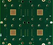

3 Who we are TSE Co., Ltd. Probe Card Load Board Affiliated Companies Memory Test Board Test Socket 3

4 What is TABP? TABP = TSE Advanced Bump PCB Core to core interconnection PCB Before After Core Pad Bismuth Tin Sintered Copper/Tin Alloy Metal Network Copper Liquid Organic Formulation Core Pad <Structural Change of Conductive Paste by Sintering> Electrical Interconnection <Section View> 4


5 Advantages of TABP Free of Thick Board Drilling Free of High Aspect Ratio Via Hole Plating Reducing Complexity of Back Drilling Enhance Fabrication Capability for Fine Pitch HDI PCBs IST Coupon Layup Structure Cross Section L01 L09 1.5mm - Min. Pitch : 0.4mm -Layer Count: 34 - Thickness : 6.4mm - Aspect Ratio : Via Size : 0.125mmΦ - PCB Size : 12.7mm x 50.8mm A/R: 12 A/R: 51.2 L10 L17 L18 L25 L26 L34 6.4mm 1.5mm 1.5mm 1.5mm 5
6 TABP Fabrication Process Flow Prepreg Tacking Type Tacking Laser Drill Paste Filling Remove PET CORE Hot Press PET PP PET PET PP PET PET PP PP PP PET Conductive Paste Pocket Conductive Paste CORE Core & Prepreg Tacking Type Tacking Laser Drill Paste Filling Remove PET Hot Press PET PP CORE PET PP CORE Conductive Paste Pocket PET PP CORE Conductive Paste PP CORE CORE PP CORE 6
7 Key Technology TABP Electrical Conductivity (TSE Advanced Bump PCB) Thermal Reliability Perfect Sintered Alloy Structure Sufficient Amount of Paste Fill Optimized Forming of Conductive Paste Pocket Withstanding Thermal Stress Sintered Alloy Bonding Layer Sufficient Resin at Bonding Layer Optimized Material, Layup & Design 7

 0.5mm Max. 6.0Ω 6.65mΩ (12DUTs) Min. 5.64Ω 4.64mΩ 0.4mm Max. 7.63Ω 7.05mΩ (12DUTs) Min. 7.25Ω 4.")
8 Electrical Conductivity Coupon Board - 0.5mm Pitch 12DUTs & 0.4mm Pitch 12DUTs - Each Via has 1 TABP interconnection. - BGA Count of Each DUT = 1,024 - Each Via in Same DUT connected by Daisy Chain - PCB Thickness = 1.2mm DC Interconnection Resistance Values Daisy Chained DUT Each BGA Via BGA Pitch (1,024 BGA 24DUTs) (Total Count=24,576Ea) 0.5mm Max. 6.0Ω 6.65mΩ (12DUTs) Min. 5.64Ω 4.64mΩ 0.4mm Max. 7.63Ω 7.05mΩ (12DUTs) Min. 7.25Ω 4.81mΩ Measured by DVM, Microcraft EMX6151 8


9 Electrical Conductivity Hole Resistance (mω) Via Holes Resistance of 1 DUT Cross Section of Test Coupon BGA Pitch : 0.4mm - 1,024 TABP Vias in 1DUT - Max Via Hole resistance : 7.05mΩ - Laser Drill Diameter : 150μm - Prepreg Thickness : 110μm <Stable Sintered Alloy Structure> 9


10 Thermal Reliability Cross Section Analysis after Solder Pot Floating Test - Thermal Impact Condition : 3 Times, 288 C Solder Pot Floating 10sec - BGA Count per Each DUT : 100, 600, 1024 & 1600 Ea - Each Via in Same DUT connected by Daisy Chain - All BGA Interconnection Test was passed. - TABP can withstand Thermal Impact of Solder Floating Test. After Lamination After Out Layer Formation After Printing All passed after 3X T/I All passed after 3X T/I All passed after 3X T/I 10
11 Thermal Reliability Resistance Changes after Solder Reflow Exposures - Reflow Condition : 6 Times C - BGA Count per Each DUT : 100, 600, 1024 & 1600 Ea - Each Via in Same DUT connected by Daisy Chain - All BGA Interconnection Test was passed. - IPC Standards for DC Resistance Change after Reflow : Max 10% 10 % 5 % 0 % -5 % -10 % 10 % 5 % 0 % -5 % -10 % Resistance Change of 100BGA reflow 6 time 5.56 Hole Hole Hole Hole Resistance Change of 1024BGA reflow 6 time 0.36 Hole Hole Hole Hole % 5 % 0 % -5 % -10 % 10 % 5 % 0 % -5 % -10 % Resistance Change of 600BGA reflow 6 time Hole Hole Hole Hole Resistance Change of 1600BGA reflow 6 time 3.97 Hole Hole Hole Hole


12 Thermal Reliability Cross Section Analysis after 6x Reflow Exposure - Board Profile : 296FBGA, 0.35mm Pitch, 4mmT, 3 TABP, 0.15mmΦ Laser Drill - Applied Thermal Impact Condition : 6 Times C - TABP s Structural Stability can withstand 6 times of Reflow Condition. < Cross Section after Thermal Impact> Stable Paste Structure & Bonding Condition 12

 0.")
13 TABP Application Examples Load Board 0.4mm Pitch, Aspect Ratio 41.3 Board Profiles - BGA Pitch : 0.4mm Pitch - Layer Count : 38L - Thickness : 6.2mm - Via Size : 0.15mmΦ - Aspect Ratio : PCB Size : 340mm x 520mm - Option : TABP + HPL + Back Drill Structure (BGA) 0.4mmP (BGA) 0.4mmP 6.2mm 0.125Φ 0.15Φ Cross Section Unnecessary Stubs Reduced 13


14 TABP Application Examples Memory Test Board 0.35mm Pitch, Aspect Ratio 28 Board Profiles Structure Cross Section - BGA Pitch : 0.35mm - Layer count : 38 - Thickness : 3.5mm - Via Size : 0.125mmΦ - Aspect Ratio : 28 - PCB Size : 59mm x 109 mm - Option : TABP + HPL + Back Drill 14


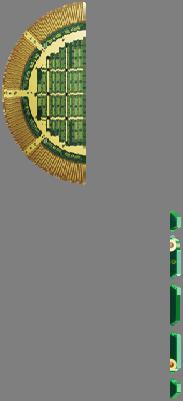
15 TABP Application Examples Pretest Coupon - 0.3mm Pitch, Aspect Ratio 62 Board Profiles - BGA Pitch : 0.3mm - Layer Count : 34 - Thickness : 6.2mm - Via Size : 0.1mmΦ - Aspect Ratio : 62 - PCB Size : 26mm x 26mm - Option : TABP + HPL + Back Drill Structure Cross Section L01 L09 L10 L17 6.2mm L18 L25 L26 L34 15
16 Challenges for Probe Card PCB High Layer Count / High Aspect Ratio SI Performance for High Speed Application Design/Fabricate PCB at Competitive Conditions TABP is a Solution for Advanced Probe Card PCB. by Eliminating of Thick Board Drilling by Eliminating of High Aspect Ratio Via Plating by Reducing Drilling Complexity & Improving Yield 16
17 Design Rule for 0.8mm Pitch P/C PCB 0.8P 0.8P in Double Line Array Plating Through Hole Type DRILL A LAND 6.2mm CLEAR C B 0.25Φ Drill Dia. A/R Line Width A B C Land to Line Line to Line Drill to Metal 250μmΦ μm 80μm 80μm 155μm 17
18 Design Rule for 0.8mm Pitch P/C PCB TABP Type 0.8P 0.8P 0.8P 2.06mm in Double Line Array DRILL LAND A 2.06mm 6.2mm TABP CLEAR C B 2.06mm 0.125Φ Drill Dia. A/R Line Width 125μmΦ 49.6 (16.5) A B C Land to Line Line to Line Drill to Metal 80μm 90μm 160μm 177μm 18
19 Conclusions Conductive Paste Based Core to Core Interconnection Technology at PCB was realized. Especially excellent core to core conductivity and thermal reliability were proved. Therefore, we hope the TABP technology would pave the way for fine pitch and high aspect ratio PCB fabrication. 0.4mm Pitch, Aspect Ratio 41.3 Load Board & 0.3mm Pitch, Aspect Ratio 62 Board were possible to fabricated with TABP Technology. Test boards for wafer test also need TABP technology to respond for the requirement of multi sites, fine pitch and high frequency performance. 19
20 Thank you very much. Questions? 20
Future HDI An HDPUG project Proposal
 Future HDI An HDPUG project Proposal Joe Smetana, Alcatel-Lucent Bill Birch, PWB Interconnect Ivan Straznicky, Curtiss-Wright David Gorden Viasystems Chris Katzko TTM Doug Thomas, John Bourke, & Dale Kersten
Interconnection Reliability of HDI Printed Wiring Boards
 Presented in the ECWC 10 Conference at IPC Printed Circuits Expo, SMEMA Council APEX and Designers Summit 05 Interconnection Reliability of HDI Printed Wiring Boards Tatsuo Suzuki Nec Toppan Circuit Solutions,
Lead-Free HASL: Balancing Benefits and Risks for IBM Server and Storage Hardware
 Lead-Free HASL: Balancing Benefits and Risks for IBM Server and Storage Hardware November 19, 2009 M.Kelly, P.Eng, MBA Senior Engineer, ECAT Interconnect Technology Lead-Free Server Development Core Team
Low CTE / High Tg FR-4 with High Heat Resistance
 Low CTE / High Tg FR-4 with High Heat Resistance Laminate: EM-827 Prepreg: EM-827B 1 Features Tg(DSC) > 170 Z direction CTE < 3.0% (50~260 ) High thermal degradation temperature: Td > 340 Excellent thermal
IPC-AJ-820A Assembly and Joining Handbook. The How and Why of All Things PCB & PCA
 IPC-AJ-820A Assembly and Joining Handbook The How and Why of All Things PCB & PCA 1 Scope To provide guidelines and supporting info for the mfg of electronic equipment To explain the HOW TO and WHY Discussions
High Layer Count PCB. Technology Trends in KOREA ISUPETASYS
 High Layer Count PCB Technology Trends in KOREA April, 21 2011 Sang Soo LEE ISUPETASYS Contents 2 Definition of High Layer Count PCB Core Technology Trends High Layer Count PCB Technology Drivers Interconnection
14. Designing with FineLine BGA Packages
 14. Designing with FineLine BGA Packages S51014-1.0 Chapter 14, Designing with FineLine BGA Packages, replaces AN 114: Designing with FineLine BGA Packages. Introduction As programmable logic devices (PLDs)
Via Life vs. Temperature Stress Analysis of Interconnect Stress Test
 Page 1 of 12 N P All BNP Media LINX Search H i 3 w Want to use this article? CLICK HERE for options!
Experience in Applying Finite Element Analysis for Advanced Probe Card Design and Study. Krzysztof Dabrowiecki Jörg Behr
 Experience in Applying Finite Element Analysis for Advanced Probe Card Design and Study Krzysztof Dabrowiecki Jörg Behr Overview A little bit of history in applying finite element analysis for probe card
NARROW PITCH (0.4mm) CONNECTORS P4S SERIES
 CONNECTORS P4S SERIES") FOR BOARD-TO-BOARD AND BOARD-TO-FPC CONNECTION AXT3, 4 NARROW PITCH (0.4mm) CONNECTORS P4S SERIES NEW 2. Strong resistance to adverse environments! Utilizes construction for high contact reliability. 1)
FOR BOARD-TO-BOARD AND BOARD-TO-FPC CONNECTION AXT3, 4 NARROW PITCH (0.4mm) CONNECTORS P4S SERIES NEW 2. Strong resistance to adverse environments! Utilizes construction for high contact reliability. 1)
Mastering the Tolerances Required by New PCB Designs. Brad Hammack Multek Doumen, China
 Mastering the Tolerances Required by New PCB Designs Brad Hammack Multek Doumen, China Abstract The packaging industry is driving the Printed Circuit Board (PCB) technology level in the direction of semiconductor
Basic PCB Level Assembly Process Methodology for 3D Package-on-Package
 Basic PCB Level Assembly Process Methodology for 3D Package-on-Package Vern Solberg STC-Madison Madison, Wisconsin USA Abstract The motivation for developing higher density IC packaging continues to be
Lead-Free Solder Bump Technologies for Flip-Chip Packaging Applications
 Lead-Free Solder Bump Technologies for Flip-Chip Packaging Applications Zaheed S. Karim 1 and Jim Martin 2 1 Advanced Interconnect Technology Ltd. 1901 Sunley Centre, 9 Wing Yin Street, Tsuen Wan, Hong
Design for Flip-Chip and Chip-Size Package Technology
 Design for Flip-Chip and Chip-Size Package Technology Vern Solberg Solberg Technology Consulting Madison, Wisconsin Abstract As new generations of electronic products emerge they often surpass the capability
ESPANEX L Series. Technical data sheet Nishigotanda Shinagawa Tokyo, , Japan TEL FAX
 ESPANEX L Series Technical data sheet This sheet will be changed without any information in advance. The data on this sheet are solely for your reference and are not to be constructed as constituting a
Freescale Semiconductor Tape Ball Grid Array (TBGA) Overview
 Overview") Freescale Semiconductor Tape Ball Grid Array (TBGA) Overview Revision 0 2006 Freescale and the Freescale logo are trademarks of Freescale Semiconductor, Inc. All other product or service names are the
Freescale Semiconductor Tape Ball Grid Array (TBGA) Overview Revision 0 2006 Freescale and the Freescale logo are trademarks of Freescale Semiconductor, Inc. All other product or service names are the
IMPACT OF MICROVIA-IN-PAD DESIGN ON VOID FORMATION
 IMPACT OF MICROVIA-IN-PAD DESIGN ON VOID FORMATION Frank Grano, Felix Bruno Huntsville, AL Dana Korf, Eamon O Keeffe San Jose, CA Cheryl Kelley Salem, NH Joint Paper by Sanmina-SCI Corporation EMS, GTS
TGV and Integrated Electronics
 TGV and Integrated Electronics Shin Takahashi ASAHI GLASS CO., LTD. 1 Ambient Intelligence Green Energy/Environment Smart Factory Smart Mobility Smart Mobile Devices Bio/Medical Security/Biometrics 2 Glass
Embedding Passive and Active Components: PCB Design and Fabrication Process Variations
 Embedding Passive and Active Components: PCB Design and Fabrication Process Variations Vern Solberg Solberg Technical Consulting Saratoga, California USA Abstract Embedding components within the PC board
Challenges and Solutions for Cost Effective Next Generation Advanced Packaging. H.P. Wirtz, Ph.D. MiNaPAD Conference, Grenoble April 2012
 Challenges and Solutions for Cost Effective Next Generation Advanced Packaging H.P. Wirtz, Ph.D. MiNaPAD Conference, Grenoble April 2012 Outline Next Generation Package Requirements ewlb (Fan-Out Wafer
Chips Face-up Panelization Approach For Fan-out Packaging
 Chips Face-up Panelization Approach For Fan-out Packaging Oct. 15, 2015 B. Rogers, D. Sanchez, C. Bishop, C. Sandstrom, C. Scanlan, TOlson T. REV A Background on FOWLP Fan-Out Wafer Level Packaging o Chips
Innovative Substrate Technologies in the Era of IoTs
 Innovative Substrate Technologies in the Era of IoTs Dyi- Chung Hu 胡迪群 September 4, 2015 Unimicron Contents Introduction Substrate Technology - Evolution Substrate Technology - Revolution Glass substrate
Fairchild Semiconductor Application Note January 2001 Revised September Using BGA Packages
 Introduction AN-5026 Demanding space and weight requirements of personal computing and portable electronic equipment has led to many innovations in IC packaging. Combining the right interface and logic
Global Test solutions Conception and production of probe cards for testing microchips
 Global Test solutions Conception and production of probe cards for testing microchips All Technologies Synergie Cad Probe developed differents solution of test, it is became a leader in the design and
Close supply chain collaboration enables easy implementation of chip embedded power SiP
 Close supply chain collaboration enables easy implementation of chip embedded power SiP Gerald Weidinger, R&D Project Leader, AT&S AT & S Austria Technologie & Systemtechnik Aktiengesellschaft Fabriksgasse13
WF6317. A superactive low-volatile/high heat-resistant water-soluble flux for ball soldering
 WF637 A superactive low-volatile/high heat-resistant water-soluble flux for ball soldering Low viscosity and high tacking power stabilize ball holding force and ensures excellent solder wettability Easy
9 rue Alfred Kastler - BP Nantes Cedex 3 - France Phone : +33 (0) website :
 website :") 9 rue Alfred Kastler - BP 10748-44307 Nantes Cedex 3 - France Phone : +33 (0) 240 180 916 - email : info@systemplus.fr - website : www.systemplus.fr February 2012 - Version 1 Written by: Romain FRAUX DISCLAIMER
9 rue Alfred Kastler - BP 10748-44307 Nantes Cedex 3 - France Phone : +33 (0) 240 180 916 - email : info@systemplus.fr - website : www.systemplus.fr February 2012 - Version 1 Written by: Romain FRAUX DISCLAIMER
1 Thin-film applications to microelectronic technology
 1 Thin-film applications to microelectronic technology 1.1 Introduction Layered thin-film structures are used in microelectronic, opto-electronic, flat panel display, and electronic packaging technologies.
ThunderClad 2. TU-883 HF Very Low Loss Material. Laminates & Prepregs Mass Lamination Service Insulated Metal Substrate Materials
 ThunderClad 2 TU-883 HF Very Low Loss Material Laminates & Prepregs Mass Lamination Service Insulated Metal Substrate Materials TUC Product Roadmap 2 ULVP VLP HCF Ultra Low Void Prepreg Very Low Profile
Excellent fit between product performance and application Next generation polyimide labels for Printed Circuit Boards
 European Head Office Avery Dennison Lammenschansweg 140, P.O. Box 28, 2300 AA Leiden, The Netherlands T. +31 71 579 4100, F. +31 71 579 4180 2012 Avery Dennison Corporation. All rights reserved. Fasson
Troubleshooting. for. Printed Board. Manufacture. and Assembly IPC PE-740. Revision A December Developed by THE INSTITUTE FOR INTERCONNECTING
 IPC PE-740 Revision A December 1997 Troubleshooting for Printed Board Manufacture and Assembly IPC 1997 Developed by THE INSTITUTE FOR INTERCONNECTING AND PACKAGING ELECTRONIC CIRCUITS December 1997 IPC-PE-740
Highly Accelerated Thermal Shock Reliability Testing
 Highly Accelerated Thermal Shock Reliability Testing by Bob E. Neves Microtek Laboratories, Inc. Anaheim CA and Rick B. Snyder Delphi Delco Electronics Systems, Inc. Kokomo IN and Timothy A. Estes Conductor
UL PCB Recognition what is it & why do you need to know about it
 UL PCB Recognition what is it & why do you need to know about it Presented by Emma Hudson NCAB Customer Event March 2015 UL and the UL logo are trademarks of UL LLC 2015 Agenda What is UL and what are
Precision Engineered Parts
 Precision Engineered Parts Photoetching Laser Cutting Forming Finishing Thin Metal Parts Flexible Circuits EMI Shielding Gaskets www.tech-etch.com PHOTOETCHING Tech-Etch specializes in the manufacture
Wire-Bond CABGA A New Near Die Size Packaging Innovation Yeonho Choi February 1, 2017
 Amkor Technology, Inc. White Paper Wire-Bond CABGA A New Near Die Size Packaging Innovation Yeonho Choi February 1, 2017 Abstract Expanding its ChipArray Ball Grid Array (CABGA) package form factor miniaturization
IMPLEMENTATION OF A FULLY MOLDED FAN-OUT PACKAGING TECHNOLOGY
 IMPLEMENTATION OF A FULLY MOLDED FAN-OUT PACKAGING TECHNOLOGY B. Rogers, C. Scanlan, and T. Olson Deca Technologies, Inc. Tempe, AZ USA boyd.rogers@decatechnologies.com ABSTRACT Fan-Out Wafer-Level Packaging
An Innovative High Throughput Thermal Compression Bonding Process
 An Innovative High Throughput Thermal Compression Bonding Process Li Ming 2 September 2015 Outline Introduction Throughput improved TCB Process Liquid Phase Contact (LPC) bonding Flux-LPC-TCB under inert
Component Palladium Lead Finish - Specification Approved by Executive Board 1997-xx-xx August 22 Version
 Component Palladium Lead Finish - Specification Approved by Executive Board 1997-xx-xx August 22 Version Appendices 1. User Commitment Form 2. Supplier Compliance Form Table of contents 1. Background 2.
Welding Processes. Consumable Electrode. Non-Consumable Electrode. High Energy Beam. Fusion Welding Processes. SMAW Shielded Metal Arc Welding
 Fusion Consumable Electrode SMAW Shielded Metal Arc Welding GMAW Gas Metal Arc Welding SAW Submerged Arc Welding Non-Consumable Electrode GTAW Gas Tungsten Arc Welding PAW Plasma Arc Welding High Energy
Cannon Trident Connector System
 These are low installed cost connectors rated for up to 13 A and 250 V ac. They are typically used for circuit board and internal wiring applications. Snap Together connectors facilitate easy assembly
Challenges for Embedded Device Technologies for Package Level Integration
 Challenges for Embedded Device Technologies for Package Level Integration Kevin Cannon, Steve Riches Tribus-D Ltd Guangbin Dou, Andrew Holmes Imperial College London Embedded Die Technology IMAPS-UK/NMI
Characterizing the Lead-Free Impact on PCB Pad Craters
 Characterizing the Lead-Free Impact on PCB Pad Craters Brian Roggeman and Wayne Jones Advanced Process Lab Universal Instruments Corp. Binghamton, NY 13902 Abstract Pad cratering in Printed Circuit Boards
Lead Free Assembly: A Practical Tool For Laminate Materials Selection
 Lead Free Assembly: A Practical Tool For Laminate Materials Selection Erik J. Bergum David Humby Isola Abstract: The impending European RoHS legislation, restricting the use of lead containing solders,
M16 M20 M25 M207 M51 M100 M200
 Metal Film Fixed Resistor Specifications Per IEC 60115-1 MIL-R-10509 d L H D Features Conformal multi-layer coating Color code per MIL & EIA standards Special tin-plated electrolytic copper lead wire Products
Welcome to Streamline Circuits Lunch & Learn. Design for Reliability & Cost Reduction of Advanced Rigid-Flex/Flex PCB Technology
 Welcome to Streamline Circuits Lunch & Learn Design for Reliability & Cost Reduction of Advanced Rigid-Flex/Flex PCB Technology Accurate PCB data is critical to the tooling process. Here are some key items
c/bach, 2-B Pol. Ind Foinvasa Montcada i Reixac (Barcelona) SPAIN Tel FAX
 SPAIN Tel FAX") 1- What is 2- How does it work? 3- How do we make it? 4- Applications 5- Processing? WHAT IS? Thick aluminium based substrate, cladded in ED copper foil. Designed for an effective thermal dissipation and
1- What is 2- How does it work? 3- How do we make it? 4- Applications 5- Processing? WHAT IS? Thick aluminium based substrate, cladded in ED copper foil. Designed for an effective thermal dissipation and
ICDs (InterConnect Defects) What are they? Where do they come from? How can we make them go away? Doug Trobough Suixin Zhang
 What are they? Where do they come from? How can we make them go away? Doug Trobough Suixin Zhang") ICDs (InterConnect Defects) What are they? Where do they come from? How can we make them go away? Doug Trobough Suixin Zhang Definition of ICD ICDs are any defect that occurs adjacent to the innerlayer
ICDs (InterConnect Defects) What are they? Where do they come from? How can we make them go away? Doug Trobough Suixin Zhang Definition of ICD ICDs are any defect that occurs adjacent to the innerlayer
Wafer probe challenges for the automotive market Luc Van Cauwenberghe
 Wafer probe challenges for the automotive market Luc Van Cauwenberghe ON Semiconductor Overview Automotive wafer probe requirements Results of experiments Summary Follow on Work Acknowledgements 2 Automotive
Evaluation of Cu Pillar Chemistries
 Presented at 2016 IMAPS Device Packaging Evaluation of Cu Pillar Chemistries imaps Device Packaging Conference Spring 2016 Matthew Thorseth, Mark Scalisi, Inho Lee, Sang-Min Park, Yil-Hak Lee, Jonathan
Recommended Land Pattern: [mm]
![Recommended Land Pattern: [mm]](/thumbs/74/69946433.jpg "Recommended Land Pattern: [mm]") Dimensions: [mm] Recommended Land Pattern: [mm] Electrical Properties: Properties Test conditions Value Unit Tol. 1,7 Inductance 100 khz/ 250 mv L 47 µh ±20% Rated Current ΔT = 40 K I R 1.1 A max. 4,0
Dimensions: [mm] Recommended Land Pattern: [mm] Electrical Properties: Properties Test conditions Value Unit Tol. 1,7 Inductance 100 khz/ 250 mv L 47 µh ±20% Rated Current ΔT = 40 K I R 1.1 A max. 4,0
Cu Pillar Interconnect and Chip-Package-Interaction (CPI) for Advanced Cu Low K chip
 for Advanced Cu Low K chip") EPRC 12 Project Proposal Cu Pillar Interconnect and Chip-Package-Interaction (CPI) for Advanced Cu Low K chip 15 th Aug 2012 Page 1 Introduction: Motivation / Challenge Silicon device with ultra low k
EPRC 12 Project Proposal Cu Pillar Interconnect and Chip-Package-Interaction (CPI) for Advanced Cu Low K chip 15 th Aug 2012 Page 1 Introduction: Motivation / Challenge Silicon device with ultra low k
Introduction of CSC Pastes
 Introduction of CSC Pastes Smart Phones & Conductive Pastes Chip Varistors Chip Inductors LC Filters Flexible Printed Circuit Boards Electronic Molding Compounds ITO Electrodes PCB Through Holes Semiconductor
28nm Mobile SoC Copper Pillar Probing Study. Jose Horas (Intel Mobile Communications) Amy Leong (MicroProbe) Darko Hulic (Nikad)
 Amy Leong (MicroProbe) Darko Hulic (Nikad)") 28nm Mobile SoC Copper Pillar Probing Study Jose Horas (Intel Mobile Communications) Amy Leong (MicroProbe) Darko Hulic (Nikad) Overview Introduction to IMC Copper Pillar Implementation at IMC Low force
28nm Mobile SoC Copper Pillar Probing Study Jose Horas (Intel Mobile Communications) Amy Leong (MicroProbe) Darko Hulic (Nikad) Overview Introduction to IMC Copper Pillar Implementation at IMC Low force
HYPRES. Hypres MCM Process Design Rules 04/12/2016
 HYPRES Hypres MCM Process Design Rules 04/12/2016 Direct all inquiries, questions, comments and suggestions concerning these design rules and/or HYPRES fabrication to: Daniel T. Yohannes Tel. (914) 592-1190
2.54mm Pitch Board to Cable Connector
 2.54mm Pitch Board to Cable Connector FRC5 Series Conforming Standard MIL-DTL-8353 FETURE UL pproved (File No. E72124) Conform to MIL-DTL-8353 Polarizing key prevents from mis-mating. SPECIFICTIONS Rated
Selection and Application of Board Level Underfill Materials
 Selection and Application of Board Level Underfill Materials Developed by the Underfill Materials Design, Selection and Process Task Group (5-24f) of the Assembly and Joining Committee (5-20) of IPC Supersedes:
ALTERNATIVES TO SOLDER IN INTERCONNECT, PACKAGING, AND ASSEMBLY
 ALTERNATIVES TO SOLDER IN INTERCONNECT, PACKAGING, AND ASSEMBLY Herbert J. Neuhaus, Ph.D., and Charles E. Bauer, Ph.D. TechLead Corporation Portland, OR, USA herb.neuhaus@techleadcorp.com ABSTRACT Solder
10 Manor Parkway, Suite C Salem, New Hampshire
 Micro-Precision Technologies (MPT) is an independent manufacturer of hybrid integrated circuits, multichip modules, and high-precision thick film substrates for the military, medical, avionics, optoelectronics,
curamik CERAMIC SUBSTRATES AMB technology Design Rules Version #04 (09/2015)
") curamik CERAMIC SUBSTRATES AMB technology Design Rules Version #04 (09/2015) Content 1. Geometric properties 1.01. Available ceramic types / thicknesses... 03 1.02. thicknesses (standard)... 03 3. Quality
curamik CERAMIC SUBSTRATES AMB technology Design Rules Version #04 (09/2015) Content 1. Geometric properties 1.01. Available ceramic types / thicknesses... 03 1.02. thicknesses (standard)... 03 3. Quality
PINGYORK INTERNATIONAL INC. - PCB LAYOUT/PRODUCTION - SMT/DIP/PRODUCT ASSEMBLY PRODUCTION - SAFETY APPROVAL TEST PRESENTATION. Updated June, 2013
 PINGYORK INTERNATIONAL INC. - PCB LAYOUT/PRODUCTION - SMT/DIP/PRODUCT ASSEMBLY PRODUCTION - SAFETY APPROVAL TEST PRESENTATION Updated June, 2013 PRESENTATION SUMMARY - PCB Factory Information Layout Design
3D Package Technologies Review with Gap Analysis for Mobile Application Requirements. Apr 22, 2014 STATS ChipPAC Japan
 3D Package Technologies Review with Gap Analysis for Mobile Application Requirements Apr 22, 2014 STATS ChipPAC Japan T.Nishio Contents Package trends and roadmap update Advanced technology update Fine
Guénaël RIBETTE. General Director
 Guénaël RIBETTE General Director I will explain you Different sketches in relation with current thermal applications in following Segments Semiconductor Fiber optic Automotive Aerospace & Defense Telecomunications
Design and Assembly Process Implementation of 3D Components
 IPC-7091 Design and Assembly Process Implementation of 3D Components Developed by the 3-D Electronic Packages Subcommittee (B-11) of the Packaged Electronic Components Committee (B-10) of IPC Users of
Thermo-Mechanical FEM Analysis of Lead Free and Lead Containing Solder for Flip Chip Applications
 Thermo-Mechanical FEM Analysis of Lead Free and Lead Containing Solder for Flip Chip Applications M. Gonzalez 1, B. Vandevelde 1, Jan Vanfleteren 2 and D. Manessis 3 1 IMEC, Kapeldreef 75, 3001, Leuven,
2.5D and 3D Semiconductor Package Technology: Evolution and Innovation
 2.5D and 3D Semiconductor Package Technology: Evolution and Innovation Vern Solberg Solberg Technical Consulting Saratoga, California USA Abstract The electronics industry is experiencing a renaissance
Optimizing Immersion Silver Chemistries For Copper
 Optimizing Immersion Silver Chemistries For Copper Ms Dagmara Charyk, Mr. Tom Tyson, Mr. Eric Stafstrom, Dr. Ron Morrissey, Technic Inc Cranston RI Abstract: Immersion silver chemistry has been promoted
Newsletter. Test Services & Failure Analysis Laboratory. April The Reality of Flip-Chip Solder Bump Electromigration Failure INSIDE THIS ISSUE
 Test Services & Failure Analysis Laboratory April 2008 Newsletter INSIDE THIS ISSUE Features Solder Bump Electromigration Failure Solder Joint Failure Criteria External Inspection of PCBs Hollow Fibers
New Technology for High-Density LSI Mounting in Consumer Products
 New Technology for High-Density Mounting in Consumer Products V Hidehiko Kira V Akira Takashima V Yukio Ozaki (Manuscript received May 29, 2006) The ongoing trend toward downsizing and the growing sophistication
MMP - Metal Film MELF
 Specifications Per IEC 60115-1, IEC 60115-2 EN140401-803 B L D Features SMD enabled structure Excellent solderability termination Products meet RoHS requirements and do not contain substances of very high
INFLUENCE OF ELECTRICALLY CONDUCTIVE ADHESIVE AMOUNT ON SHEAR STRENGTH OF GLUED JOINTS ON FLEXIBLE SUBSTRATES
 INFLUENCE OF ELECTRICALLY CONDUCTIVE ADHESIVE AMOUNT ON SHEAR STRENGTH OF GLUED JOINTS ON FLEXIBLE SUBSTRATES ABSTRACT: Martin Hirman and František Steiner Department of Technologies and Measurement Faculty
Thermo-Mechanical Reliability of Through-Silicon Vias (TSVs)
") 1 Thermo-Mechanical Reliability of Through-Silicon Vias (TSVs) Xi Liu Ph.D. Student and Suresh K. Sitaraman, Ph.D. Professor The George W. Woodruff School of Mechanical Engineering Georgia Institute of
1 Thermo-Mechanical Reliability of Through-Silicon Vias (TSVs) Xi Liu Ph.D. Student and Suresh K. Sitaraman, Ph.D. Professor The George W. Woodruff School of Mechanical Engineering Georgia Institute of
3M Pin Strip Header 2 mm and 2 mm x 2 mm Straight, Surface Mount 951 Series
 3M Pin Strip Header 2 mm and 2 mm x 2 mm Straight, Surface Mount 951 Series High temperature dielectric No lead reflow solder compatible Maximizes use of PC board space End stackable feature Mates with
Development of Anisotropic Conductive Film for Narrow Pitch Circuits
 ELECTRONICS Development of Anisotropic Conductive Film for Narrow Pitch Circuits Hideaki TOSHIOKA*, Kyoichiro NAKATSUGI, Masamichi YAMAMOTO, Katsuhiro SATO, Naoki SHIMBARA and Yasuhiro OKUDA Anisotropic
PCB Production Process HOW TO PRODUCE A PRINTED CIRCUIT BOARD
 NCAB Group Seminars PCB Production Process HOW TO PRODUCE A PRINTED CIRCUIT BOARD NCAB GROUP PCB Production Process Introduction to Multilayer PCBs 2 Introduction to multilayer PCB s What is a multilayer
Australian Journal of Basic and Applied Sciences. Pb-Free Solder Ball Robustness Comparison under AC and TC Reliability Test
 AENSI Journals Australian Journal of Basic and Applied Sciences ISSN:1991-8178 Journal home page: www.ajbasweb.com Pb-Free Solder Ball Robustness Comparison under AC and TC Reliability Test 1,2 Tan Cai
Thermal Reliability of Laser Ablated Microvias and Standard Through-Hole Technologies as a Function of Materials and Processing
 Thermal Reliability of Laser Ablated Microvias and Standard Through-Hole Technologies as a Function of Materials and Processing Todd Young Isola Frank Polakovic and Michael Carano Electrochemicals Inc.
Flip Chip - Integrated In A Standard SMT Process
 Flip Chip - Integrated In A Standard SMT Process By Wilhelm Prinz von Hessen, Universal Instruments Corporation, Binghamton, NY This paper reviews the implementation of a flip chip product in a typical
Ultra Fine Pitch Bumping Using e-ni/au and Sn Lift-Off Processes
 Ultra Fine Pitch Bumping Using e-ni/au and Sn Lift-Off Processes Andrew Strandjord, Thorsten Teutsch, and Jing Li Pac Tech USA Packaging Technologies, Inc. Santa Clara, CA USA 95050 Thomas Oppert, and
INTERFLUX ELECTRONICS NV
 Reflow soldering temperature profiling Min : 30sec Max : 120sec Max : +4 C/sec Max : 250 C Min : 230 C Min: +0,5 C/sec Min : +1 C/sec Max : +3 C/sec Max : +1 C/sec Max : -6 C/sec Min : -2 C/sec Min : +1
Impacts of the bulk Phosphorous content of electroless Nickel layers to Solder Joint Integrity
 Impacts of the bulk Phosphorous content of electroless Nickel layers to Solder Joint Integrity Sven Lamprecht, Kuldip Johal, Dr. H.-J. Schreier, Hugh Roberts Atotech Deutschland GmbH Atotech USA, Berlin
Flexible Printed Circuits Design Guide
 www.tech-etch.com/flex Flexible Printed Circuits Design Guide Multilayer SMT Assembly Selective Plating of Gold & Tin-Lead Fine Line Microvias Cantilevered & Windowed Leads 1 MATERIALS CONDUCTOR Copper
Simulation of Embedded Components in PCB Environment and Verification of Board Reliability
 Simulation of Embedded Components in PCB Environment and Verification of Board Reliability J. Stahr, M. Morianz AT&S Leoben, Austria M. Brizoux, A. Grivon, W. Maia Thales Global Services Meudon-la-Forêt,
Bare Board Material Performance after Pb-Free Reflow
 Bare Board Material Performance after Pb-Free Reflow Joe Smetana, Alcatel-Lucent Thilo Sack, Celestica Wayne Rothschild, IBM Bill Birch, PWB Interconnect Solutions Kim Morton, Viasystems Abstract: The
GRAPHIC MANUFACTURING CAPABILITY Q217-18
 All features are design dependent and may not be achievable in combination Reduced Yield / Special values up ( or down ) to the standard limit are design and application dependent Standard features only
Bridging Supply Chain Gap for Exempt High-Reliability OEM s
 Bridging Supply Chain Gap for Exempt High-Reliability OEM s Hal Rotchadl hrotchadl@premiers2.com www.premiers2.com Premier Semiconductor Services Tempe, AZ RoHS exempt high reliability OEMs breathed a
Advances in Printing nano Cu and Using Existing Cu Based Manufacturing Processes. Michael J. Carmody Chief Scientist, Intrinsiq Materials
 Advances in Printing nano Cu and Using Existing Cu Based Manufacturing Processes Michael J. Carmody Chief Scientist, Intrinsiq Materials Why Use Copper? Lower Cost than Silver. Print on Numerous Substrates.
TAIYO IJR-4000 MW300
 TAIYO IJR-4000 MW300 INKJET LEGEND INK Photos Courtesy of ZOT Engineering Inkjet Application; Fast UV Curing High Cured Hardness Halogen-free; Bright White Color Excellent Adhesion to Semi- and Fully-Cured
ORDERING INFORMATION: P/N K S 5 E U x CAT. 5e TOOLLESS RJ45 KEYSTONE JACKS (UNSHIELDED) P111
 P111") CAT. 5e TOOLLESS RJ45 KEYSTONE JACKS (UNSHIELDED) Insulation Resistance: 500M ohms (min.) Contact Resistance: 20m ohms (max.) Current Rating: 1.5 Amps. DC Resistance: 0.1 ohm (max.) Withstanding Voltage:
CAT. 5e TOOLLESS RJ45 KEYSTONE JACKS (UNSHIELDED) Insulation Resistance: 500M ohms (min.) Contact Resistance: 20m ohms (max.) Current Rating: 1.5 Amps. DC Resistance: 0.1 ohm (max.) Withstanding Voltage:
Design Rules & DFM for High-Speed Design
 BEYOND DESIGN C O L U M N Design Rules & DFM for High-Speed Design by Barry Olney IN-CIRCUIT DESIGN PTY LTD AUSTRALIA Summary: Rules are necessary for compatibility with target manufacturing equipment
Nano- And Micro-Filled Conducting Adhesives For Z-axis Interconnects
 Nano- And Micro-Filled Conducting Adhesives For Z-axis Interconnects We take a look at micro-filled epoxy-based conducting adhesives modified with nanoparticles for z- axis interconnections, especially
Material Selection and Parameter Optimization for Reliable TMV Pop Assembly
 Selection and Parameter Optimization for Reliable TMV Pop Assembly Brian Roggeman, David Vicari Universal Instruments Corp. Binghamton, NY, USA Roggeman@uic.com Martin Anselm, Ph.D. - S09_02.doc Lee Smith,
3D-WLCSP Package Technology: Processing and Reliability Characterization
 3D-WLCSP Package Technology: Processing and Reliability Characterization, Paul N. Houston, Brian Lewis, Fei Xie, Ph.D., Zhaozhi Li, Ph.D.* ENGENT Inc. * Auburn University ENGENT, Inc. 2012 1 Outline Packaging
Datasheet RS Pro RS Series Axial Carbon Resistor 1kΩ ±5% 2W ppm/ C RS Stock No:
 Datasheet RS Pro RS Series Axial Carbon Resistor 1kΩ ±5% 2W -500 +350ppm/ C RS Stock No: 707-8861 Product Details RS Pro axial carbon resistor with ±5% tolerance, provides 1 kω resistance and is power
MCPCB Material (Heat sync)
") MCPCB Material (Heat sync) NIPPON RIKA KOGYOSHO CO.,LTD Feb Metal Base CCL (Heat sync) Metal Base CCL (Heat sync) Copper Foil FR-4 High Performance Epoxy Metal Base Glass Cloth + Epoxy Etching Etching
MCPCB Material (Heat sync) NIPPON RIKA KOGYOSHO CO.,LTD Feb Metal Base CCL (Heat sync) Metal Base CCL (Heat sync) Copper Foil FR-4 High Performance Epoxy Metal Base Glass Cloth + Epoxy Etching Etching
A Roadmap to Low Cost Flip Chip Technology and Chip Size Packaging using Electroless Nickel Gold Bumping
 A Roadmap to Low Cost Flip Chip Technology and Chip Size Packaging using Electroless Nickel Gold Bumping T. Oppert, T. Teutsch, E. Zakel Pac Tech Packaging Technologies GmbH Am Schlangenhorst 15-17, Germany
T E C H N I C A L B U L L E T I N
 T E C H N I C A L B U L L E T I N SM1193 ALPHA CVP-390 SAC305- HIGH PERFORMANCE LEAD-FREE ALLOY SOLDER PASTE FOR AUTOMOTIVE ELECTRONICS DESCRIPTION CVP-390 SAC305 solder paste has been developed to provide
Soldering Immersion Tin
 Soldering Immersion Tin Rick Nichols and Sandra Heinemann Atotech Deutschland GmbH Berlin, Germany Abstract The stimulating impact of the automotive industry has sharpened focus on immersion tin (i-sn)