3DIC Integration with TSV Current Progress and Future Outlook
|
|
|
- Alisha James
- 6 years ago
- Views:
Transcription


 Singapore 9 September,")
1 3DIC Integration with TSV Current Progress and Future Outlook Shan Gao, Dim-Lee Kwong Institute of Microelectronics, A*STAR (Agency for Science, Technology and Research) Singapore 9 September,
2 Overview Introduction 3DIC integration and main application Products to be commercialized Technologies and key challenges for 3DIC with TSV Current progress in 3D TSV development Outlook


3 Why 3DIC? - Pre-positioning Strategy for More than Moore High Density Memory Low Power Logic Power Regulator Sensors High Speed Memory High Performance Logic Radio Photonics I/O 2-D Integration High Density memory Photonics High Speed Memory High Perf. Logic Low Power Logic Sensors Power Reg. Radio Discrete 3-D Integration ENABLER
4 3D TSV Application Status

5 3D TSV Market Drivers


6 3D TSV Packaging Market Forecast Logic + memory application to drive >30% of the 3D TSV packaging market by 2015 CIS, MEMS, SENSOR to drive 30% of market share Memory + Memory stacking combined DRAM & NAND drive 20%

 Electrical test, Reliability test and FMEA Development of Materials Temporary bonding/debonding")
 Small gap wafer level underfills (<10µm) Low stress/warpage wafer")
7 3D IC Technology Development in IME TSV Fabrication Wafer Thinning Cu-Cu Wafer Bonding Wafer Level RDL 3D IC Structure C2W/C2C Bonding Micro-bumping Substrate Modeling & Characterization Mechanical simulation for low stress Thermal simulation for low chip temperature Electrical simulation for Signal Integrity (SI), Power Integrity (PI) Electrical test, Reliability test and FMEA Development of Materials Temporary bonding/debonding adhesive Plating chemicals for high AR (>10) TSV filling CMP slurries for high removal rate (5µm/min) Low curing temperature dielectric (< 180ºC) Small gap wafer level underfills (<10µm) Low stress/warpage wafer level encapsulants
8 3D TSV Integration Process Flow Via First (TSV Interposer) Si TSV Photo TSV ETCH TSV CLEAN TSV CVD TSV PVD TSV ECP TSV CMP FEOL BEOL Via Middle (Logic, Memory) Si FEOL TSV Photo TSV ETCH TSV CLEAN TSV CVD TSV PVD TSV ECP TSV CMP BEOL RDL & BUMP BOND & THIN BS VIA REVEAL BS RDL/BUMP Via Last (B2T) (CIS, Memory) Si FEOL BEOL BOND & THIN TSV PHOTO TSV ETCH TSV CLEAN TSV LTCVD CONTACT ETCH TSV PVD TSV ECP DEBOND CHIP STACK ASSY & TEST


9 TSV Fabrication Process Key challenges: Conformal dielectric step coverage and Barrier / Cu seed step coverage Void free electroplating, Cu Protrusion Via etching Dielectric Layer Barrier/Seed/Cu Filling Cu CMP Description Dielectric coverage Barrier metal and seed step coverage Electro plated via Wafer / TSV thickness Established in IME ~10% for AR10 ~5% for AR10 Ø5um/AR10, 15um pitch 50um On going Research: Via size 2um/AR10, < 10um pitch

10 TSV Fabrication Process Challenges


11 Process Challengess Cu Protrusion Cu protrusion (hundreds to thousands Å) may attack M1 and ILD layer Double CMP and Heat Treatment method have been reported for viamiddle process but these are typically high temperature processes Low temperature ILD process for Cu BEOL can minimize Cu protrusion for interposer application process development needed


12 Interconnection Cu-Cu Wafer Bonding Need carrier wafer for chip bonding Lower density integration On going Research: Cu Cu W2W bonding: Temperature 300 o C, Pitch 15um No need carrier wafer High density integration Work only between 1 st and 2 nd wafer bonding only, the 3 rd wafer stack back to Face to back

13 Interconnection - Fine Pitch Micro-Bump Key challenges: Low bonding temperature, Fine pitch and High reliability Si Chip Si chip Micro bump IMC based interconnection Cu pillar + Thin solder layer Description Bonding Temperature Bump material Bump Pitch Micro bump 180 C Cu pillar with lead free solder 260 C Specification AuInSn, InSn 25um On going Research: Composite joint for C2C, C2W bonding, Bump Pitch: 15um

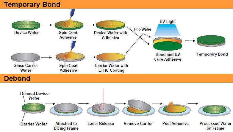
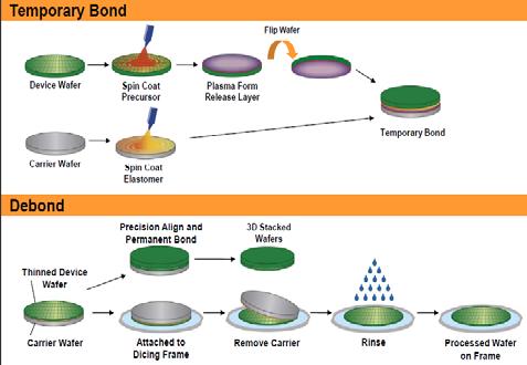

14 Thin Wafer Handling - Temporally Bonding/Debonding BSI Thermal plastic adhesive TMAT Mechanically released adhesive 3M Laser released adhesive TOK Chemical released adhesive
 Stand off Low Temperature Solder (180 C) Cu pillar with leadfree solder (260 C) Specification On going Research: C2W bonding : 10 chips")
15 Chip Stacking Process Key challenges: Multiple chip stacking with low stand off interconnection Low warpage wafer level encapsulation Wafer Level Underfilling Base Wafer Chuck C2C & C2W Bonding Base Wafer Wafer Level Molding Description Bonding method (C2W, C2C) Stand off Low Temperature Solder (180 C) Cu pillar with leadfree solder (260 C) Specification On going Research: C2W bonding : 10 chips Interconnection: RDLless and Bumpless Micro joint Thermo compression 5um 15um
16 Reliability Challenges Stress concentration, Cracks around TSVs IMC, fatigue failure of microbumps Moisture induced delamination, corrosion Substrate Hot Spot in Chip & Thermal Management Electromigration in Microbumps & TSVs
17 Sensor Chip Design For Reliability R 1 ' y [ 1 00] y[ 1 10] ' x [ 010] x[ 110] R 4 R 3 R 2 Stress sensor for process development Comb & Triple Tracks Sensor for moisture ingress & corrosion N++ P + implant N++ P + implant n-well n-well p substrate Thermal chip design Crack sensor chip design

 Micro Channels Seal ring Fluidic Inlet TSV Electrical I/O Integrated single or two phase liquid cooling for high power chips in 3DIC Chip carrier with")
18 Integrated Cooling Solution Heat Exchanger Mini Pump Fluidic adaptor Silicon carrier PCB Avg. Chip Temperature ( C) Chip with 400 Bumps ( Measured Data) Chip with 2500 Bumps ( Simulation Data) Avg Cooling Liquid Temp Chip Heat Dissipation (W/cm2) Micro Channels Seal ring Fluidic Inlet TSV Electrical I/O Integrated single or two phase liquid cooling for high power chips in 3DIC Chip carrier with fluidic and electrical paths by C2C bonding 3D electrical and fluidic interconnection using silicon interposer On going Research: Two Phase Boiling Cooling
19 Singapore 3D TSV Consortium 1 st Year Phase 1 (18 months) 2 nd Year 3 rd Year Phase 2 (18 months) Design & Modeling Studies Process & Reliability studies Identify & establishment 300mm line through consortium efforts Process & Characterization studies on 300mm wafer Application: Mobile Devices One Logic Chip & Six Memory Chips Consortium Deliverables: Phase 1: Design Guidelines & Process Development Phase 2: Full Functional Device Demonstration


20 IME 3DIC Development Roadmap Design, Simulation & Characterization Sensor + Mixed Signal Sensor + Memory + FPGA PMIC + Memory + RFIC TSV Fabrication Thermo-Mechanical simulation Dynamic two-phase flow simulation High freq. (up to 80GHz) TSV Electrical Characterization (Φ<2um, D<20um) Sub-micron Via Φ1um, D10um Via Last Φ5um, D50um Via Middle Φ2um, D20um Wafer Handling & Thinning 12 20um thickness 12 10um thickness 8 50um thickness 12 50um thickness Wafer Level RDL & Micro-bumping Line/Space: 15um/15um Line/Space: 10um/10um CuInSn solder: 180 C, Size: 8um, Pitch: 15um 3D Stacking (C2C, C2W, W2W) W2W Cu-Cu Bonding (Pad size: 5um, pitch: 10um, Bonding temp.: <200 C) C2C/C2W bonding with solder (10 chips)
21 3DIC Product Development Challenges Infrastructure availability and supply chain I/O standardization between interfaces Thermal management and interconnect reliability Shift in the Design/Test method paradigm and system co design
22 Thank you for your attention!
Thin Wafers Bonding & Processing
 Thin Wafers Bonding & Processing A market perspective 2012 Why New Handling Technologies Consumer electronics is today a big driver for smaller, higher performing & lower cost device configurations. These
TSV Interposer Process Flow with IME 300mm Facilities
 TSV Interposer Process Flow with IME 300mm Facilities Property of Institute of Microelectronics (IME)-Singapore August 17, 2012 Outline 1. TSV interposer (TSI) cross sectional schematic TSI with BEOL,
Cu Pillar Interconnect and Chip-Package-Interaction (CPI) for Advanced Cu Low K chip
 for Advanced Cu Low K chip") EPRC 12 Project Proposal Cu Pillar Interconnect and Chip-Package-Interaction (CPI) for Advanced Cu Low K chip 15 th Aug 2012 Page 1 Introduction: Motivation / Challenge Silicon device with ultra low k
EPRC 12 Project Proposal Cu Pillar Interconnect and Chip-Package-Interaction (CPI) for Advanced Cu Low K chip 15 th Aug 2012 Page 1 Introduction: Motivation / Challenge Silicon device with ultra low k
Hot Chips: Stacking Tutorial
 Hot Chips: Stacking Tutorial Choon Lee Technology HQ, Amkor Enabling a Microelectronic World Mobile Phone Technology Change Feature Phone Smartphone Smartphones as a Percentage of All Phones Source : The
IME Technical Proposal. High Density FOWLP for Mobile Applications. 22 April High Density FOWLP Consortium Forum
 IME Technical Proposal High Density FOWLP for Mobile Applications 22 April 2014 Packaging driver for portable / mobile applications Key drivers/needs Smaller form-factor lower profile, substrate-less Higher
TGV and Integrated Electronics
 TGV and Integrated Electronics Shin Takahashi ASAHI GLASS CO., LTD. 1 Ambient Intelligence Green Energy/Environment Smart Factory Smart Mobility Smart Mobile Devices Bio/Medical Security/Biometrics 2 Glass
Challenges and Solutions for Cost Effective Next Generation Advanced Packaging. H.P. Wirtz, Ph.D. MiNaPAD Conference, Grenoble April 2012
 Challenges and Solutions for Cost Effective Next Generation Advanced Packaging H.P. Wirtz, Ph.D. MiNaPAD Conference, Grenoble April 2012 Outline Next Generation Package Requirements ewlb (Fan-Out Wafer
3D technologies for integration of MEMS
 3D technologies for integration of MEMS, Fraunhofer Institute for Electronic Nano Systems Folie 1 Outlook Introduction 3D Processes Process integration Characterization Sample Applications Conclusion Folie
TSV Processing and Wafer Stacking. Kathy Cook and Maggie Zoberbier, 3D Business Development
 TSV Processing and Wafer Stacking Kathy Cook and Maggie Zoberbier, 3D Business Development Outline Why 3D Integration? TSV Process Variations Lithography Process Results Stacking Technology Wafer Bonding
An Innovative High Throughput Thermal Compression Bonding Process
 An Innovative High Throughput Thermal Compression Bonding Process Li Ming 2 September 2015 Outline Introduction Throughput improved TCB Process Liquid Phase Contact (LPC) bonding Flux-LPC-TCB under inert
Novel Materials and Activities for Next Generation Package. Hitachi Chemical., Co.Ltd. Packaging Solution Center Hiroaki Miyajima
 Novel Materials and Activities for Next Generation Package Hitachi Chemical., Co.Ltd. Packaging Solution Center Hiroaki Miyajima 1. Activities of Packaging Solution Center 2. Novel Materials for Next Gen.
Panel Discussion: Advanced Packaging
 Dr. Steve Bezuk Senior Director IC Packaging Engineering Qualcomm Technologies, Inc. Panel Discussion: Advanced Packaging PAGE 1 Technical Challenges of Packaging (Mobile Focus) Materials Die materials
3D Package Technologies Review with Gap Analysis for Mobile Application Requirements. Apr 22, 2014 STATS ChipPAC Japan
 3D Package Technologies Review with Gap Analysis for Mobile Application Requirements Apr 22, 2014 STATS ChipPAC Japan T.Nishio Contents Package trends and roadmap update Advanced technology update Fine
Embedded Cooling Solutions for 3D Packaging
 IME roprietary ERC 12 roject roposal Embedded Cooling Solutions for 3D ackaging 15 th August 2012 age 1 Technology & ower Dissipation Trends IME roprietary Cannot continue based on Moore s law scaling
Thermo-Mechanical Reliability of Through-Silicon Vias (TSVs)
") 1 Thermo-Mechanical Reliability of Through-Silicon Vias (TSVs) Xi Liu Ph.D. Student and Suresh K. Sitaraman, Ph.D. Professor The George W. Woodruff School of Mechanical Engineering Georgia Institute of
1 Thermo-Mechanical Reliability of Through-Silicon Vias (TSVs) Xi Liu Ph.D. Student and Suresh K. Sitaraman, Ph.D. Professor The George W. Woodruff School of Mechanical Engineering Georgia Institute of
Copyright 2009 Year IEEE. Reprinted from 2009 Electronic Components and Technology Conference. Such permission of the IEEE does not in any way imply
 Copyright 2009 Year IEEE. Reprinted from 2009 Electronic Components and Technology Conference. Such permission of the IEEE does not in any way imply IEEE endorsement of any of Institute of Microelectronics
Chips Face-up Panelization Approach For Fan-out Packaging
 Chips Face-up Panelization Approach For Fan-out Packaging Oct. 15, 2015 B. Rogers, D. Sanchez, C. Bishop, C. Sandstrom, C. Scanlan, TOlson T. REV A Background on FOWLP Fan-Out Wafer Level Packaging o Chips
3D technologies for More Efficient Product Development
 3D technologies for More Efficient Product Development H. Ribot, D. Bloch, S. Cheramy, Y. Lamy, P. Leduc, T. Signamarcheix, G. Simon Semicon Europa, TechArena II, 09 October 2013 Photonics in Product development:
Power Electronics Packaging Solutions for Device Junction Temperature over 220 o C
 EPRC 12 Project Proposal Power Electronics Packaging Solutions for Device Junction Temperature over 220 o C 15 th August 2012 Page 1 Motivation Increased requirements of high power semiconductor device
CMP Process Development for the Via- Middle 3D TSV Applications at 28nm Technology Node
 CMP Process Development for the Via- Middle 3D TSV Applications at 28nm Technology Node UMC/ ATD_AM / CMP Department T. C. Tsai, W. C. Tsao, Welch Lin, C. L. Hsu, C. L. Lin, C. M. Hsu, J. F. Lin, C. C.
Innovative Substrate Technologies in the Era of IoTs
 Innovative Substrate Technologies in the Era of IoTs Dyi- Chung Hu 胡迪群 September 4, 2015 Unimicron Contents Introduction Substrate Technology - Evolution Substrate Technology - Revolution Glass substrate
FABRICATION AND RELIABILITY OF ULTRA-FINE RDL STRUCTURES IN ADVANCED PACKAGING BY EXCIMER LASER ABLATION
 FABRICATION AND RELIABILITY OF ULTRA-FINE RDL STRUCTURES IN ADVANCED PACKAGING BY EXCIMER LASER ABLATION NCCAVS Joint Users Group Technical Symposium San Jose, June 7 th, 2017 Markus Arendt, SÜSS MicroTec
Packaging Effect on Reliability for Cu/Low k Damascene Structures*
 Packaging Effect on Reliability for Cu/Low k Damascene Structures* Guotao Wang and Paul S. Ho Laboratory of Interconnect & Packaging, TX 78712 * Work supported by SRC through the CAIST Program TRC 2003
FOR SEMICONDUCTORS 2007 EDITION
 INTERNATIONAL TECHNOLOGY ROADMAP FOR SEMICONDUCTORS 2007 EDITION ASSEMBLY AND PACKAGING THE ITRS IS DEVISED AND INTENDED FOR TECHNOLOGY ASSESSMENT ONLY AND IS WITHOUT REGARD TO ANY COMMERCIAL CONSIDERATIONS
IME Proprietary. EPRC 12 Project Proposal. 3D Embedded WLP. 15 th August 2012
 EPRC 12 Project Proposal 3D Embedded WLP 15 th August 2012 Motivation Factors driving IC market Higher density, lower cost, high yield Fan-out WLP/eWLP advantages Small footprint, low profile Low cost,
FRAUNHOFER INSTITUTE FOR RELIABILITY AND MICROINTEGRATION IZM DEPARTMENT WAFER LEVEL SYSTEM INTEGRATION BERLIN
 FRAUNHOFER INSTITUTE FOR RELIABILITY AND MICROINTEGRATION IZM DEPARTMENT WAFER LEVEL SYSTEM INTEGRATION BERLIN WAFER LEVEL SYSTEM INTEGRATION ELECTRONIC PACKAGING AT FRAUNHOFER IZM The Fraunhofer Institute
Evaluation of Cu Pillar Chemistries
 Presented at 2016 IMAPS Device Packaging Evaluation of Cu Pillar Chemistries imaps Device Packaging Conference Spring 2016 Matthew Thorseth, Mark Scalisi, Inho Lee, Sang-Min Park, Yil-Hak Lee, Jonathan
/15/$ IEEE Electronic Components & Technology Conference
 Demonstration of 2µm RDL Wiring Using Dry Film Photoresists and 5µm RDL Via by Projection Lithography for Low-cost 2.5D Panel-based Glass and Organic Interposers Ryuta Furuya*, Hao Lu**, Fuhan Liu**, Hai
Ultra Fine Pitch Bumping Using e-ni/au and Sn Lift-Off Processes
 Ultra Fine Pitch Bumping Using e-ni/au and Sn Lift-Off Processes Andrew Strandjord, Thorsten Teutsch, and Jing Li Pac Tech USA Packaging Technologies, Inc. Santa Clara, CA USA 95050 Thomas Oppert, and
Chapter 3 Silicon Device Fabrication Technology
 Chapter 3 Silicon Device Fabrication Technology Over 10 15 transistors (or 100,000 for every person in the world) are manufactured every year. VLSI (Very Large Scale Integration) ULSI (Ultra Large Scale
2.5D and 3D Semiconductor Package Technology: Evolution and Innovation
 2.5D and 3D Semiconductor Package Technology: Evolution and Innovation Vern Solberg Solberg Technical Consulting Saratoga, California USA Abstract The electronics industry is experiencing a renaissance
SEMI Networking Day 2013 Rudolph Corporate Introduction
 SEMI Networking Day 2013 Rudolph Corporate Introduction Rudolph Technologies: Corporate Profile Business: Semiconductor capital equipment company dedicated exclusively to inspection, advanced packaging
Roundtable 3DIC & TSV: Ready for HVM? European 3D TSV Summit
 Roundtable 3DIC & TSV: Ready for HVM? European 3D TSV Summit Infineon VTI Xilinx Synopsys Micron CEA LETI 2013 Yann Guillou Business Development Manager Lionel Cadix Market & Technology Analyst, Advanced
200mm Next Generation MEMS Technology update. Florent Ducrot
 200mm Next Generation MEMS Technology update Florent Ducrot The Most Exciting Industries on Earth Semiconductor Display Solar 20,000,000x reduction in COST PER TRANSISTOR in 30 years 1 20x reduction in
TSV and Cu-Cu Direct Bond Wafer and Package-Level Reliability
 TSV and Cu-Cu Direct Bond Wafer and Package-Level Reliability K. Hummler 1, B. Sapp 1, J.R. Lloyd 2, S. Kruger 1, 2 S. Olson 1, 2, SB Park 3, B. Murray 3, D. Jung 3, S. Cain 3, A. Park 3, D. Ferrone 3,
TSV Formation: Drilling and Filling
 3D Architectures for Semiconductor Integration and Packaging (3D ASIP), Burlingame, CA, Dec. 10-12, 2014 Preconference symposium- 3D Integration: 3D Process Technology TSV Formation: Drilling and Filling
Overview of CMP for TSV Applications. Robert L. Rhoades, Ph.D. Presentation for AVS Joint Meeting June 2013 San Jose, CA
 Overview of CMP for TSV Applications Robert L. Rhoades, Ph.D. Presentation for AVS Joint Meeting June 2013 San Jose, CA Outline TSV s and the Role of CMP TSV Pattern and Fill TSV Reveal (non-selective)
II. A. Basic Concept of Package.
 Wafer Level Package for Image Sensor Module Won Kyu Jeung, Chang Hyun Lim, Jingli Yuan, Seung Wook Park Samsung Electro-Mechanics Co., LTD 314, Maetan3-Dong, Yeongtong-Gu, Suwon, Gyunggi-Do, Korea 440-743
Close supply chain collaboration enables easy implementation of chip embedded power SiP
 Close supply chain collaboration enables easy implementation of chip embedded power SiP Gerald Weidinger, R&D Project Leader, AT&S AT & S Austria Technologie & Systemtechnik Aktiengesellschaft Fabriksgasse13
Silicon Interposer with Embedded Microfluidic Cooling for High-Performance Computing Systems
 Silicon Interposer with Embedded Microfluidic Cooling for High-Performance Computing Systems Li Zheng 1, Yang Zhang, Xuchen Zhang and Muhannad S. Bakir 2 School of Electrical and Computer Engineering Georgia
Cost effective 300mm Large Scale ewlb (embedded Wafer Level BGA) Technology
 Technology") Cost effective 300mm Large Scale ewlb (embedded Wafer Level BGA) Technology by Meenakshi Prashant, Seung Wook Yoon, Yaojian LIN and Pandi C. Marimuthu STATS ChipPAC Ltd. 5 Yishun Street 23, Singapore 768442
Cost effective 300mm Large Scale ewlb (embedded Wafer Level BGA) Technology by Meenakshi Prashant, Seung Wook Yoon, Yaojian LIN and Pandi C. Marimuthu STATS ChipPAC Ltd. 5 Yishun Street 23, Singapore 768442
Avatrel Stress Buffer Coatings: Low Stress Passivation and Redistribution Applications
 Avatrel Stress Buffer Coatings: Low Stress Passivation and Redistribution Applications Ed Elce, Chris Apanius, Jeff Krotine, Jim Sperk, Andrew Bell, Rob Shick* Sue Bidstrup-Allen, Paul Kohl Takashi Hirano,
RF System in Packages using Integrated Passive Devices
 RF System in Packages using Integrated Passive Devices by Kai Liu, YongTaek Lee, HyunTai Kim, Gwang Kim, and Billy Ahn STATS ChipPAC 1711 W. Greentree Drive, Suite #117, Tempe, AZ 85284, USA Tel: 480-222-1722
TSV CHIP STACKING MEETS PRODUCTIVITY
 TSV CHIP STACKING MEETS PRODUCTIVITY EUROPEAN 3D TSV SUMMIT 22-23.1.2013 GRENOBLE HANNES KOSTNER DIRECTOR R&D BESI AUSTRIA OVERVIEW Flip Chip Packaging Evolution The Simple World of C4 New Flip Chip Demands
3D & 2½D Test Challenges Getting to Known Good Die & Known Good Stack
 1 3D & 2½D Test Challenges Getting to Known Good Die & Known Good Stack Advantest Corporation 2 The final yield Any Multi-die Product Must Consider the Accumulated Yield Assume Test Can Provide 99% Die
Glass Carrier for Fan Out Panel Level Package
 January 25, 2018 NEWS RELEASE Development of HRDP TM Material for Formation of Ultra-Fine Circuits with Glass Carrier for Fan Out Panel Level Package - Aiming for mass production in collaboration with
3D-IC Fabrication Challenges for More Than Moore Applications
 3D-IC Fabrication Challenges for More Than Moore Applications Armin Klumpp and Peter Ramm Fraunhofer IZM, Munich Hansastrasse 27d, 80686 Munich, Germany peter.ramm@izm-m.fraunhofer.de Definition: 3D Integration
Recent Advances in Die Attach Film
 Recent Advances in Die Attach Film Frederick Lo, Maurice Leblon, Richard Amigh, and Kevin Chung. AI Technology, Inc. 70 Washington Road, Princeton Junction, NJ 08550 www.aitechnology.com Abstract: The
IMPLEMENTATION OF A FULLY MOLDED FAN-OUT PACKAGING TECHNOLOGY
 IMPLEMENTATION OF A FULLY MOLDED FAN-OUT PACKAGING TECHNOLOGY B. Rogers, C. Scanlan, and T. Olson Deca Technologies, Inc. Tempe, AZ USA boyd.rogers@decatechnologies.com ABSTRACT Fan-Out Wafer-Level Packaging
Images of Failures in Microelectronics Packaging and Assembly
 Images of Failures in Microelectronics Packaging and Assembly Ed Hare, Ph.D./SEM Lab, Inc. IMAPS NW - Feb. 11th 2004 Redmond, WA http://www.semlab.com 1 What is this? http://www.semlab.com 2 Inner Layer
Copyright 2008 Year IEEE. Reprinted from IEEE TRANSACTIONS ON ADVANCED PACKAGING, VOL. 31, NO. 1, FEBRUARY Such permission of the IEEE does not
 Copyright 2008 Year IEEE. Reprinted from IEEE TRANSACTIONS ON ADVANCED PACKAGING, VOL. 31, NO. 1, FEBRUARY 2008. Such permission of the IEEE does not in any way imply IEEE endorsement of any of Institute
Ultralow Residue Semiconductor Grade Fluxes for Copper Pillar Flip-Chip
 Ultralow Residue Semiconductor Grade Fluxes for Copper Pillar Flip-Chip SzePei Lim (Presenter), Jason Chou, Maria Durham, and Dr. Andy Mackie Indium Corporation 1 Outline of Presentation Roadmaps and challenges
New Technology for High-Density LSI Mounting in Consumer Products
 New Technology for High-Density Mounting in Consumer Products V Hidehiko Kira V Akira Takashima V Yukio Ozaki (Manuscript received May 29, 2006) The ongoing trend toward downsizing and the growing sophistication
Atul Gupta, Eric Snyder, Christiane Gottschalk, Kevin Wenzel, James Gunn
 First Demonstration of Photoresist Cleaning for Fine-Line RDL Yield Enhancement by an Innovative Ozone Treatment Process for Panel Fan-out and Interposers Atul Gupta, Eric Snyder, Christiane Gottschalk,
Fanout Flipchip ewlb (embedded Wafer Level Ball Grid Array) Technology as 2.5D Packaging Solution
 Technology as 2.5D Packaging Solution") Fanout Flipchip ewlb (embedded Wafer Level Ball Grid Array) Technology as 2.5D Packaging Solution by Seung Wook Yoon,*Patrick Tang, **Roger Emigh, Yaojian Lin, Pandi C. Marimuthu, and *Raj Pendse STATS
Fanout Flipchip ewlb (embedded Wafer Level Ball Grid Array) Technology as 2.5D Packaging Solution by Seung Wook Yoon,*Patrick Tang, **Roger Emigh, Yaojian Lin, Pandi C. Marimuthu, and *Raj Pendse STATS
SEMI MEMS Tech Seminar (Sept 26, Cornaredo, Italy)
") SEMI MEMS Tech Seminar (Sept 26, 2013 - Cornaredo, Italy) Opportunities of Wafer Level Embedded Technologies for MEMS Devices T. Braun ( 1 ), K.-F. Becker ( 1 ), R. Kahle ( 2 ), V. Bader ( 1 ), S. Voges
SEMI MEMS Tech Seminar (Sept 26, 2013 - Cornaredo, Italy) Opportunities of Wafer Level Embedded Technologies for MEMS Devices T. Braun ( 1 ), K.-F. Becker ( 1 ), R. Kahle ( 2 ), V. Bader ( 1 ), S. Voges
EECS130 Integrated Circuit Devices
 EECS130 Integrated Circuit Devices Professor Ali Javey 9/13/2007 Fabrication Technology Lecture 1 Silicon Device Fabrication Technology Over 10 15 transistors (or 100,000 for every person in the world)
Two Chips Vertical Direction Embedded Miniaturized Package
 Two Chips Vertical Direction Embedded Miniaturized Package Shunsuke Sato, 1 Koji Munakata, 1 Masakazu Sato, 1 Atsushi Itabashi, 1 and Masatoshi Inaba 1 Continuous efforts have been made to achieve seemingly
1 Thin-film applications to microelectronic technology
 1 Thin-film applications to microelectronic technology 1.1 Introduction Layered thin-film structures are used in microelectronic, opto-electronic, flat panel display, and electronic packaging technologies.
Thermo-Mechanical Reliability Assessment of TSV Die Stacks by Finite Element Analysis
 Thermo-Mechanical Reliability Assessment of TSV Die Stacks by Finite Element Analysis Dr. Roland Irsigler, emens AG Corporate Technology, CT T P HTC Outline TSV SOLID µbump Stacking TSV application FEA
Outline. Market Size Industry Trends Material Segment Trends China Summary. Packaging Materials Market Trends, Issues and Opportunities
 Packaging Materials Market Trends, Issues and Opportunities Dan Tracy Sr. Director Industry Research SEMI 8 th December 2015 Outline Market Size Industry Trends Material Segment Trends China Summary 1
"ewlb Technology: Advanced Semiconductor Packaging Solutions"
 "ewlb Technology: Advanced Semiconductor Packaging Solutions" by Sharma Gaurav@, S.W. Yoon, Yap Yok Mian, Shanmugam Karthik, Yaojian Lin, Pandi C. Marimuthu and Yeong J. Lee* STATS ChipPAC Ltd. 5 Yishun
Micro-Electro-Mechanical Systems (MEMS) Fabrication. Special Process Modules for MEMS. Principle of Sensing and Actuation
 Fabrication. Special Process Modules for MEMS. Principle of Sensing and Actuation") Micro-Electro-Mechanical Systems (MEMS) Fabrication Fabrication Considerations Stress-Strain, Thin-film Stress, Stiction Special Process Modules for MEMS Bonding, Cavity Sealing, Deep RIE, Spatial forming
Micro-Electro-Mechanical Systems (MEMS) Fabrication Fabrication Considerations Stress-Strain, Thin-film Stress, Stiction Special Process Modules for MEMS Bonding, Cavity Sealing, Deep RIE, Spatial forming
The ABC s of CMP for DWB and SOI. Robert L. Rhoades, Ph.D. CAMP Conference Presentation August 9, 2010
 The ABC s of CMP for DWB and SOI Robert L. Rhoades, Ph.D. CAMP Conference Presentation August 9, 2010 Outline Introduction Direct Wafer Bonding (DWB) Background CMP for DWB Silicon-On-Insulator (SOI) Background
Semiconductor IC Packaging Technology Challenges: The Next Five Years
 SPAY025 May 2006 White Paper Mario A. Bolanos, Director Semiconductor Group Packaging Technology Development, Texas Instruments In the era of communications and entertainment, growth of consumer electronics
Enabling Materials Technology for Multi-Die Integration
 Enabling Materials Technology for Multi-Die Integration Dr. Jeffrey M. Calvert Global R&D Director, Advanced Packaging Technologies Dow Electronic Materials 455 Forest St., Marlborough, MA 01752 USA jcalvert@dow.com
3D Integrated ewlb /FO-WLP Technology for PoP & SiP
 3D Integrated ewlb /FO-WLP Technology for PoP & SiP by Yaojian Lin, Chen Kang, Linda Chua, Won Kyung Choi and *Seung Wook Yoon STATS ChipPAC Pte Ltd. 5 Yishun Street 23, Singapore 768442 *STATS ChipPAC
Plasma for Underfill Process in Flip Chip Packaging
 Plasma for Underfill Process in Flip Chip Packaging Jack Zhao and James D. Getty Nordson MARCH 2470-A Bates Avenue Concord, California 94520-1294 USA Published by Nordson MARCH www.nordsonmarch.com 2015
Automotive Electronic Material Challenges. Anitha Sinkfield, Delphi
 Automotive Electronic Material Challenges Anitha Sinkfield, Delphi Automotive Electronic Material Challenges Project Update About inemi Project Participants Problem Statement Project Details Summary and
Copyright 2008 Year IEEE. Reprinted from IEEE ECTC May 2008, Florida USA.. This material is posted here with permission of the IEEE.
 Copyright 2008 Year IEEE. Reprinted from IEEE ECTC 2008. 27-30 May 2008, Florida USA.. This material is posted here with permission of the IEEE. Such permission of the IEEE does not in any way imply IEEE
Materials Characterization for Stress Management
 Materials Characterization for Stress Management Ehrenfried Zschech, Fraunhofer IZFP Dresden, Germany Workshop on Stress Management for 3D ICs using TSVs San Francisco/CA, July 13, 2010 Outline Stress
Copper Wire Packaging Reliability for Automotive and High Voltage
 Copper Wire Packaging Reliability for Automotive and High Voltage Tu Anh Tran AMPG Package Technology Manager Aug.11.2015 TM External Use Agenda New Automotive Environments Wire Bond Interconnect Selection
Reliability Challenges for 3D Interconnects:
 Reliability Challenges for 3D Interconnects: A material and design perspective Paul S. Ho Suk-Kyu Ryu, Kuan H. (Gary) Lu, Qiu Zhao, Jay Im and Rui Huang The University of Texas at Austin 3D Sematech Workshop,
Challenges for Embedded Device Technologies for Package Level Integration
 Challenges for Embedded Device Technologies for Package Level Integration Kevin Cannon, Steve Riches Tribus-D Ltd Guangbin Dou, Andrew Holmes Imperial College London Embedded Die Technology IMAPS-UK/NMI
3D Wirebondless IGBT Module for High Power Applications Dr. Ziyang GAO Jun. 20, 2014
 3D Wirebondless IGBT Module for High Power Applications Dr. Ziyang GAO Jun. 20, 2014 1 1 Outline Background Information Technology Development Trend Technical Challenges ASTRI s Solutions Concluding Remarks
Wire-Bond CABGA A New Near Die Size Packaging Innovation Yeonho Choi February 1, 2017
 Amkor Technology, Inc. White Paper Wire-Bond CABGA A New Near Die Size Packaging Innovation Yeonho Choi February 1, 2017 Abstract Expanding its ChipArray Ball Grid Array (CABGA) package form factor miniaturization
Interconnects. Outline. Interconnect scaling issues Aluminum technology Copper technology. Properties of Interconnect Materials
 Interconnects Outline Interconnect scaling issues Aluminum technology Copper technology 1 Properties of Interconnect Materials Metals Silicides Barriers Material Thin film Melting resistivity point ( C)
23 rd ASEMEP National Technical Symposium
 THE EFFECT OF GLUE BOND LINE THICKNESS (BLT) AND FILLET HEIGHT ON INTERFACE DELAMINATION Raymund Y. Agustin Janet M. Jucar Jefferson S. Talledo Corporate Packaging & Automation/ Q&R STMicroelectronics,
Test Flow for Advanced Packages (2.5D/SLIM/3D)
") 1 Test Flow for Advanced Packages (2.5D/SLIM/3D) Gerard John Amkor Technology Inc. Gerard.John@amkor.com 2045 East Innovation Circle, Tempe, AZ 85284, USA Phone: (480) 821-5000 ADVANCED PACKAGE TEST FLOW
1 Test Flow for Advanced Packages (2.5D/SLIM/3D) Gerard John Amkor Technology Inc. Gerard.John@amkor.com 2045 East Innovation Circle, Tempe, AZ 85284, USA Phone: (480) 821-5000 ADVANCED PACKAGE TEST FLOW
3D Packaging- Synthetic Quartz Substrate and Interposers for High Frequency Applications. Vern Stygar #1, Tim Mobley* 2 # Asahi Glass Corporation
 3D Packaging- Synthetic Quartz Substrate and Interposers for High Frequency Applications Vern Stygar #1, Tim Mobley* 2 # Asahi Glass Corporation 4375 Northwest 235 th Avenue, Hillsboro OR USA 97124 1 vstygar@agem.com
Forecast of Used Equipment Market Based on Demand & Supply
 Forecast of Used Equipment Market Based on Demand & Supply 2013. 06. 05 Thomas LEE Ⅰ. Market Introduction 300 200 150 _ Wafer Demand by Devices Type and Used Equipment Targets 20 to 0.13 0.13 to 0.5 >
TechARENA Packaging Exhibitor Session OCT/08, 2014 New WLP-Technology-Fusion Concept Steffen Kröhnert, Director of Technology, NANIUM S.A. V1.
 TechARENA Packaging Exhibitor Session OCT/08, 2014 New WLP-Technology-Fusion Concept Steffen Kröhnert, Director of Technology, NANIUM S.A. V1.0 EXT Notification NANIUM is highly committed to IP protection.
Silicon Interposers with Integrated Passive Devices: Ultra-Miniaturized Solution using 2.5D Packaging Platform
 Minapad 2014, May 21 22th, Grenoble; France Silicon Interposers with Integrated Passive Devices: Ultra-Miniaturized Solution using 2.5D Packaging Platform Stéphane Bellenger, Laëtitia Omnès, Jean-René
3D-WLCSP Package Technology: Processing and Reliability Characterization
 3D-WLCSP Package Technology: Processing and Reliability Characterization, Paul N. Houston, Brian Lewis, Fei Xie, Ph.D., Zhaozhi Li, Ph.D.* ENGENT Inc. * Auburn University ENGENT, Inc. 2012 1 Outline Packaging
Hitachi A 64Mbit (8Mb x 8) Dynamic RAM
 Dynamic RAM") Construction Analysis Hitachi 5165805A 64Mbit (8Mb x 8) Dynamic RAM Report Number: SCA 9712-565 Global Semiconductor Industry the Serving Since 1964 17350 N. Hartford Drive Scottsdale, AZ 85255 Phone:
Construction Analysis Hitachi 5165805A 64Mbit (8Mb x 8) Dynamic RAM Report Number: SCA 9712-565 Global Semiconductor Industry the Serving Since 1964 17350 N. Hartford Drive Scottsdale, AZ 85255 Phone:
Challenges and Future Directions of Laser Fuse Processing in Memory Repair
 Challenges and Future Directions of Laser Fuse Processing in Memory Repair Bo Gu, * T. Coughlin, B. Maxwell, J. Griffiths, J. Lee, J. Cordingley, S. Johnson, E. Karagiannis, J. Ehrmann GSI Lumonics, Inc.
Advancements In Packaging Technology Driven By Global Market Return. M. G. Todd
 Advancements In Packaging Technology Driven By Global Market Return M. G. Todd Electronic Materials, Henkel Corporation, Irvine, California 92618, USA Recently, the focus of attention in the IC packaging
Through Silicon Vias Annealing: A thermo-mechanical assessment
 Dresden University of Technology / Through Silicon Vias Annealing: P. Saettler (1), K. J. Wolter (1), M. Hecker (2), M. Boettcher (3) and C. Rudolph (3) (1) Technische Universität Dresden, (2) Globalfoundries
Failure Modes in Wire bonded and Flip Chip Packages
 Failure Modes in Wire bonded and Flip Chip Packages Mumtaz Y. Bora Peregrine Semiconductor San Diego, Ca. 92121 mbora@psemi.com Abstract The growth of portable and wireless products is driving the miniaturization
Improvement of Laser Fuse Processing of Fine Pitch Link Structures for Advanced Memory Designs
 Improvement of Laser Fuse Processing of Fine Pitch Link Structures for Advanced Memory Designs Joohan Lee, Joseph J. Griffiths, and James Cordingley GSI Group Inc. 60 Fordham Rd. Wilmington, MA 01887 jlee@gsig.com
Nondestructive Internal Inspection. The World s Leading Acoustic Micro Imaging Lab
 Nondestructive Internal Inspection The World s Leading Acoustic Micro Imaging Lab Unmatched Capabilities and Extensive Expertise At Your Service SonoLab, a division of Sonoscan, is the world s largest
WF6317. A superactive low-volatile/high heat-resistant water-soluble flux for ball soldering
 WF637 A superactive low-volatile/high heat-resistant water-soluble flux for ball soldering Low viscosity and high tacking power stabilize ball holding force and ensures excellent solder wettability Easy
28nm Mobile SoC Copper Pillar Probing Study. Jose Horas (Intel Mobile Communications) Amy Leong (MicroProbe) Darko Hulic (Nikad)
 Amy Leong (MicroProbe) Darko Hulic (Nikad)") 28nm Mobile SoC Copper Pillar Probing Study Jose Horas (Intel Mobile Communications) Amy Leong (MicroProbe) Darko Hulic (Nikad) Overview Introduction to IMC Copper Pillar Implementation at IMC Low force
28nm Mobile SoC Copper Pillar Probing Study Jose Horas (Intel Mobile Communications) Amy Leong (MicroProbe) Darko Hulic (Nikad) Overview Introduction to IMC Copper Pillar Implementation at IMC Low force
Board Level Reliability Improvement in ewlb (Embedded Wafer Level BGA) Packages
 Packages") Board Level Reliability Improvement in ewlb (Embedded Wafer Level BGA) Packages by Seng Guan Chow, Yaojian Lin, Bernard Adams * and Seung Wook Yoon** STATS ChipPAC Ltd. 5 Yishun Street 23, Singapore 768442
Board Level Reliability Improvement in ewlb (Embedded Wafer Level BGA) Packages by Seng Guan Chow, Yaojian Lin, Bernard Adams * and Seung Wook Yoon** STATS ChipPAC Ltd. 5 Yishun Street 23, Singapore 768442
EE 330 Lecture 9. IC Fabrication Technology Part II. -Oxidation -Epitaxy -Polysilicon -Planarization -Resistance and Capacitance in Interconnects
 EE 330 Lecture 9 IC Fabrication Technology Part II -Oxidation -Epitaxy -Polysilicon -Planarization -Resistance and Capacitance in Interconnects Review from Last Time Etching Dry etch (anisotropic) SiO
Design for Flip-Chip and Chip-Size Package Technology
 Design for Flip-Chip and Chip-Size Package Technology Vern Solberg Solberg Technology Consulting Madison, Wisconsin Abstract As new generations of electronic products emerge they often surpass the capability
Design and Assembly Process Implementation of 3D Components
 IPC-7091 Design and Assembly Process Implementation of 3D Components Developed by the 3-D Electronic Packages Subcommittee (B-11) of the Packaged Electronic Components Committee (B-10) of IPC Users of
Lead-Free Solder Bump Technologies for Flip-Chip Packaging Applications
 Lead-Free Solder Bump Technologies for Flip-Chip Packaging Applications Zaheed S. Karim 1 and Jim Martin 2 1 Advanced Interconnect Technology Ltd. 1901 Sunley Centre, 9 Wing Yin Street, Tsuen Wan, Hong
Semiconductor Manufacturing Technology. IC Fabrication Process Overview
 Semiconductor Manufacturing Technology Michael Quirk & Julian Serda October 00 by Prentice Hall Chapter 9 IC Fabrication Process Overview /4 Objectives After studying the material in this chapter, you