VLSI PROCESS TECHNOLOGY By ER. HIMANSHU SHARMA
|
|
|
- Roxanne Thomas
- 5 years ago
- Views:
Transcription

1 VLSI PROCESS TECHNOLOGY y ER. HIMNSHU SHRM
2 Fabrication Masks Chips Wafers Processing Processed Wafer

3 Traditional CMOS Process
4 Modern CMOS Process Dual-Well Trench-Isolated CMOS gate oxide field oxide l (Cu) TiSi 2 SiO 2 tungsten n+ p well p-epi p- n well p+ SiO 2 Epi-layer is a high quality crystal grown on the polished surface of pre-doped silicon wafers for making CMOS nano devices.


.")
5 Photo-Lithographic Process oxidation optical mask photoresist removal (ashing) photoresist coating stepper exposure process step Typical operations in a single photolithographic cycle (from [Fullman]). spin, rinse, dry acid etch photoresist development

6 Growing the Silicon Ingot From Smithsonian, 2000

7 E-eam Lithography s the miniaturization of IC devices continues, electron beam exposure technology is gaining prominence as a technology for nextgeneration design rules From: DVNTEST CORPORTION

8 Silicon Oxidation The oxide is grown by exposing the silicon surface to high temperature steam. s the oxide grows, the silicon is consumed. The arrows represent the direction of motion of each surface of the oxide. Underneath the nitride mask, the growth is suppressed, and these areas will become the active transistor area. Source: ell Laboratories
9 Patterning - Photolithography 1. Oxidation 2. Photoresist (PR) coating 3. Stepper exposure SiO 2 4. Photoresist development and bake 5. cid etching Unexposed (negative PR) Exposed (positive PR) 6. Spin, rinse, and dry 7. Processing step Ion implantation Plasma etching Metal deposition 8. Photoresist removal (ashing) mask UV light PR
10 CMOS Process at a Glance Define active areas Etch and fill trenches Implant well regions Deposit and pattern polysilicon layer Implant source and drain regions and substrate contacts Create contact and via windows Deposit and pattern metal layers One full photolithography sequence per layer (mask) uilt (roughly) from the bottom up 5 metal 2 4 metal 1 2 polysilicon 3 source and drain diffusions 1 tubs (aka wells, active areas) exception!
11 Example of Patterning of SiO2 Si-substrate Silicon base material Si-substrate 1&2. fter oxidation and deposition of negative photoresist Si-substrate 3. Stepper exposure Photoresist SiO 2 UV-light Patterned optical mask Exposed resist Si-substrate Si-substrate 5. fter etching Si-substrate 8. Final result after removal of resist Chemical or plasma etch Hardened resist SiO 2 4. fter development and etching of resist, chemical or plasma etch of SiO 2 Hardened resist SiO 2 SiO 2
12 Diffusion and Ion Implantation 1. rea to be doped is exposed (photolithography) 2. Diffusion or Ion implantation

13 Ion Implantation 1. Dopant atoms are ionized and then accelerated by an electric field until they impinge on the silicon surface, where they embed themselves. 2. polysilicon line crosses the active area in the upper left and forms the gate of a transistor. Source: ell Laboratories
14 Deposition and Etching 1. Pattern masking (photolithography) 2. Deposit material over entire wafer CVD (Si 3 N 4 ) chemical deposition (polysilicon) sputtering (l) 3. Etch away unwanted material wet etching dry (plasma) etching

15 Metallization 1. First an insulating glass layer is deposited to cover the silicon, then contact holes are cut into the glass layer down to the silicon. 2. Metal is deposited on top of the glass, connecting to the devices through the contact holes. 3. The graphic shows a snapshot during the filling of a contact hole with aluminum. Source: ell Laboratories

16 F5112 E-eam Lithography Single-Column System Minimum Feature Size: 100nm Overlay ccuracy: mean +3 sigma<=40nm 3 sigma<=15nm lock Exposure Method: Max. No. of lock Patterns: 70

17 Planarization: Polishing the Wafers From Smithsonian, 2000
18 Self-ligned Gates 1. Create thin oxide in the active regions, thick elsewhere 2. Deposit polysilicon 3. Etch thin oxide from active region (poly acts as a mask for the diffusion) 4. Implant dopant
19 Simplified CMOS Inverter P-well Process cut line p well
20 P-Well Mask
21 ctive Mask
22 Poly Mask
23 P+ Select Mask
24 N+ Select Mask
25 Contact Mask
26 Metal Mask

27 VLSI Fabrication: The Cycle

28 CMOS N-well Process (cont d) The n-well CMOS process starts with a moderately doped (impurity concentration less than cm -3 ) p-type silicon substrate. Then, an oxide layer is grown on the entire surface. The first lithographic mask defines the n-well region. Donor atoms, usually phosphorus, are implanted through this window in the oxide. This defines, the active areas of the nmos and pmos transistors. Thin gate oxide is grown on top of the active regions. The thickness and the quality of the gate oxide are critical fabrication parameters, since they affect the characteristics of the MOS transistor, and its reliability.

29 CMOS N-well Process (cont d) The polysilicon layer is deposited using chemical vapor deposition (CVD) and patterned by dry (plasma) etching. The created polysilicon lines will function as the gate electrodes of the nmos and the pmos transistors and their interconnects. lso, the polysilicon gates act as self-aligned masks for the source and drain implantations that follow this step.

30 CMOS N-well Process (cont d) Using a set of two masks, the n+ and p+ regions are implanted into the substrate and into the n- well, respectively. The ohmic contacts to the substrate and to the n-well are implanted in this process step.

31 CMOS N-well Process (cont d) n insulating silicon dioxide layer is deposited over the entire wafer using CVD. Then, the contacts are defined and etched away to expose the silicon or polysilicon contact windows.

32 CMOS N-well Process (cont d) Metal is deposited over the entire chip surface using metal evaporation, and the metal lines are patterned through etching. Since the wafer surface is nonplanar, the quality and the integrity of the metal lines created in this step are very critical and are essential for circuit reliability.

33 CMOS N-well Process (cont d) The composite layout and the resulting cross-sectional view of the chip, showing one nmos and one pmos transistor (builtin n-well), the polysilicon and metal interconnections. The final step is to deposit the passivation layer (overglass - for protection) over the chip, except for wire-bonding pad areas.
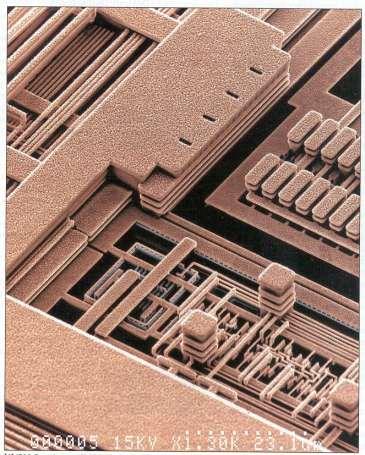
34 dvanced Metallization

35 From Design to Reality
36 Design Rules

37 CMOS Process Layers Layer Well (p,n) ctive rea (n+,p+) Select (p+,n+) Polysilicon Metal1 Metal2 Contact To Poly Contact To Diffusion Via Color Yellow Green Green Red lue Magenta lack lack lack Representation

38 Layers in 0.25 mm CMOS process
39 Design Rules Interface between the circuit designer and process engineer Guidelines for constructing process masks Unit dimension: minimum line width» scalable design rules: lambda parameter» absolute dimensions: micron rules Rules constructed to ensure that design works even when small fab errors (within some tolerance) occur complete set includes» set of layers» intra-layer: relations between objects in the same layer» inter-layer: relations between objects on different layers

40 3D Perspective Polysilicon luminum
41 Why Have Design Rules? To be able to tolerate some level of fabrication errors such as 1. Mask misalignment 2. Dust 3. Process parameters (e.g., lateral diffusion) 4. Rough surfaces
42 Intra-Layer Design Rule Origins Minimum dimensions (e.g., widths) of objects on each layer to maintain that object after fab» minimum line width is set by the resolution of the patterning process (photolithography) Minimum spaces between objects (that are not related) on the same layer to ensure they will not short after fab 0.3 micron micron
43 Inter-Layer Design Rule Origins 1. Transistor rules transistor formed by overlap of active and poly layers Transistors Catastrophic error Unrelated Poly & Diffusion Thinner diffusion, but still working
44 Inter-Layer Design Rule Origins, Con t 2. Contact and via rules M1 contact to p-diffusion M1 contact to n-diffusion M1 contact to poly Mx contact to My Contact Mask Via Masks both materials 0.3 Contact: 0.44 x 0.44 mask misaligned 0.14
45 Intra-Layer Design Rules Same Potential Different Potential Well 10 0 or 6 9 Polysilicon 2 2 ctive Select Contact or Via Hole 2 2 Metal1 Metal
46 Transistor Layout Transistor
47 Vias and Contacts 2 1 Via Metal to ctive Contact 1 Metal to Poly Contact
48 Select Layer Select Substrate Well
49 IC Layout
50 CMOS Inverter Sticks Diagram V DD 3 In 1 Out Dimensionless layout entities Only topology is important Final layout generated by compaction program GND Stick diagram of inverter
 NMOS (2/.")
51 CMOS Inverter max Layout metal1 metal2 Out In metal1-poly via polysilicon V DD pfet pdif metal1-diff via GND PMOS (4/.24 = 16/1) NMOS (2/.24 = 8/1) ndif nfet metal2-metal1 via

52 Layout Editor

53 Design Rule Checker poly_not_fet to all_diff minimum spacing = 0.14 um.

54 CMOS Inverters PMOS V DD In Out 1.2 mm =2l Metal1 Polysilicon NMOS GND

55 Layout Design Rule Violation Well-well spacing = 9 M1width = 4 M1- M1 spacing = 3 ctive to well edge = 5 Min active width = 3 Poly overlap of active = 2 M2 - M2 spacing = 4 ll distances in l
56 uilding an Inverter Step 1 Step 2 Step 3 Step 4 VCC P VCC Output P diffusion N diffusion Output N VSS Output VSS With permission of William radbury
57 uilding a 2 Input NOR Gate Out P Output Shared node P N N Step 1 Step 3 O u t p u t O u t p u t S h a r e d n o d e V S S V C C V S S Step 2 P N Step 4 V S S O u t p u t V C C With permission of William radbury
58 uilding a 2 Input NND Gate With permission of William radbury Step 1 Step 3 O u t p u t O u t p u t S h a r e d n o d e V S S V C C V S S Step 2 P N Step 4 V S S O u t p u t V C C Shared node Output P P N N Out
59 Combining Logic Functions Out VCC VCC VCC P P Out Out N Out VSS VSS N VSS With permission of William radbury
60 Cell Symbol to Logic to Transistor Schematic to Layout LD LD SRM IT TRNSISTOR SCHEMTIC INPUT SRM OUTPUT INPUT LD P2, 1.8 P4, 2.0 OUTPUT P1, 1.4 N1, 1.4 LD N2, 2.0 N4, 2.0 SRM IT LOGIC P3,.5/1.0 INPUT LD P 1.8 N 2.0 OUTPUT N3,.6/1.0 P 1.4 N 1.4 LD P 2.0 N 2.0 P.5/1.0 N.6/1.0 Minimum poly width L = 0.20 Note the listing of the L dimension which is not the minimum defined by the process With permission of William radbury
61 Schematic to Transistor LD OUTPUT P1 INPUT P2 VCC P4 VCC N1 INPUT N2 OUTPUT VSS N4 VSS LD N3 VSS P3 VCC With permission of William radbury
62 ssembling the Transistors by Type and Node Name INPUT LD VCC OUTPUT VCC VC C INPUT VSS OUTPUT LD VSS VSS With permission of William radbury
63 Connecting the Nodes INPUT LD VCC OUTPUT VCC VC C INPUT VSS OUTPUT LD VSS VSS With permission of William radbury
64 Connecting the Dotes VC C I N P U T LD V C C V C C O U T P U T UNMERGED DT: INPUT Notice the addition of contacts where necessary and also the use of redundant contacts to improve reliability I N P U T LD V S S VSS V SS O U T P U T With permission of William radbury
65 Cleaning Connections and Completing the layout. dded: 1.Taps 2.Implants 3.Cell boundry N-WELL P-IMPLNT LD DD IN P U T P1 P 3 P2 V C C V C C VC C P4 N-TP O U T P U T INPUT IN PU T LD N-IMPLNT VS S VS S VS S N1 N3 N4 N2 OUTPUT OU TP UT With permission of William radbury P-TP
66 . Using sticks VCC Metal1 P diffusion Output N diffusion Poly Contact VSS With permission of William radbury
67 Same cell, different shape. VCC VCC Output VCC VCC Out VSS Out VSS VSS With permission of William radbury
68 Cells Designed for Sharing. Sense Ckt. for One Row Memory Row 1 Reference Voltage Compare Row 1 Height of 1 Memory it 1 it 1 it Dual Sense mp Cell Height Memory Row 1 Reference Voltage Compare Row 1 Compare Row 2 Reference Voltage Memory Row 2 1 it 1 it Dual Sense mps Dual Write Line Ckts Courtesy Mentor Graphics Corp. Layout created using IC-Station. With permission of William radbury

69 Cells Designed for Sharing. With permission of William radbury
70 Packaging
 Cooling from back of chip High inductance (~1nH) More about packaging: http://www.embeddedlinks.com/chipdir/package.")
71 Packaging Requirements Desired package properties Electrical: Low parasitics Mechanical: Reliable and robust Thermal: Efficient heat removal Economical: Cheap Wire bonding Only periphery of chip available for IO connections Mechanical bonding of one pin at a time (sequential) Cooling from back of chip High inductance (~1nH) More about packaging:

 Cooling via balls")

72 Chip to package connection Flip-chip Whole chip area available for IO connections utomatic alignment One step process (parallel) Cooling via balls (front) and back if required Thermal matching between chip and substrate required Low inductance (~0.1nH)
73 onding Techniques Wire onding Substrate Die Pad Lead Frame
74 Tape-utomated onding (T) Sprocket hole Film + Pattern Solder ump Test pads Die Lead frame Substrate (b) Die attachment using solder bumps. (a) Polymer Tape with imprinted wiring pattern. Polymer film
 Small solder balls to")


75 New package types G (all Grid rray) Small solder balls to connect to board small High pin count Cheap Low inductance CSP (Chip scale Packaging) Similar to G Very small packages Package inductance: 1-5 nh

76 Flip-Chip onding Die Solder bumps Interconnect layers Substrate
77 Package-to-oard Interconnect (a) Through-Hole Mounting (b) Surface Mount

78 Package Types Through-hole vs. surface mount From dnan ziz
79 Chip-to-Package onding Traditionally, chip is surrounded by pad frame» Metal pads on mm pitch» Gold bond wires attach pads to package» Lead frame distributes signals in package» Metal heat spreader helps with cooling From dnan ziz
80 dvanced Packages ond wires contribute parasitic inductance Fancy packages have many signal, power layers» Like tiny printed circuit boards Flip-chip places connections across surface of die rather than around periphery» Top level metal pads covered with solder balls» Chip flips upside down» Carefully aligned to package (done blind!)» Heated to melt balls» lso called C4 (Controlled Collapse Chip Connection) From dnan ziz
81 Signal Pads Signal Pins Package Parasitics Use many V DD, GND in parallel» Inductance, I DD Package Chip V DD ond Wire Lead Frame oard V DD Chip Package Capacitor Chip GND oard GND From dnan ziz
82 Signal Interface Transfer of IC signals to PC» Package inductance.» PC wire capacitance.» L - C resonator circuit generating oscillations.» Transmission line effects may generate reflections» Cross-talk via mutual inductance L-C Oscillation Chip L PC trace Z f =1/(2p(LC) 1/2 ) L = 10 nh C = 10 pf f = ~500MHz C R Transmission line reflections Package
83 Package Parameters
84 Package Parameters
85 Package Parameters 2000 Summary of Intel s Package I/O Lead Electrical Parasitics for Multilayer Packages
")
86 Packaging Faults Small all Chip Scale Packages (CSP) Open

87 Packaging Faults CSP ssembly on 6 mil Via in 12 mil pad Void over via structure

88 Miniaturisation of Electronic Systems Enabling Technologies :»SOC»High Density Interconnection technologies SIP System-in-a-package From ECE 407/507 University of rizona

89 The Interconnection gap Improvement in density of standard interconnection and packaging technologies is much slower than the IC trends PC scaling dvanced PC Laser via IC scaling Interconnect Gap Time From ECE 407/507 University of rizona
90 The Interconnection gap Requires new high density Interconnect technologies PC scaling dvanced PC IC scaling Thin film lithography based Interconnect technology Reduced Gap Time From ECE 407/507 University of rizona

91 SoC has to overcome» Technical Challenges: Increased System Complexity. Integration of heterogeneous IC technologies. Lack of design and test methodologies.» usiness Challenges:» Solution Long Design and test cycles High risk investment Hence time to market. System-in-a-Package From ECE 407/507 University of rizona
92 Multi-Chip Modules
 Decrease loading of")


93 Multiple Chip Module (MCM) Increase integration level of system (smaller size) Decrease loading of external signals > higher performance No packaging of individual chips Problems with known good die:» Single chip fault coverage: 95%» MCM yield with 10 chips: (0.95) 10 = 60% Problems with cooling Still expensive

94 Complete PC in MCM
Manufacturing Process
 Digital Integrated Circuits A Design Perspective Jan M. Rabaey Anantha Chandrakasan Borivoje Nikolic Manufacturing Process July 30, 2002 1 CMOS Process 2 A Modern CMOS Process gate-oxide TiSi 2 AlCu Tungsten
CMOS Manufacturing Process
 CMOS Manufacturing Process CMOS Process A Modern CMOS Process gate-oxide TiSi 2 AlCu Tungsten SiO 2 n+ p-well p-epi poly n-well p+ SiO 2 p+ Dual-Well Trench-Isolated CMOS Process Circuit Under Design V
Lecture 1A: Manufacturing& Layout
 Introduction to CMOS VLSI Design Lecture 1A: Manufacturing& Layout David Harris Harvey Mudd College Spring 2004 Steven Levitan Fall 2008 1 The Manufacturing Process For a great tour through the IC manufacturing
CMOS Manufacturing process. Circuit designer. Design rule set. Process engineer. Set of optical masks. Fabrication process.
 CMOS Manufacturing process Circuit design Set of optical masks Fabrication process Circuit designer Design rule set Process engineer All material: Chap. 2 of J. Rabaey, A. Chandrakasan, B. Nikolic, Digital
FABRICATION of MOSFETs
 FABRICATION of MOSFETs CMOS fabrication sequence -p-type silicon substrate wafer -creation of n-well regions for pmos transistors, -impurity implantation into the substrate. -thick oxide is grown in the
Cost of Integrated Circuits
 Cost of IC Design 1 Cost of Integrated Circuits NRE (Non-Recurrent Engineering) costs fixed design time and effort, mask generation independent of sales volume / number of products one-time cost factor
VLSI INTRODUCTION P.VIDYA SAGAR ( ASSOCIATE PROFESSOR) Department of Electronics and Communication Engineering, VBIT
 Department of Electronics and Communication Engineering, VBIT") VLSI INTRODUCTION P.VIDYA SAGAR ( ASSOCIATE PROFESSOR) contents UNIT I INTRODUCTION: Introduction to IC Technology MOS, PMOS, NMOS, CMOS & BiCMOS technologies. BASIC ELECTRICAL PROPERTIES : Basic Electrical
VLSI INTRODUCTION P.VIDYA SAGAR ( ASSOCIATE PROFESSOR) contents UNIT I INTRODUCTION: Introduction to IC Technology MOS, PMOS, NMOS, CMOS & BiCMOS technologies. BASIC ELECTRICAL PROPERTIES : Basic Electrical
Introduction to CMOS VLSI Design. Layout, Fabrication, and Elementary Logic Design
 Introduction to CMOS VLSI Design Layout, Fabrication, and Elementary Logic Design CMOS Fabrication CMOS transistors are fabricated on silicon wafer Lithography process similar to printing press On each
CMOS VLSI Design. Introduction. All materials are from the textbook Weste and Harris, 3 rd Edition CMOS VLSI DESIGN. Introduction
 CMOS VLSI Design Introduction ll materials are from the textbook Weste and Harris, 3 rd Edition CMOS VLSI DESIGN Introduction Chapter previews the entire field, subsequent chapters elaborate on specific
CMOS Fabrication. Dr. Bassam Jamil. Adopted from slides of the textbook
 CMOS Fabrication Dr. Bassam Jamil Adopted from slides of the textbook CMOS Fabrication CMOS transistors are fabricated on silicon wafer Lithography process similar to printing press On each step, different
Fabrication and Layout
 ECEN454 Digital Integrated Circuit Design Fabrication and Layout ECEN 454 3.1 A Glimpse at MOS Device Polysilicon Aluminum ECEN 475 4.2 1 Material Classification Insulators Glass, diamond, silicon oxide
UT Austin, ECE Department VLSI Design 2. CMOS Fabrication, Layout Rules
 2. CMOS Fabrication, Layout, Design Rules Last module: Introduction to the course How a transistor works CMOS transistors This module: CMOS Fabrication Design Rules CMOS Fabrication CMOS transistors are
Lecture 0: Introduction
 Lecture 0: Introduction Introduction Integrated circuits: many transistors on one chip. Very Large Scale Integration (VLSI): bucketloads! Complementary Metal Oxide Semiconductor Fast, cheap, low power
CMOS FABRICATION. n WELL PROCESS
 CMOS FABRICATION n WELL PROCESS Step 1: Si Substrate Start with p- type substrate p substrate Step 2: Oxidation Exposing to high-purity oxygen and hydrogen at approx. 1000 o C in oxidation furnace SiO
VLSI. Lecture 1. Jaeyong Chung System-on-Chips (SoC) Laboratory Incheon National University. Based on slides of David Money Harris
 Laboratory Incheon National University. Based on slides of David Money Harris") VLSI Lecture 1 Jaeyong Chung System-on-Chips (SoC) Laboratory Incheon National University Based on slides of David Money Harris Goals of This Course Learn the principles of VLSI design Learn to design
VLSI Lecture 1 Jaeyong Chung System-on-Chips (SoC) Laboratory Incheon National University Based on slides of David Money Harris Goals of This Course Learn the principles of VLSI design Learn to design
Fabrication and Layout
 Fabrication and Layout Kenneth Yun UC San Diego Adapted from EE271 notes, Stanford University Overview Semiconductor properties How chips are made Design rules for layout Reading Fabrication: W&E 3.1,
EE 330 Lecture 9. IC Fabrication Technology Part II. -Oxidation -Epitaxy -Polysilicon -Planarization -Resistance and Capacitance in Interconnects
 EE 330 Lecture 9 IC Fabrication Technology Part II -Oxidation -Epitaxy -Polysilicon -Planarization -Resistance and Capacitance in Interconnects Review from Last Time Etching Dry etch (anisotropic) SiO
Lecture 19 Microfabrication 4/1/03 Prof. Andy Neureuther
 EECS 40 Spring 2003 Lecture 19 Microfabrication 4/1/03 Prof. ndy Neureuther How are Integrated Circuits made? Silicon wafers Oxide formation by growth or deposition Other films Pattern transfer by lithography
EE 434 Lecture 9. IC Fabrication Technology
 EE 434 Lecture 9 IC Fabrication Technology Quiz 7 The layout of a film resistor with electrodes A and B is shown. If the sheet resistance of the film is 40 /, determine the resistance between nodes A and
VLSI Digital Systems Design
 VLSI Digital Systems Design CMOS Processing cmpe222_03process_ppt.ppt 1 Si Purification Chemical purification of Si Zone refined Induction furnace Si ingot melted in localized zone Molten zone moved from
Silicon Wafer Processing PAKAGING AND TEST
 Silicon Wafer Processing PAKAGING AND TEST Parametrical test using test structures regularly distributed in the wafer Wafer die test marking defective dies dies separation die fixing (not marked as defective)
Figure 2.3 (cont., p. 60) (e) Block diagram of Pentium 4 processor with 42 million transistors (2000). [Courtesy Intel Corporation.
 (e) Block diagram of Pentium 4 processor with 42 million transistors (2000). [Courtesy Intel Corporation.") Figure 2.1 (p. 58) Basic fabrication steps in the silicon planar process: (a) oxide formation, (b) selective oxide removal, (c) deposition of dopant atoms on wafer, (d) diffusion of dopant atoms into exposed
Figure 2.1 (p. 58) Basic fabrication steps in the silicon planar process: (a) oxide formation, (b) selective oxide removal, (c) deposition of dopant atoms on wafer, (d) diffusion of dopant atoms into exposed
EE40 Lec 22. IC Fabrication Technology. Prof. Nathan Cheung 11/19/2009
 Suggested Reading EE40 Lec 22 IC Fabrication Technology Prof. Nathan Cheung 11/19/2009 300mm Fab Tour http://www-03.ibm.com/technology/manufacturing/technology_tour_300mm_foundry.html Overview of IC Technology
EEC 118 Lecture #5: MOS Fabrication. Rajeevan Amirtharajah University of California, Davis Jeff Parkhurst Intel Corporation
 EEC 118 Lecture #5: MOS Fabrication Rajeevan Amirtharajah University of California, Davis Jeff Parkhurst Intel Corporation Announcements Lab 3 this week, report due next week HW 3 due this Friday at 4
VLSI Systems and Computer Architecture Lab
 ΚΥΚΛΩΜΑΤΑ VLSI Πανεπιστήμιο Ιωαννίνων CMOS Technology Τμήμα Μηχανικών Η/Υ και Πληροφορικής 1 From the book: An Introduction ti to VLSI Process By: W. Maly ΚΥΚΛΩΜΑΤΑ VLSI Διάρθρωση 1. N well CMOS 2. Active
Lecture 22: Integrated circuit fabrication
 Lecture 22: Integrated circuit fabrication Contents 1 Introduction 1 2 Layering 4 3 Patterning 7 4 Doping 8 4.1 Thermal diffusion......................... 10 4.2 Ion implantation.........................
Chapter 2 MOS Fabrication Technology
 Chapter 2 MOS Fabrication Technology Abstract This chapter is concerned with the fabrication of metal oxide semiconductor (MOS) technology. Various processes such as wafer fabrication, oxidation, mask
ECE520 VLSI Design. Lecture 7: CMOS Manufacturing Process. Payman Zarkesh-Ha
 ECE520 VLSI Design Lecture 7: CMOS Manufacturing Process Payman Zarkesh-Ha Office: ECE Bldg. 230B Office hours: Wednesday 2:00-3:00PM or by appointment E-mail: pzarkesh@unm.edu Slide: 1 Review of Last
Chapter 3 Silicon Device Fabrication Technology
 Chapter 3 Silicon Device Fabrication Technology Over 10 15 transistors (or 100,000 for every person in the world) are manufactured every year. VLSI (Very Large Scale Integration) ULSI (Ultra Large Scale
Analog Devices ADSP KS-160 SHARC Digital Signal Processor
 Construction Analysis Analog Devices ADSP-21062-KS-160 SHARC Digital Signal Processor Report Number: SCA 9712-575 Global Semiconductor Industry the Serving Since 1964 17350 N. Hartford Drive Scottsdale,
EE 560 FABRICATION OF MOS CIRCUITS. Kenneth R. Laker, University of Pennsylvania
 1 EE 560 FABRICATION OF MOS CIRCUITS 2 CMOS CHIP MANUFACTRING STEPS Substrate Wafer Wafer Fabrication (diffusion, oxidation, photomasking, ion implantation, thin film deposition, etc.) Finished Wafer Wafer
KGC SCIENTIFIC Making of a Chip
 KGC SCIENTIFIC www.kgcscientific.com Making of a Chip FROM THE SAND TO THE PACKAGE, A DIAGRAM TO UNDERSTAND HOW CPU IS MADE? Sand CPU CHAIN ANALYSIS OF SEMICONDUCTOR Material for manufacturing process
Motorola PC603R Microprocessor
 Construction Analysis Motorola PC603R Microprocessor Report Number: SCA 9709-551 Global Semiconductor Industry the Serving Since 1964 17350 N. Hartford Drive Scottsdale, AZ 85255 Phone: 602-515-9780 Fax:
Semiconductor Manufacturing Technology. IC Fabrication Process Overview
 Semiconductor Manufacturing Technology Michael Quirk & Julian Serda October 00 by Prentice Hall Chapter 9 IC Fabrication Process Overview /4 Objectives After studying the material in this chapter, you
Lecture 2. Fabrication and Layout
 Lecture 2 Fabrication and Layout Mark Horowitz Modified by Azita Emami Computer Systems Laboratory Stanford University azita@stanford.edu 1 Overview Reading W&E 3.1(scan), 3.2.1, 3.3.1 - Fabrication W&E
VLSI Technology. By: Ajay Kumar Gautam
 By: Ajay Kumar Gautam Introduction to VLSI Technology, Crystal Growth, Oxidation, Epitaxial Process, Diffusion Process, Ion Implantation, Lithography, Etching, Metallization, VLSI Process Integration,
Ajay Kumar Gautam [VLSI TECHNOLOGY] VLSI Technology for 3RD Year ECE/EEE Uttarakhand Technical University
![Ajay Kumar Gautam [VLSI TECHNOLOGY] VLSI Technology for 3RD Year ECE/EEE Uttarakhand Technical University](/thumbs/75/72824557.jpg "Ajay Kumar Gautam [VLSI TECHNOLOGY] VLSI Technology for 3RD Year ECE/EEE Uttarakhand Technical University") 2014 Ajay Kumar Gautam [VLSI TECHNOLOGY] VLSI Technology for 3RD Year ECE/EEE Uttarakhand Technical University Page1 Syllabus UNIT 1 Introduction to VLSI Technology: Classification of ICs, Scale of integration,
2014 Ajay Kumar Gautam [VLSI TECHNOLOGY] VLSI Technology for 3RD Year ECE/EEE Uttarakhand Technical University Page1 Syllabus UNIT 1 Introduction to VLSI Technology: Classification of ICs, Scale of integration,
Intel Pentium Processor W/MMX
 Construction Analysis Intel Pentium Processor W/MMX Report Number: SCA 9706-540 Global Semiconductor Industry the Serving Since 1964 15022 N. 75th Street Scottsdale, AZ 85260-2476 Phone: 602-998-9780 Fax:
Process Flow in Cross Sections
 Process Flow in Cross Sections Process (simplified) 0. Clean wafer in nasty acids (HF, HNO 3, H 2 SO 4,...) --> wear gloves! 1. Grow 500 nm of SiO 2 (by putting the wafer in a furnace with O 2 2. Coat
EECS130 Integrated Circuit Devices
 EECS130 Integrated Circuit Devices Professor Ali Javey 9/13/2007 Fabrication Technology Lecture 1 Silicon Device Fabrication Technology Over 10 15 transistors (or 100,000 for every person in the world)
Lecture 030 Integrated Circuit Technology - I (5/8/03) Page 030-1
 Page 030-1") Lecture 030 Integrated Circuit Technology - I (5/8/03) Page 030-1 LECTURE 030 INTEGRATED CIRCUIT TECHNOLOGY - I (References [7,8]) Objective The objective of this presentation is: 1.) Illustrate integrated
Lecture 030 Integrated Circuit Technology - I (5/8/03) Page 030-1 LECTURE 030 INTEGRATED CIRCUIT TECHNOLOGY - I (References [7,8]) Objective The objective of this presentation is: 1.) Illustrate integrated
The Physical Structure (NMOS)
") The Physical Structure (NMOS) Al SiO2 Field Oxide Gate oxide S n+ Polysilicon Gate Al SiO2 SiO2 D n+ L channel P Substrate Field Oxide contact Metal (S) n+ (G) L W n+ (D) Poly 1 3D Perspective 2 3 Fabrication
The Physical Structure (NMOS) Al SiO2 Field Oxide Gate oxide S n+ Polysilicon Gate Al SiO2 SiO2 D n+ L channel P Substrate Field Oxide contact Metal (S) n+ (G) L W n+ (D) Poly 1 3D Perspective 2 3 Fabrication
THE MANUFACTURING PROCESS
 chapter2.fm Page 33 Monday, September 4, 2000 11:11 AM CHAPTER 2 THE MANUFACTURING PROCESS Overview of manufacturing process n Design rules n IC packaging n Future Trends in Integrated Circuit Technology
Fabrication Process. Crystal Growth Doping Deposition Patterning Lithography Oxidation Ion Implementation CONCORDIA VLSI DESIGN LAB
 Fabrication Process Crystal Growth Doping Deposition Patterning Lithography Oxidation Ion Implementation 1 Fabrication- CMOS Process Starting Material Preparation 1. Produce Metallurgical Grade Silicon
Hitachi A 64Mbit (8Mb x 8) Dynamic RAM
 Dynamic RAM") Construction Analysis Hitachi 5165805A 64Mbit (8Mb x 8) Dynamic RAM Report Number: SCA 9712-565 Global Semiconductor Industry the Serving Since 1964 17350 N. Hartford Drive Scottsdale, AZ 85255 Phone:
Construction Analysis Hitachi 5165805A 64Mbit (8Mb x 8) Dynamic RAM Report Number: SCA 9712-565 Global Semiconductor Industry the Serving Since 1964 17350 N. Hartford Drive Scottsdale, AZ 85255 Phone:
Isolation Technology. Dr. Lynn Fuller
 ROCHESTER INSTITUTE OF TECHNOLOGY MICROELECTRONIC ENGINEERING Isolation Technology Dr. Lynn Fuller Motorola Professor 82 Lomb Memorial Drive Rochester, NY 14623-5604 Tel (585) 475-2035 Fax (585) 475-5041
Rockwell R RF to IF Down Converter
 Construction Analysis Rockwell R6732-13 RF to IF Down Converter Report Number: SCA 9709-552 Global Semiconductor Industry the Serving Since 1964 17350 N. Hartford Drive Scottsdale, AZ 85255 Phone: 602-515-9780
CSCI 4974 / 6974 Hardware Reverse Engineering. Lecture 5: Fabrication processes
 CSCI 4974 / 6974 Hardware Reverse Engineering Lecture 5: Fabrication processes QUIZ 3: CMOS layout Quiz Discussion Rationale If you know how something is put together, you can figure out how to take it
Dallas Semicoductor DS80C320 Microcontroller
 Construction Analysis Dallas Semicoductor DS80C320 Microcontroller Report Number: SCA 9702-525 Global Semiconductor Industry the Serving Since 1964 15022 N. 75th Street Scottsdale, AZ 85260-2476 Phone:
Process Integration. NMOS Generic NMOS Process Flow. CMOS - The MOSIS Process Flow
 Process Integration Self-aligned Techniques LOCOS- self-aligned channel stop Self-aligned Source/Drain Lightly Doped Drain (LDD) Self-aligned silicide (SALICIDE) Self-aligned oxide gap MEMS Release Techniques
Semiconductor Device Fabrication
 5 May 2003 Review Homework 6 Semiconductor Device Fabrication William Shockley, 1945 The network before the internet Bell Labs established a group to develop a semiconductor replacement for the vacuum
Historical Development. Babbage s second computer. Before the digital age
 Historical Development To fully appreciate the computers of today, it is helpful to understand how things got the way they are The evolution of computing machinery has taken place over several centuries
1 Thin-film applications to microelectronic technology
 1 Thin-film applications to microelectronic technology 1.1 Introduction Layered thin-film structures are used in microelectronic, opto-electronic, flat panel display, and electronic packaging technologies.
SGS-Thomson M17C1001 1Mb UVEPROM
 Construction Analysis SGS-Thomson M17C1001 1Mb UVEPROM Report Number: SCA 9612-518 Global Semiconductor Industry the Serving Since 1964 15022 N. 75th Street Scottsdale, AZ 85260-2476 Phone: 602-998-9780
PROCESSING OF INTEGRATED CIRCUITS
 PROCESSING OF INTEGRATED CIRCUITS Overview of IC Processing (Part I) Silicon Processing Lithography Layer Processes Use in IC Fabrication (Part II) Integrating the Fabrication Steps IC Packaging (Part
HOMEWORK 4 and 5. March 15, Homework is due on Monday March 30, 2009 in Class. Answer the following questions from the Course Textbook:
 HOMEWORK 4 and 5 March 15, 2009 Homework is due on Monday March 30, 2009 in Class. Chapter 7 Answer the following questions from the Course Textbook: 7.2, 7.3, 7.4, 7.5, 7.6*, 7.7, 7.9*, 7.10*, 7.16, 7.17*,
Lattice isplsi1032e CPLD
 Construction Analysis Lattice isplsi1032e CPLD Report Number: SCA 9612-522 Global Semiconductor Industry the Serving Since 1964 15022 N. 75th Street Scottsdale, AZ 85260-2476 Phone: 602-998-9780 Fax: 602-948-1925
ELEC 3908, Physical Electronics, Lecture 4. Basic Integrated Circuit Processing
 ELEC 3908, Physical Electronics, Lecture 4 Basic Integrated Circuit Processing Lecture Outline Details of the physical structure of devices will be very important in developing models for electrical behavior
Modeling of Local Oxidation Processes
 Introduction Isolation Processes in the VLSI Technology Main Aspects of LOCOS simulation Athena Oxidation Models Several Examples of LOCOS structures Calibration of LOCOS effects using VWF Field Oxide
National Semiconductor LM2672 Simple Switcher Voltage Regulator
 Construction Analysis National Semiconductor LM2672 Simple Switcher Voltage Regulator Report Number: SCA 9712-570 Global Semiconductor Industry the Serving Since 1964 17350 N. Hartford Drive Scottsdale,
CHAPTER 1 HOW SEMICONDUCTOR CHIPS ARE MADE
 CHAPTER 1 HOW SEMICONDUCTOR CHIPS ARE MADE Hwaiyu Geng Hewlett-Packard Company Palo Alto, California Lin Zhou Intel Corporation Hillsboro, Oregon 1.1 INTRODUCTION Over the past decades, an information
Is Now Part of To learn more about ON Semiconductor, please visit our website at
 Is Now Part of To learn more about ON Semiconductor, please visit our website at www.onsemi.com ON Semiconductor and the ON Semiconductor logo are trademarks of Semiconductor Components Industries, LLC
Chapter 2 Problems. The CMOS technology we need to realize is shown below, from Figure 1-34 in the text. S P + N P + N WELL P +
 Chapter 2 roblems 2.1 Sketch a process flow that would result in the structure shown in Figure 1-34 by drawing a series of drawings similar to those in this chapter. You only need to describe the flow
Fabrication Technology
 Fabrication Technology By B.G.Balagangadhar Department of Electronics and Communication Ghousia College of Engineering, Ramanagaram 1 OUTLINE Introduction Why Silicon The purity of Silicon Czochralski
TSV Processing and Wafer Stacking. Kathy Cook and Maggie Zoberbier, 3D Business Development
 TSV Processing and Wafer Stacking Kathy Cook and Maggie Zoberbier, 3D Business Development Outline Why 3D Integration? TSV Process Variations Lithography Process Results Stacking Technology Wafer Bonding
EE 330 Fall Ruden Michael. Al Kaabi Humaid. Archer Tyler. Hafeez Mustafa. Mullen Taylor. Thedens Peter. Cao Khoi.
 1 2 5 6 3 4 8 7 1 2 3 4 5 6 ROW EE 330 Fall 2017 9 10 Al Kaabi Humaid Alegria Francisco Allison Trenton Alva Caroline Archer Tyler Bahashwan Abdullah Betke Jarrett Chun Junho Davidson Caleb Faronbi Matthew
Metallization deposition and etching. Material mainly taken from Campbell, UCCS
 Metallization deposition and etching Material mainly taken from Campbell, UCCS Application Metallization is back-end processing Metals used are aluminum and copper Mainly involves deposition and etching,
HYPRES. Hypres MCM Process Design Rules 04/12/2016
 HYPRES Hypres MCM Process Design Rules 04/12/2016 Direct all inquiries, questions, comments and suggestions concerning these design rules and/or HYPRES fabrication to: Daniel T. Yohannes Tel. (914) 592-1190
4/10/2012. Introduction to Microfabrication. Fabrication
 Introduction to Microfabrication Fabrication 1 MEMS Fabrication Flow Basic Process Flow in Micromachining Nadim Maluf, An introduction to Microelectromechanical Systems Engineering 2 Thin Film Deposition
Technology. Semiconductor Manufacturing. Hong Xiao INTRODUCTION TO SECOND EDITION SPIE PRESS
 INTRODUCTION TO Semiconductor Manufacturing Technology SECOND EDITION Hong Xiao TECHNISCHE INFORMATIONSBiBUOTHEK UNIVERSITATSBIBLIOTHEK HANNOVER SPIE PRESS Bellingham,Washington USA Contents Preface to
3.155J / 6.152J Micro/Nano Processing Technology TAKE-HOME QUIZ FALL TERM 2005
 3.155J / 6.152J Micro/Nano Processing Technology TAKE-HOME QUIZ FALL TERM 2005 1) This is an open book, take-home quiz. You are not to consult with other class members or anyone else. You may discuss the
MOS Front-End. Field effect transistor
 MOS Front-End Back-end Transistor Contact Front-end p-well STI n-well Front-end-of-line includes substrate, isolation, wells, transistor, silicide Field effect transistor MOSFET: Metal-Oxide-Semiconductor
PHYSICAL ELECTRONICS(ECE3540) Brook Abegaz, Tennessee Technological University, Fall 2013
 Brook Abegaz, Tennessee Technological University, Fall 2013") PHYSICAL ELECTRONICS(ECE3540) Brook Abegaz, Tennessee Technological University, Fall 2013 1 Chapter 1 The Crystal Structure of Solids Physical Electronics: Includes aspects of the physics of electron movement
PHYSICAL ELECTRONICS(ECE3540) Brook Abegaz, Tennessee Technological University, Fall 2013 1 Chapter 1 The Crystal Structure of Solids Physical Electronics: Includes aspects of the physics of electron movement
A discussion of crystal growth, lithography, etching, doping, and device structures is presented in
 Chapter 5 PROCESSING OF DEVICES A discussion of crystal growth, lithography, etching, doping, and device structures is presented in the following overview gures. SEMICONDUCTOR DEVICE PROCESSING: AN OVERVIEW
FABRICATION ENGINEERING MICRO- NANOSCALE ATTHE AND. Fourth Edition STEPHEN A. CAMPBELL. of Minnesota. University OXFORD UNIVERSITY PRESS
 AND FABRICATION ENGINEERING ATTHE MICRO- NANOSCALE Fourth Edition STEPHEN A. CAMPBELL University of Minnesota New York Oxford OXFORD UNIVERSITY PRESS CONTENTS Preface xiii prrt i OVERVIEW AND MATERIALS
Silicon Manufacturing
 Silicon Manufacturing Group Members Young Soon Song Nghia Nguyen Kei Wong Eyad Fanous Hanna Kim Steven Hsu th Fundamental Processing Steps 1.Silicon Manufacturing a) Czochralski method. b) Wafer Manufacturing
VLSI Technology Dr. Nandita Dasgupta Department of Electrical Engineering Indian Institute of Technology, Madras
 VLSI Technology Dr. Nandita Dasgupta Department of Electrical Engineering Indian Institute of Technology, Madras Lecture - 33 Problems in LOCOS + Trench Isolation and Selective Epitaxy So, we are discussing
Surface micromachining and Process flow part 1
 Surface micromachining and Process flow part 1 Identify the basic steps of a generic surface micromachining process Identify the critical requirements needed to create a MEMS using surface micromachining
6.777J/2.732J Design and Fabrication of Microelectromechanical Devices Spring Term Solution to Problem Set 2 (16 pts)
") 6.777J/2.732J Design and Fabrication of Microelectromechanical Devices Spring Term 2007 By Brian Taff (Adapted from work by Feras Eid) Solution to Problem Set 2 (16 pts) Issued: Lecture 4 Due: Lecture
6.777J/2.732J Design and Fabrication of Microelectromechanical Devices Spring Term 2007 By Brian Taff (Adapted from work by Feras Eid) Solution to Problem Set 2 (16 pts) Issued: Lecture 4 Due: Lecture
Doping and Oxidation
 Technische Universität Graz Institute of Solid State Physics Doping and Oxidation Franssila: Chapters 13,14, 15 Peter Hadley Technische Universität Graz Institute of Solid State Physics Doping Add donors
A New High-k Transistor Technology Implemented in Accordance with the 55nm Design Rule Process
 A New High-k Transistor Technology Implemented in Accordance with the 55nm Design Rule Process FUKASE Tadashi, NAKAHARA Yasushi, TAKAHASHI Toshifumi, IMAI Kiyotaka Abstract NEC Electronics has developed
Thin Films: Sputtering Systems (Jaeger Ch 6 & Ruska Ch 7,) Can deposit any material on any substrate (in principal) Start with pumping down to high
 Can deposit any material on any substrate (in principal) Start with pumping down to high") Thin Films: Sputtering Systems (Jaeger Ch 6 & Ruska Ch 7,) Can deposit any material on any substrate (in principal) Start with pumping down to high vacuum ~10-7 torr Removes residual gases eg oxygen from
Thin Films: Sputtering Systems (Jaeger Ch 6 & Ruska Ch 7,) Can deposit any material on any substrate (in principal) Start with pumping down to high vacuum ~10-7 torr Removes residual gases eg oxygen from
Thin Films: Sputtering Systems (Jaeger Ch 6 & Ruska Ch 7,) Sputtering: gas plasma transfers atoms from target to substrate Can deposit any material
 Sputtering: gas plasma transfers atoms from target to substrate Can deposit any material") Thin Films: Sputtering Systems (Jaeger Ch 6 & Ruska Ch 7,) Sputtering: gas plasma transfers atoms from target to substrate Can deposit any material on any substrate (in principal) Start with pumping down
Thin Films: Sputtering Systems (Jaeger Ch 6 & Ruska Ch 7,) Sputtering: gas plasma transfers atoms from target to substrate Can deposit any material on any substrate (in principal) Start with pumping down
Welcome MNT Conference 1 Albuquerque, NM - May 2010
 Welcome MNT Conference 1 Albuquerque, NM - May 2010 Introduction to Design Outline What is MEMs Design General Considerations Application Packaging Process Flow What s available Sandia SUMMiT Overview
Cambridge University Press A Guide to Hands-on MEMS Design and Prototyping Joel A. Kubby Excerpt More information.
 1 Introduction 1.1 Overview of MEMS fabrication Microelectromechanical systems (MEMS) fabrication developed out of the thin-film processes first used for semiconductor fabrication. To understand the unique
Lecture 7 CMOS MEMS. CMOS MEMS Processes. CMOS MEMS Processes. Why CMOS-MEMS? Agenda: CMOS MEMS: Fabrication. MEMS structures can be made
 EEL6935 Advanced MEMS (Spring 2005) Instructor: Dr. Huikai Xie CMOS MEMS Agenda: Lecture 7 CMOS MEMS: Fabrication Pre-CMOS Intra-CMOS Post-CMOS Deposition Etching Why CMOS-MEMS? Smart on-chip CMOS circuitry
Chapter 2 Capacitive Sensing Electrodes
 Chapter 2 Capacitive Sensing Electrodes The capacitive sensing electrodes on the top of a CMOS chip serve as an interface between the microelectronic readout system and the biological/chemical analyte.
Interconnects OUTLINE
 Interconnects 1 Interconnects OUTLINE 1. Overview of Metallization 2. Introduction to Deposition Methods 3. Interconnect Technology 4. Contact Technology 5. Refractory Metals and their Silicides Reading:
Today s Class. Materials for MEMS
 Lecture 2: VLSI-based Fabrication for MEMS: Fundamentals Prasanna S. Gandhi Assistant Professor, Department of Mechanical Engineering, Indian Institute of Technology, Bombay, Recap: Last Class What is
Plasma Etching Rates & Gases Gas ratios affects etch rate & etch ratios to resist/substrate
 Plasma Etching Rates & Gases Gas ratios affects etch rate & etch ratios to resist/substrate Development of Sidewalls Passivating Films Sidewalls get inert species deposited on them with plasma etch Creates
TANOS Charge-Trapping Flash Memory Structures
 TANOS Charge-Trapping Flash Memory Structures A Senior Design by Spencer Pringle 5/8/15 Table of Contents Motivation Why Charge-Trapping Flash (CTF)? Charge-Trapping vs. Floating Gate Electronically-Erasable
Semiconductor Technology
 Semiconductor Technology von A bis Z Metallization www.halbleiter.org Contents Contents List of Figures List of Tables II III 1 Metallization 1 1.1 Requirements on metallization........................
Semiconductor Physics Course Final Presentation CMOS Fabrication by Özgür Çobanoğlu (Turin, 2006)
") Semiconductor Physics Course Final Presentation CMOS Fabrication by Özgür Çobanoğlu (Turin, 2006) 1 Outline Sections and Contents of the Presentation What is MOS? How does MOS behave in low level? A useful
Semiconductor Physics Course Final Presentation CMOS Fabrication by Özgür Çobanoğlu (Turin, 2006) 1 Outline Sections and Contents of the Presentation What is MOS? How does MOS behave in low level? A useful
Radiation Tolerant Isolation Technology
 Radiation Tolerant Isolation Technology Background The following contains a brief description of isolation technologies used for radiation hardened integrated circuits. The technologies mentioned are junction
Surface Micromachining
 Surface Micromachining Outline Introduction Material often used in surface micromachining Material selection criteria in surface micromachining Case study: Fabrication of electrostatic motor Major issues
Wafer Process. For University Ver1.1. October, Renesas Technology Corp., All rights reserved.
 Wafer Process Overseas Design Support Center Shigeru Shimada October, 2007 For University Ver1.1 Contents of Wafer Process 1. What is semiconductor? 2. Why silicon is mot popular? 3. N type and P type
CMOS VLSI Design M.Tech. First semester VTU Anil V. Nandi, ECE department, BVBCET, Hubli
 CMOS VLSI Design M.Tech. First semester VTU Anil V. Nandi, ECE department, BVBCET, Hubli-580031. Contents: Semiconductor Technology overview Silicon Growth/Processing,Oxidation, Diffusion, Epitaxy, deposition,
New Materials as an enabler for Advanced Chip Manufacturing
 New Materials as an enabler for Advanced Chip Manufacturing Drive Innovation, Deliver Excellence ASM International Analyst and Investor Technology Seminar Semicon West July 10 2013 Outline New Materials:
Leveraging the Precision of Electroforming over Alternative Processes When Developing Nano-scale Structures
 VOLUME 4 - ELECTROFORMING Leveraging the Precision of over Alternative Processes When Developing Nano-scale Structures Electrical and mechanical component and subsystem designers generally have five techniques