Altera EPM7128SQC EPLD
|
|
|
- Horatio Fleming
- 5 years ago
- Views:
Transcription
1 Construction Analysis Altera EPM7128SQC EPLD Report Number: SCA Global Semiconductor Industry the Serving Since N. Hartford Drive Scottsdale, AZ Phone: Fax: Internet:
2 INDEX TO TEXT TITLE PAGE INTRODUCTION 1 MAJOR FINDINGS 1 TECHNOLOGY DESCRIPTION Packaging/Assembly 2 Die Process 2-3 ANALYSIS RESULTS I Assembly 4 ANALYSIS RESULTS II Die Process 5-7 TABLES Procedure 8 Overall Quality Evaluation 9 Package Markings 10 Die Material Analysis 10 Horizontal Dimensions 11 Vertical Dimensions 12 i
3 INTRODUCTION This report describes a construction analysis of the Altera EPM7128SQC PLD. One device packaged in 160-pin PQFP (plastic quad flat pack) with gull-wing leads for surface mount applications was provided. The part was date coded MAJOR FINDINGS Questionable Items: 1 None. Special Features: Two-metal, twin-well, CMOS process. EEPROM cell programming with tunnel oxide windows for programming. Sub-micron gates (0.55 micron N-channel, 0.8 micron P-channel). 1 These items present possible quality or reliability concerns. They should be discussed with the manufacturer to determine their possible impact on the intended application
4 TECHNOLOGY DESCRIPTION Packaging/Assembly: Device was encapsulated in a 160-pin plastic quad flat pack with gull-wing leads. Lead-locking provisions (anchors) at all pins and (holes) in paddle tie bar. Dimpled paddle for additional package strength. Sawn dicing (full depth). Silver (Ag) epoxy die attach. Die Process: Fabrication: Twin-well, CMOS, P substrate, selective oxidation process. No epi. Final passivation: A layer of silicon-nitride over silicon-dioxide. Metallization: Two levels of aluminum interconnect patterned by dry-etch techniques. A titanium-nitride (TiN) cap metal and a titanium-tungsten (TiW) barrier metal were employed with both metal levels. The aluminum layers were silicon doped but no copper was detected. Interlevel dielectric: Two layers of silicon-dioxide. A spin-on-glass (SOG) was used between these layers for planarization purposes. The first layer of silicon dioxide appeared to be undoped. No evidence of chemical-mechanical-planarization (CMP) was present. Pre-metal glass: A BPSG reflow glass over various densified oxides. It appeared to have been reflowed prior to contact cuts only. Polysilicon: A single layer of dry etched polycide (tungsten silicide on poly) formed all gates on the die
5 TECHNOLOGY DESCRIPTION (continued) Diffusions: Transistors were formed using an LDD process in which the oxide sidewall spacers were left in place. Implanted N+ and P+ sources/drains. Twin-wells were used in a P substrate. No epi was present. No buried contacts were employed on this device. Memory cells: The programmable array consisted of EEPROM cells (E 2 CMOS process). Metal 2 was used to form "piggyback" word lines. Metal 1 formed the bit 1, bit 2, enable and word interconnect lines. Poly formed the word lines, all gates and one plate of the capacitor. A thin tunnel-oxide window was utilized in the cell design. An N+ implant was present beneath the tunnel oxide device
6 ANALYSIS RESULTS I Assembly : Figures 1-2 Questionable Items: None. General Items: 160-pin PQFP packages with gull-wing leads. Overall package quality: Normal. No serious defects were found on the external or internal portions of the package. Leadframe: Lead-locking provisions (anchors) were present at all pins (holes) were present in the header tie bar. Paddle: A dimpled paddle was employed for additional package strength. Die attach: The die was attached to the paddle with silver-epoxy of good quality. Die dicing: Die separation was by sawing with normal quality workmanship. No cracks or large chipouts were found in the die
7 ANALYSIS RESULTS II Die Process : Figures 3-29 Questionable Items: 1 None. Special Features: Two-metal, twin-well, CMOS process. EEPROM cell programming with tunnel oxide windows for programming. Sub-micron gates (0.55 micron N-channel, 0.8 micron P-channel). General Items: Fabrication process: Selective oxidation CMOS using twin-wells in a P substrate. No epi was present. Process Implementation: Die layout was clean and efficient. Alignment/registration was good at all levels and no damage or contamination was found. Final passivation: A layer of silicon-nitride over silicon-dioxide. Passivation extended in scribe lane covering all metal lines. Metallization: Two levels of silicon-doped aluminum interconnect (no copper detected). A titanium-nitride (TiN) cap metal and a titanium-tungsten (TiW) barrier metal was employed with each metal level. Metal patterning: Both layers were defined by dry-etch techniques. Definition was normal for both layers. Metal defects: No voiding or notching of the metals was found. Silicon nodules found following the removal of aluminum were small and well distributed. No problems were noted. 1 These items present possible quality or reliability concerns. They should be discussed with the manufacturer to determine their possible impact on the intended application
8 ANALYSIS RESULTS II (continued) Metal step coverage: Metal 2 aluminum thinned up to 70 percent at via edges. Metal 1 aluminum thinned up to 80 percent at contact edges; however, total metal 1 thinning including barrier was typically 70 percent. Vias and contacts: Metal 2 vias were slightly over-etched into the metal 1 cap (Figure 12). Metal 1 contacts were slightly over-etched at diffusion contacts (Figure 17). Neither condition appeared to present an area of concern. Interlevel dielectric: The dielectric between the two metal levels consisted of two layers of silicon-dioxide with a spin-on-glass (SOG) employed between for planarization purposes. The first layer of silicon-dioxide appeared to be undoped. No problems were noted. Pre-metal glass: The glass under metal 1 consisted of a BPSG reflow glass which was apparently reflowed prior to contact cuts only. This deposited glass was located over various densified oxides. No problems were found in any of the glass layers. Polysilicon: A single layer of polycide (tungsten silicide on poly) formed all gates. Definition was by a dry etch of good quality. Isolation: Local oxide (LOCOS). No problems were present at the birdsbeak. A step was present in the field oxide indicating a twin-well process was used. Diffusions: Transistors were formed using an LDD process in which the oxide sidewall spacers were left in place. Implanted N+ and P+ sources/drains were employed. Definition was normal and no problems were present. Diffusions were not silicided. Wells: Twin-wells in a P substrate. No problems were apparent. Epi: No epi was used. No substrate defects were found. Buried contacts: No buried contacts were used on this device
9 ANALYSIS RESULTS II (continued) Memory cells: The programmable array consisted of EEPROM cells (E 2 CMOS process). Metal 2 was used to form "piggyback" word lines. Metal 1 formed the bit 1, bit 2, enable and word interconnect lines. Poly formed the word lines, all gates and one plate of the capacitor. A thin tunnel-oxide window was utilized in the cell design. An N+ implant was present beneath the tunnel oxide device. Cell size was 5.5 x 13.5 microns and cell area was 74 microns 2. One of the eight array blocks measured 20 x 60 mils (1200 mils 2 )
10 PROCEDURE The devices were subjected to the following analysis procedures: External inspection X-ray Decapsulate Internal optical inspection Passivation removal and inspect metal 2 Metal 2 removal and inspect vias Delayer to metal 1 and inspect Aluminum 1 removal and inspect barrier Delayer to poly/substrate and inspect poly structures and die surface Die material analysis Die sectioning (90 for SEM) * Measure horizontal dimensions Measure vertical dimensions * Delineation of cross-sections is by silicon etch unless otherwise indicated
11 OVERALL QUALITY EVALUATION: Overall Rating: Normal DETAIL OF EVALUATION Package integrity Die placement Die attach quality Wire spacing Wirebond placement Wirebond quality Dicing quality Die attach method Dicing method N G N G G N G Silver-epoxy Sawn (full depth) Die surface integrity: Tool marks (absence) Particles (absence) Contamination (absence) Process defects (absence) General workmanship Passivation integrity Metal definition Metal integrity Metal registration Contact coverage Contact registration G G G G N G G N G G G G = Good, P = Poor, N = Normal, NP = Normal/Poor - 9 -
12 PACKAGE MARKINGS TOP ALTERA MAX EPM7128SQC BDB BOTTOM NCB A N DIE MATERIAL ANALYSIS Final passivation: Metallization 2: Silicon-nitride over silicon-dioxide. Silicon-doped aluminum * (no copper detected). ** A titanium-nitride cap and a titanium-tungsten barrier were employed. Interlevel dielectric: Metallization 1: Intermediate glass: Two layers of silicon-dioxide with a spin-on glass. Silicon-doped aluminum * (no copper detected). ** A titanium-nitride cap and a titanium-tungsten barrier were employed. BPSG reflow glass. Polycide metal: Tungsten. * There is no known method to accurately determine the metal doping level on a finished die. ** Detection limit 0.5 percent
13 HORIZONTAL DIMENSIONS Die size: 5.0 x 8.6 mm (200 x 340 mils) Die area: 43 mm 2 (68,000 mils 2 ) Min pad size: 0.09 x 0.09 mm (3.8 x 3.8 mils) Min pad window: 0.08 x 0.08 mm (3.4 x 3.4 mils) Min pad space: 40 microns (1.5 mils) Min pad-to-metal: 10 microns Min metal 2 width: 0.8 micron Min metal 2 space: 0.8 micron Min metal 2 pitch (contacted): 3.0 microns Min metal 2 pitch (uncontacted): 1.8 micron Min via: 1.2 micron (round) Min via pitch: 2.2 microns Min metal 1 width: 0.8 micron Min metal 1 space: 0.8 micron Min metal 1 pitch (contacted): 2.4 microns Min metal 1 pitch (uncontacted): 1.6 micron Min contact: 0.9 micron Min contact pitch: 2.1 microns Min contact-to-gate: 0.5 micron Min poly width: 0.55 micron Min poly space: 0.8 micron Min gate length * (N-ch): 0.55 micron (P-ch): 0.8 micron Cell size: 5.5 x 13.5 microns Cell area: 74 microns 2 Array size: 20 x 60 mils Array area: 1200 mils 2 * Physical gate length
14 VERTICAL DIMENSIONS Die thickness: 0.4 mm (16 mils) Layers: Passivation 2: Passivation 1: Metallization 2 - cap: 0.7 micron 0.35 micron 0.05 micron (approx.) - aluminum: 0.75 micron - barrier: 0.2 micron Interlevel dielectric: Metallization 1 - cap: micron 0.15 micron - aluminum: 0.5 micron - barrier: 0.15 micron Pre-metal glass: Polycide - silicide: micron 0.1 micron - poly: 0.15 micron Local oxide: 0.4 micron N+ under tunnel oxide: 0.2 micron N+ S/D: 0.15 micron P+ S/D: 0.15 micron P-well: N-well: 1.5 micron 2.0 microns
15 INDEX TO FIGURES PACKAGE ASSEMBLY Figures 1-2 DIE LAYOUT AND IDENTIFICATION Figures 3-6 PHYSICAL DIE STRUCTURES Figures 7-28 MEMORY CELL Figures 25-27a CIRCUIT LAYOUT AND STRUCTURE Figures ii

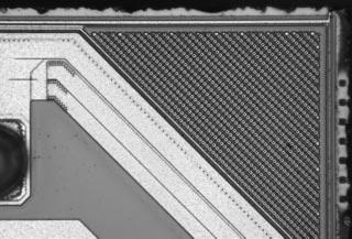
16 PIN 1 Figure 1. Package photographs and x-ray view of the Altera EPM7128SQC Mag. 2.3x.
17 PIN NUMBER FUNCTION PIN NUMBER FUNCTION PIN NUMBER FUNCTION PIN NUMBER FUNCTION V CCIO IO/TDI* GND V CCIO V CCIO GND V CCIO V CCINT GND V CCIO GND /TCK* V CCIO /TDO* GND V CCIO GND INPUTGCLK1 INPUT/EO1 INPUT/GCLRN INPUT/OE2/GCLK2 V CCINT GND *In MAX 7000S devices, this pin may function as either a JTAG port or a user I pin. If the devives is configured to use the JTAG ports for boundary-scan testing or for ISP, this pin is not available as a user pin. Figure 2. Pinout of the Altera EPM7128SQC

18 PIN 88 PIN 113 PIN 80 PIN 121 PIN 160 PIN 1 PIN 41 PIN 33 Figure 3. Whole die photograph of the Altera EPM7128SQC Mag. 24x.


19 Figure 4. Optical views of die corners. Mag. 300x.


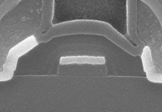
20 METAL 1 METAL 2 PASSIVATION Mag. 3250x METAL 1 METAL 2 PASSIVATION EMBEDDING COMPOUND P+ N+ Mag. 6000x Figure 5. SEM section views illustrating edge seal structure.


21 Mag. 350x Mag. 410x Figure 6. Optical views of die markings.


22 INTERLEVEL DIELECTRIC PASSIVATION METAL 2 METAL 1 SOG LOCAL OXIDE POLYCIDE Mag. 10,000x PASSIVATION METAL 2 PRE-METAL DIELECTRIC INTERLEVEL DIELECTRIC SOG METAL 1 LOCAL OXIDE N+ S/D POLYCIDE GATE Mag. 13,000x Figure 7. SEM section views illustrating general structure.


23 Mag. 5000x Mag. 10,000x Figure 8. SEM views illustrating passivation coverage. 60.


24 PASSIVATION 1 PASSIVATION 2 METAL 2 INTERLEVEL DIELECTRIC Mag. 13,000x TiN CAP PASSIVATION 2 PASSIVATION 1 ALUMINUM 2 INTERLEVEL DIELECTRIC TiW BARRIER Mag. 26,000x Figure 9. SEM section views illustrating metal 2 line profiles.


25 METAL 2 METAL 2 METAL 2 Figure 10. Topological SEM views illustrating metal 2 patterning. Mag. 6500x, 0.


26 METAL 2 Mag. 5000x METAL 2 METAL 1 Mag. 10,000x Figure 11. SEM views illustrating metal 2 step coverage. 60.


27 PASSIVATION TiN CAP METAL 2 TiW BARRIER ILD 2 SOG THINNING METAL 1 ILD 1 TiW BARRIER TiN CAP PASSIVATION INTERLEVEL DIELECTRIC METAL 2 METAL 1 Figure 12. SEM section views illustrating typical metal 2-to-metal 1 vias. Mag. 26,000x. Si METAL 2 BARRIER Figure 13. SEM view illustrating metal 2 barrier. Mag. 20,000x, 45.


28 PASSIVATION METAL 2 SOG METAL 1 POLYCIDE Mag. 13,000x METAL 2 ILD 2 ALUMINUM 1 SOG TiN CAP PRE-METAL DIELECTRIC ILD 1 TiW BARRIER Mag. 26,000x Figure 14. SEM section views illustrating metal 1 line profiles.


29 METAL 1 METAL 1 METAL 1 Figure 15. Topological SEM views illustrating metal 1 patterning. Mag. 6500x, 0.


30 METAL 1 Mag. 5000x METAL 1 Mag. 10,000x Figure 16. SEM views illustrating metal 1 step coverage. 60.


31 INTERLEVEL DIELECTRIC POLISHING ARTIFACT METAL 1 PRE-METAL DIELECTRIC POLYCIDE GATE INTERLEVEL DIELECTRIC TiN CAP THINNING METAL 1 PRE-METAL DIELECTRIC TiW BARRIER Figure 17. SEM section views illustrating typical metal 1 contacts. Glass etch, Mag. 26,000x METAL 1 BARRIER Figure 18. SEM view illustrating metal 1 barrier. Mag. 30,000x, 45.


32 INTERLEVEL DIELECTRIC PRE-METAL DIELECTRIC SOG glass etch METAL 1 POLYCIDE GATE INTERLEVEL DIELECTRIC PRE-METAL DIELECTRIC metal 1-to-N+ METAL 1 LOCAL OXIDE N+ S/D POLYCIDE GATE INTERLEVEL DIELECTRIC METAL 1 PRE-METAL DIELECTRIC metal 1-to-polycide POLYCIDE LOCAL OXIDE Figure 19. Additional SEM section views illustrating metal 1 contacts. Mag. 26,000x.


33 INTERLEVEL DIELECTRIC METAL 1 PRE-METAL DIELECTRIC POLYCIDE LOCAL OXIDE Mag. 26,000x PRE-METAL DIELECTRIC POLYCIDE LOCAL OXIDE Mag. 52,000x Figure 20. SEM section views illustrating polycide profiles.


34 P+ S/D POLYCIDE Mag. 3250x N+ S/D P+ S/D Mag. 6500x POLYCIDE N+ S/D POLYCIDE Mag. 6500x Figure 21. Topological SEM views illustrating polycide patterning. 0.


35 Mag. 4000x POLYCIDE P+ S/D LOCOS Mag. 8000x POLYCIDE N+ S/D POLYCIDE N+ S/D Mag. 16,000x Figure 22. SEM views illustrating polycide step coverage. 60.


36 PRE-METAL DIELECTRIC POLYCIDE GATE P-channel P+ S/D PRE-METAL DIELECTRIC POLYCIDE GATE N-channel N+ S/D PRE-METAL DIELECTRIC POLYCIDE GATE glass etch Figure 23. SEM section views illustrating typical gate structure. Mag. 52,000x.


37 Mag. 1535x P-WELL N-WELL P SUBSTRATE PRE-METAL DIELECTRIC METAL 1 Mag. 26,000x LOCAL OXIDE POLYCIDE STEP AT WELL BOUNDARY PRE-METAL DIELECTRIC POLYCIDE LOCAL OXIDE Mag. 52,000x BIRDSBEAK Figure 24. Section views illustrating well structure and a typical birdsbeak.


38 metal 2 metal 1 polycide Figure 25. SEM views illustrating EEPROM cell array. Mag. 2500x, 60.


39 metal 2 metal 1 polycide TUNNEL OXIDE DEVICE Figure 25a. SEM views illustrating EEPROM cell array. Mag. 5000x, 60.


40 WORD metal 2 ENABLE WORD BIT 1 BIT 2 metal 1 WORD 3 1 GND polycide 2 C TUNNEL OXIDE DEVICE Figure 26. Topological SEM views illustrating EEPROM cell array. Mag. 3250x, 0.


41 WORD metal 2 ENABLE WORD BIT 1 BIT 2 metal 1 Figure 26a. Topological SEM views illustrating EEPROM cell array. Mag. 6500x, 0.

42 AREA OF SECTION GND WORD 3 2 TUNNEL OXIDE DEVICE 1 C polycide WORD BIT 2 BIT 1 3 TUNNEL OXIDE DEVICE 1 2 C ENABLE Figure 26b. Topological SEM view and schematic of EEPROM cell array. Mag. 6500x, 0.


43 WORD BIT 1 TUNNEL OXIDE DEVICE Mag. 6500x BIT 1 Mag. 26,000x Figure 27. SEM section views illustrating EEPROM cell array.


44 TUNNEL OXIDE DEVICE Mag. 26,000x PRE-METAL DIELECTRIC POLYCIDE GATE OXIDE TUNNEL OXIDE glass etch, Mag. 52,000x Figure 27a. SEM section views illustrating the tunnel oxide device in EEPROM circuitry.


45 Mag. 410x Mag. 1000x Figure 28. Optical views illustrating structure and typical circuitry.


46 Au BOND PAD WINDOW M2 M1 Mag. 3250x Au BOND PAD WINDOW M2 M1 POLYCIDE Mag. 5000x Figure 29. SEM section views of bond pad structure.
NKK NR4645LQF Bit RISC Microprocessor
 Construction Analysis NKK NR4645LQF-133 64-Bit RISC Microprocessor Report Number: SCA 9707-547 Global Semiconductor Industry the Serving Since 1964 17350 N. Hartford Drive Scottsdale, AZ 85255 Phone: 602-515-9870
Rockwell R RF to IF Down Converter
 Construction Analysis Rockwell R6732-13 RF to IF Down Converter Report Number: SCA 9709-552 Global Semiconductor Industry the Serving Since 1964 17350 N. Hartford Drive Scottsdale, AZ 85255 Phone: 602-515-9780
Motorola MPA1016FN FPGA
 Construction Analysis Motorola MPA1016FN FPGA Report Number: SCA 9711-561 Global Semiconductor Industry the Serving Since 1964 17350 N. Hartford Drive Scottsdale, AZ 85255 Phone: 602-515-9780 Fax: 602-515-9781
Lattice 3256A-90LM PLD
 Construction Analysis PLD Report Number: SCA 9705-538 Global Semiconductor Industry the Serving Since 1964 17350 N. Hartford Drive Scottsdale, AZ 85255 Phone: 602-515-9780 Fax: 602-515-9781 e-mail: ice@ice-corp.com
Motorola MC68360EM25VC Communication Controller
 Construction Analysis EM25VC Communication Controller Report Number: SCA 9711-562 Global Semiconductor Industry the Serving Since 1964 17350 N. Hartford Drive Scottsdale, AZ 85255 Phone: 602-515-9780 Fax:
Lattice isplsi1032e CPLD
 Construction Analysis Lattice isplsi1032e CPLD Report Number: SCA 9612-522 Global Semiconductor Industry the Serving Since 1964 15022 N. 75th Street Scottsdale, AZ 85260-2476 Phone: 602-998-9780 Fax: 602-948-1925
SGS-Thomson M28C K EEPROM
 Construction Analysis SGS-Thomson M28C64-121 64K EEPROM Report Number: SCA 9710-559 Global Semiconductor Industry the Serving Since 1964 17350 N. Hartford Drive Scottsdale, AZ 85255 Phone: 602-515-9780
Analog Devices ADSP KS-160 SHARC Digital Signal Processor
 Construction Analysis Analog Devices ADSP-21062-KS-160 SHARC Digital Signal Processor Report Number: SCA 9712-575 Global Semiconductor Industry the Serving Since 1964 17350 N. Hartford Drive Scottsdale,
NEC 79VR5000 RISC Microprocessor
 Construction Analysis NEC 79VR5000 RISC Microprocessor Report Number: SCA 9711-567 Global Semiconductor Industry the Serving Since 1964 17350 N. Hartford Drive Scottsdale, AZ 85255 Phone: 602-515-9780
UMC UM F-7 2M-Bit SRAM
 Construction Analysis UMC UM 613264F-7 2M-Bit SRAM Report Number: SCA 9609-511 Global Semiconductor Industry the Serving Since 1964 15022 N. 75th Street Scottsdale, AZ 85260-2476 Phone: 602-998-9780 Fax:
Mosel Vitelic MS62256CLL-70PC 256Kbit SRAM
 Construction Analysis Mosel Vitelic MS62256CLL-70PC 256Kbit SRAM Report Number: SCA 9703-499 Global Semiconductor Industry the Serving Since 1964 17350 N. Hartford Drive Scottsdale, AZ 85255 Phone: 602-515-9780
DEC SA-110S StrongARM 32-Bit Microprocessor
 Construction Analysis DEC SA-110S StrongARM 32-Bit Microprocessor Report Number: SCA 9704-535 Global Semiconductor Industry the Serving Since 1964 15022 N. 75th Street Scottsdale, AZ 85260-2476 Phone:
Maximum MAX662 12V DC-DC Converter
 Construction Analysis Maximum MAX662 12V DC-DC Converter Report Number: SCA 9512-445 Global Semiconductor Industry the Serving Since 1964 17350 N. Hartford Drive Scottsdale, AZ 85255 Phone: 602-515-9780
Oki M A-60J 16Mbit DRAM (EDO)
") Construction Analysis Oki M5117805A-60J 16Mbit DRAM (EDO) Report Number: SCA 9707-545 Global Semiconductor Industry the Serving Since 1964 17350 N. Hartford Drive Scottsdale, AZ 85255 Phone: 602-515-9780
Construction Analysis Oki M5117805A-60J 16Mbit DRAM (EDO) Report Number: SCA 9707-545 Global Semiconductor Industry the Serving Since 1964 17350 N. Hartford Drive Scottsdale, AZ 85255 Phone: 602-515-9780
Micron Semiconductor MT5C64K16A1DJ 64K x 16 SRAM
 Construction Analysis Micron Semiconductor MT5C64K16A1DJ 64K x 16 SRAM Report Number: SCA 9412-394 Global Semiconductor Industry the Serving Since 1964 17350 N. Hartford Drive Scottsdale, AZ 85255 Phone:
Hitachi A 64Mbit (8Mb x 8) Dynamic RAM
 Dynamic RAM") Construction Analysis Hitachi 5165805A 64Mbit (8Mb x 8) Dynamic RAM Report Number: SCA 9712-565 Global Semiconductor Industry the Serving Since 1964 17350 N. Hartford Drive Scottsdale, AZ 85255 Phone:
Construction Analysis Hitachi 5165805A 64Mbit (8Mb x 8) Dynamic RAM Report Number: SCA 9712-565 Global Semiconductor Industry the Serving Since 1964 17350 N. Hartford Drive Scottsdale, AZ 85255 Phone:
Dallas Semicoductor DS80C320 Microcontroller
 Construction Analysis Dallas Semicoductor DS80C320 Microcontroller Report Number: SCA 9702-525 Global Semiconductor Industry the Serving Since 1964 15022 N. 75th Street Scottsdale, AZ 85260-2476 Phone:
Xilinx XC4036XL-1C FPGA
 Construction Analysis Xilinx XC4036XL-1C FPGA Report Number: SCA 9709-553 Global Semiconductor Industry the Serving Since 1964 17350 N. Hartford Drive Scottsdale, AZ 85255 Phone: 602-515-9780 Fax: 602-515-9781
Xilinx XC4036EX FPGA
 Construction Analysis Xilinx XC4036EX FPGA Report Number: SCA 9706-544 Global Semiconductor Industry the Serving Since 1964 15022 N. 75th Street Scottsdale, AZ 85260-2476 Phone: 602-998-9780 Fax: 602-948-1925
SGS-Thomson L4990 Controller
 Construction Analysis SGS-Thomson L4990 Controller Report Number: SCA 9710-560 Global Semiconductor Industry the Serving Since 1964 17350 N. Hartford Drive Scottsdale, AZ 85255 Phone: 602-515-9780 Fax:
Micron Semiconductor MT4LC16M4H9 64Mbit DRAM
 Construction Analysis Micron Semiconductor MT4LC16M4H9 64Mbit DRAM Report Number: SCA 9705-539 Global Semiconductor Industry the Serving Since 1964 15022 N. 75th Street Scottsdale, AZ 85260-2476 Phone:
National Semiconductor LM2672 Simple Switcher Voltage Regulator
 Construction Analysis National Semiconductor LM2672 Simple Switcher Voltage Regulator Report Number: SCA 9712-570 Global Semiconductor Industry the Serving Since 1964 17350 N. Hartford Drive Scottsdale,
Motorola PC603R Microprocessor
 Construction Analysis Motorola PC603R Microprocessor Report Number: SCA 9709-551 Global Semiconductor Industry the Serving Since 1964 17350 N. Hartford Drive Scottsdale, AZ 85255 Phone: 602-515-9780 Fax:
Intel Pentium Processor W/MMX
 Construction Analysis Intel Pentium Processor W/MMX Report Number: SCA 9706-540 Global Semiconductor Industry the Serving Since 1964 15022 N. 75th Street Scottsdale, AZ 85260-2476 Phone: 602-998-9780 Fax:
SGS-Thomson M17C1001 1Mb UVEPROM
 Construction Analysis SGS-Thomson M17C1001 1Mb UVEPROM Report Number: SCA 9612-518 Global Semiconductor Industry the Serving Since 1964 15022 N. 75th Street Scottsdale, AZ 85260-2476 Phone: 602-998-9780
VTC VM365830VSJ Pre-Amp
 Construction Analysis VTC VM365830VSJ Pre-Amp Report Number: SCA 9708-549 Global Semiconductor Industry the Serving Since 1964 17350 N. Hartford Drive Scottsdale, AZ 85255 Phone: 602-515-9780 Fax: 602-515-9781
Integrated Circuit Engineering Corporation. DRAMs
 DRAMs As generally known, the focus of technology in this product category continues to be complex vertical polysilicon structures to reduce cell area. This not only pushes the limits of deposition and
Integrated Circuit Engineering Corporation EPROM
 EPROM There was lots of discussion and many technical papers covering the promises of EPROM (typically Flash) at the IEDM conference last December, but here as in the other memory areas, not much in the
Renesas M5M40R326 32Mbit DRAM Memory Structural Analysis
 August 13, 2004 Renesas M5M40R326 32Mbit DRAM Memory Structural Analysis For questions, comments, or more information about this report, or for any additional technical needs concerning semiconductor technology,
Lecture 030 Integrated Circuit Technology - I (5/8/03) Page 030-1
 Page 030-1") Lecture 030 Integrated Circuit Technology - I (5/8/03) Page 030-1 LECTURE 030 INTEGRATED CIRCUIT TECHNOLOGY - I (References [7,8]) Objective The objective of this presentation is: 1.) Illustrate integrated
Lecture 030 Integrated Circuit Technology - I (5/8/03) Page 030-1 LECTURE 030 INTEGRATED CIRCUIT TECHNOLOGY - I (References [7,8]) Objective The objective of this presentation is: 1.) Illustrate integrated
9/4/2008 GMU, ECE 680 Physical VLSI Design
 ECE680: Physical VLSI Design Chapter II CMOS Manufacturing Process 1 Dual-Well Trench-Isolated CMOS Process gate-oxide TiSi 2 AlCu Tungsten SiO 2 p-well poly n-well SiO 2 n+ p-epi p+ p+ 2 Schematic Layout
Chapter 2 Manufacturing Process
 Digital Integrated Circuits A Design Perspective Chapter 2 Manufacturing Process 1 CMOS Process 2 CMOS Process (n-well) Both NMOS and PMOS must be built in the same silicon material. PMOS in n-well NMOS
Chapter 4 : ULSI Process Integration (0.18 m CMOS Process)
") Chapter : ULSI Process Integration (0.8 m CMOS Process) Reference. Semiconductor Manufacturing Technology : Michael Quirk and Julian Serda (00). - (00). Semiconductor Physics and Devices- Basic Principles(/e)
Chapter : ULSI Process Integration (0.8 m CMOS Process) Reference. Semiconductor Manufacturing Technology : Michael Quirk and Julian Serda (00). - (00). Semiconductor Physics and Devices- Basic Principles(/e)
CMOS Technology. Flow varies with process types & company. Start with substrate selection. N-Well CMOS Twin-Well CMOS STI
 CMOS Technology Flow varies with process types & company N-Well CMOS Twin-Well CMOS STI Start with substrate selection Type: n or p Doping level, resistivity Orientation, 100, or 101, etc Other parameters
ECE321 Electronics I
 ECE321 Electronics I Lecture 19: CMOS Fabrication Payman Zarkesh-Ha Office: ECE Bldg. 230B Office hours: Tuesday 2:00-3:00PM or by appointment E-mail: payman@ece.unm.edu Slide: 1 Miller Effect Interconnect
Manufacturing Process
 CMOS Manufacturing Process CMOS Process 1 A Modern CMOS Process gate-oxide TiSi AlCu Tungsten SiO n+ p-well p-epi poly n-well p+ SiO p+ Dual-Well Trench-Isolated CMOS Process Circuit Under Design V DD
CMOS Manufacturing Process
 CMOS Manufacturing Process CMOS Process A Modern CMOS Process gate-oxide TiSi 2 AlCu Tungsten SiO 2 n+ p-well p-epi poly n-well p+ SiO 2 p+ Dual-Well Trench-Isolated CMOS Process Circuit Under Design V
Manufacturing Process
 Digital Integrated Circuits A Design Perspective Jan M. Rabaey Anantha Chandrakasan Borivoje Nikolic Manufacturing Process July 30, 2002 1 CMOS Process 2 A Modern CMOS Process gate-oxide TiSi 2 AlCu Tungsten
ECE 659. Jan M. Rabaey Anantha Chandrakasan Borivoje Nikolic. July 30, Digital EE141 Integrated Circuits 2nd Manufacturing.
 Digital Integrated Circuits A Design Perspective Jan M. Rabaey Anantha Chandrakasan Borivoje Nikolic Manufacturing Process July 0, 00 1 CMOS Process 1 A Modern CMOS Process gate-oxide TiSi AlCu Tungsten
EE 330 Lecture 9. IC Fabrication Technology Part II. -Oxidation -Epitaxy -Polysilicon -Planarization -Resistance and Capacitance in Interconnects
 EE 330 Lecture 9 IC Fabrication Technology Part II -Oxidation -Epitaxy -Polysilicon -Planarization -Resistance and Capacitance in Interconnects Review from Last Time Etching Dry etch (anisotropic) SiO
ECE520 VLSI Design. Lecture 7: CMOS Manufacturing Process. Payman Zarkesh-Ha
 ECE520 VLSI Design Lecture 7: CMOS Manufacturing Process Payman Zarkesh-Ha Office: ECE Bldg. 230B Office hours: Wednesday 2:00-3:00PM or by appointment E-mail: pzarkesh@unm.edu Slide: 1 Review of Last
EE 560 FABRICATION OF MOS CIRCUITS. Kenneth R. Laker, University of Pennsylvania
 1 EE 560 FABRICATION OF MOS CIRCUITS 2 CMOS CHIP MANUFACTRING STEPS Substrate Wafer Wafer Fabrication (diffusion, oxidation, photomasking, ion implantation, thin film deposition, etc.) Finished Wafer Wafer
Lecture 200 BiCMOS Technology (12/12/01) Page 200-1
 Page 200-1") Lecture 200 BiCMOS Technology (12/12/01) Page 200-1 LECTURE 200 BICMOS TECHNOLOGY (READING: Text-Sec. 2.11) INTRODUCTION Objective Illustrate BiCMOS technology Outline Introduction Physical process illustration
Lecture 200 BiCMOS Technology (12/12/01) Page 200-1 LECTURE 200 BICMOS TECHNOLOGY (READING: Text-Sec. 2.11) INTRODUCTION Objective Illustrate BiCMOS technology Outline Introduction Physical process illustration
Semiconductor Manufacturing Technology. IC Fabrication Process Overview
 Semiconductor Manufacturing Technology Michael Quirk & Julian Serda October 00 by Prentice Hall Chapter 9 IC Fabrication Process Overview /4 Objectives After studying the material in this chapter, you
Microelectronics. Integrated circuits. Introduction to the IC technology M.Rencz 11 September, Expected decrease in line width
 Microelectronics Introduction to the IC technology M.Rencz 11 September, 2002 9/16/02 1/37 Integrated circuits Development is controlled by the roadmaps. Self-fulfilling predictions for the tendencies
Nonplanar Metallization. Planar Metallization. Professor N Cheung, U.C. Berkeley
 Nonplanar Metallization Planar Metallization Passivation Metal 5 (copper) Metal 3 (copper) Interlevel dielectric (ILD) Via (tungsten) Metal 1 (copper) Tungsten Plug to Si Silicon Caps and Plugs oxide oxide
EE BACKEND TECHNOLOGY - Chapter 11. Introduction
 1 EE 212 FALL 1999-00 BACKEND TECHNOLOGY - Chapter 11 Introduction Backend technology: fabrication of interconnects and the dielectrics that electrically and physically separate them. Aluminum N+ Early
CMOS Manufacturing process. Design rule set
 CMOS Manufacturing process Circuit design Set of optical masks Fabrication process Circuit designer Design rule set Process engineer All material: Chap. 2 of J. Rabaey, A. Chandrakasan, B. Nikolic, Digital
Chapter 3 Silicon Device Fabrication Technology
 Chapter 3 Silicon Device Fabrication Technology Over 10 15 transistors (or 100,000 for every person in the world) are manufactured every year. VLSI (Very Large Scale Integration) ULSI (Ultra Large Scale
We are moving to 155 Donner Lab From Thursday, Feb 2 We will be able to accommodate everyone!
 -Spring 006 Digital Integrated Circuits Lecture 4 CMOS Manufacturing Process Design Rules EECS141 1 Good News! We are moving to 155 Donner Lab From Thursday, Feb We will be able to accommodate everyone!
EE 434 Lecture 9. IC Fabrication Technology
 EE 434 Lecture 9 IC Fabrication Technology Quiz 7 The layout of a film resistor with electrodes A and B is shown. If the sheet resistance of the film is 40 /, determine the resistance between nodes A and
Oxidation SMT Yau - 1
 Oxidation Yau - 1 Objectives After studying the material in this chapter, you will be able to: 1. Describe an oxide film for semiconductor manufacturing, including its atomic structure, how it is used
CMOS Processing Technology
 CHAPTER 2 CMOS Processing Technology Outline 2 1. CMOS Technologies 2. Layout Design Rules 3. CMOS Process Enhancements 4. Technology-related CAD Issues 5. Manufacturing Issues CMOS Technologies 3 n-well
CMOS Processing Technology
 CHAPTER 2 CMOS Processing Technology Outline 2 1. CMOS Technologies 2. Layout Design Rules 3. CMOS Process Enhancements 4. Technology-related CAD Issues 5. Manufacturing Issues CMOS Technologies 3 n-well
Silicon Wafer Processing PAKAGING AND TEST
 Silicon Wafer Processing PAKAGING AND TEST Parametrical test using test structures regularly distributed in the wafer Wafer die test marking defective dies dies separation die fixing (not marked as defective)
Manufacturing Process
 Manufacturing Process 1 CMOS Process 2 A Modern CMOS Process gate-oxide TiSi 2 AlCu Tungsten SiO 2 n+ p-well p-epi poly n-well p+ SiO 2 p+ Dual-Well Trench-Isolated CMOS Process 3 Single-crystal ingot
Cost of Integrated Circuits
 Cost of IC Design 1 Cost of Integrated Circuits NRE (Non-Recurrent Engineering) costs fixed design time and effort, mask generation independent of sales volume / number of products one-time cost factor
IC Fabrication Technology Part III Devices in Semiconductor Processes
 EE 330 Lecture 10 IC Fabrication Technology Part III Metalization and Interconnects Parasitic Capacitances Back-end Processes Devices in Semiconductor Processes Resistors Diodes Review from Last Lecture
Fairchild Semiconductor Application Note June 1983 Revised March 2003
 Fairchild Semiconductor Application Note June 1983 Revised March 2003 High-Speed CMOS (MM74HC) Processing The MM74HC logic family achieves its high speed by utilizing microcmos Technology. This is a 3.5
Silicon Epitaxial CVD Want to create very sharp PN boundary grow one type layer on other in single crystal form High dopant layers on low dopant
 Silicon Epitaxial CVD Want to create very sharp PN boundary grow one type layer on other in single crystal form High dopant layers on low dopant substrate Creates latch up protection for CMOS Buried Epi
EE 330 Lecture 9. IC Fabrication Technology Part 2
 EE 330 Lecture 9 IC Fabrication Technology Part 2 Quiz 8 A 2m silicon crystal is cut into wafers using a wire saw. If the wire diameter is 220um and the wafer thickness is 350um, how many wafers will this
Isolation Technology. Dr. Lynn Fuller
 ROCHESTER INSTITUTE OF TECHNOLOGY MICROELECTRONIC ENGINEERING Isolation Technology Dr. Lynn Fuller Motorola Professor 82 Lomb Memorial Drive Rochester, NY 14623-5604 Tel (585) 475-2035 Fax (585) 475-5041
Fabrication and Layout
 Fabrication and Layout Kenneth Yun UC San Diego Adapted from EE271 notes, Stanford University Overview Semiconductor properties How chips are made Design rules for layout Reading Fabrication: W&E 3.1,
CS/ECE 5710/6710. N-type Transistor. N-type from the top. Diffusion Mask. Polysilicon Mask. CMOS Processing
 CS/ECE 5710/6710 CMOS Processing Addison-Wesley N-type Transistor D G +Vgs + Vds S N-type from the top i electrons - Diffusion Mask Mask for just the diffused regions Top view shows patterns that make
Lecture 22: Integrated circuit fabrication
 Lecture 22: Integrated circuit fabrication Contents 1 Introduction 1 2 Layering 4 3 Patterning 7 4 Doping 8 4.1 Thermal diffusion......................... 10 4.2 Ion implantation.........................
Silicon Epitaxial CVD Want to create very sharp PN boundary grow one type layer on other in single crystal form High dopant layers on low dopant
 Silicon Epitaxial CVD Want to create very sharp PN boundary grow one type layer on other in single crystal form High dopant layers on low dopant substrate Creates latch up protection for CMOS Buried Epi
PROCESS FLOW AN INSIGHT INTO CMOS FABRICATION PROCESS
 Contents: VI Sem ECE 06EC63: Analog and Mixed Mode VLSI Design PROCESS FLOW AN INSIGHT INTO CMOS FABRICATION PROCESS 1. Introduction 2. CMOS Fabrication 3. Simplified View of Fabrication Process 3.1 Alternative
Chapter 3 CMOS processing technology
 Chapter 3 CMOS processing technology (How to make a CMOS?) Si + impurity acceptors(p-type) donors (n-type) p-type + n-type => pn junction (I-V) 3.1.1 (Wafer) Wafer = A disk of silicon (0.25 mm - 1 mm thick),
UT Austin, ECE Department VLSI Design 2. CMOS Fabrication, Layout Rules
 2. CMOS Fabrication, Layout, Design Rules Last module: Introduction to the course How a transistor works CMOS transistors This module: CMOS Fabrication Design Rules CMOS Fabrication CMOS transistors are
Semiconductor Manufacturing Technology. Semiconductor Manufacturing Technology
 Semiconductor Manufacturing Technology Michael Quirk & Julian Serda October 2001 by Prentice Hall Chapter 10 Oxidation 2001 2000 by Prentice Hall Diffusion Area of Wafer Fabrication Wafer fabrication (front-end)
10 Manor Parkway, Suite C Salem, New Hampshire
 Micro-Precision Technologies (MPT) is an independent manufacturer of hybrid integrated circuits, multichip modules, and high-precision thick film substrates for the military, medical, avionics, optoelectronics,
1 Thin-film applications to microelectronic technology
 1 Thin-film applications to microelectronic technology 1.1 Introduction Layered thin-film structures are used in microelectronic, opto-electronic, flat panel display, and electronic packaging technologies.
EE CMOS TECHNOLOGY- Chapter 2 in the Text
 1 EE 212 FALL 1999-00 CMOS TECHOLOGY- Chapter 2 in the Text In this set of notes we will describe a modern CMOS process flow. In the simplest CMOS technologies, we need to realize simply MOS and MOS transistors
ECSE 6300 IC Fabrication Laboratory Lecture 8 Metallization. Die Image
 ECSE 6300 IC Fabrication Laboratory Lecture 8 Metallization Prof. Rensselaer Polytechnic Institute Troy, NY 12180 Office: CII-6229 Tel.: (518) 276-2909 e-mails: luj@rpi.edu http://www.ecse.rpi.edu/courses/s18/ecse
TOWARD MEMS!Instructor: Riadh W. Y. Habash
 TOWARD MEMS!Instructor: Riadh W. Y. Habash Students are presented with aspects of general production and manufacturing of integrated circuit (IC) products to enable them to better liaise with and participate
FABRICATION of MOSFETs
 FABRICATION of MOSFETs CMOS fabrication sequence -p-type silicon substrate wafer -creation of n-well regions for pmos transistors, -impurity implantation into the substrate. -thick oxide is grown in the
Czochralski Crystal Growth
 Czochralski Crystal Growth Crystal Pulling Crystal Ingots Shaping and Polishing 300 mm wafer 1 2 Advantage of larger diameter wafers Wafer area larger Chip area larger 3 4 Large-Diameter Wafer Handling
EE 330 Lecture 9. IC Fabrication Technology Part II. -Oxidation -Epitaxy -Polysilicon -Planarization -Resistance and Capacitance in Interconnects
 EE 330 Lecture 9 IC Fabrication Technology Part II -Oxidation -Epitaxy -Polysilicon -Planarization -Resistance and Capacitance in Interconnects Review from Last Time IC Fabrication Technology Crystal Preparation
Chapter 5 Thermal Processes
 Chapter 5 Thermal Processes 1 Topics Introduction Hardware Oxidation Diffusion Annealing Post-Implantation Alloying Reflow High Temp CVD Epi Poly Silicon Nitride RTP RTA RTP Future Trends 2 Definition
Dr. Lynn Fuller Webpage:
 ROCHESTER INSTITUTE OF TECHNOLOGY MICROELECTRONIC ENGINEERING Microelectromechanical Systems (MEMs) Process Integration Dr. Lynn Fuller Webpage: http://people.rit.edu/lffeee 82 Lomb Memorial Drive Rochester,
Cleaning Trends for Advanced Nodes. April 9, 2018 Scotten W. Jones President IC Knowledge LLC
 Cleaning Trends for Advanced Nodes April 9, 2018 Scotten W. Jones President IC Knowledge LLC sjones@icknowledge.com Outline DRAM Logic NAND Conclusion 2 DRAM Nodes 2011 2012 2013 2014 2015 2016 2017 2018
Process Integration. MEMS Release Techniques Sacrificial Layer Removal Substrate Undercut
 Process Integration Self-aligned Techniques LOCOS- self-aligned channel stop Self-aligned Source/Drain Lightly Doped Drain (LDD) Self-aligned silicide (SALICIDE) Self-aligned oxide gap MEMS Release Techniques
Process Integration. NMOS Generic NMOS Process Flow. CMOS - The MOSIS Process Flow
 Process Integration Self-aligned Techniques LOCOS- self-aligned channel stop Self-aligned Source/Drain Lightly Doped Drain (LDD) Self-aligned silicide (SALICIDE) Self-aligned oxide gap MEMS Release Techniques
Semiconductor Manufacturing Technology. Semiconductor Manufacturing Technology
 Semiconductor Manufacturing Technology Michael Quirk & Julian Serda October 2001 by Prentice Hall Chapter 11 Deposition Film Layers for an MSI Era NMOS Transistor Topside Nitride Pre-metal oxide Sidewall
Exam 1 Friday Sept 22
 Exam 1 Friday Sept 22 Students may bring 1 page of notes Next weeks HW assignment due on Wed Sept 20 at beginning of class No 5:00 p.m extension so solutions can be posted Those with special accommodation
Chapter 14. Designing with FineLine BGA Packages
 Chapter 14. Designing with FineLine BGA Packages S53009-1.3 Chapter 14, Designing with FineLine BGA Packages, replaces AN 114: Designing with FineLine BGA Packages. Introduction As programmable logic devices
Qualification and Performance Specification for High Frequency (Microwave) Printed Boards
 Printed Boards") Qualification and Performance Specification for High Frequency (Microwave) Printed Boards Developed by the High Speed/High Frequency Board Performance Subcommittee (D-22) of the High Speed/High Frequency
Qualification and Performance Specification for High Frequency (Microwave) Printed Boards Developed by the High Speed/High Frequency Board Performance Subcommittee (D-22) of the High Speed/High Frequency
Semiconductor Device Fabrication
 5 May 2003 Review Homework 6 Semiconductor Device Fabrication William Shockley, 1945 The network before the internet Bell Labs established a group to develop a semiconductor replacement for the vacuum
VLSI Technology Dr. Nandita Dasgupta Department of Electrical Engineering Indian Institute of Technology, Madras
 VLSI Technology Dr. Nandita Dasgupta Department of Electrical Engineering Indian Institute of Technology, Madras Lecture - 36 MOSFET I Metal gate vs self-aligned poly gate So far, we have discussed about
Mark T. Bohr Intel Senior Fellow, Technology and Manufacturing Group Director, Process Architecture and Integration INTEL CORPORATION
 Mark T. Bohr Intel Senior Fellow, Technology and Manufacturing Group Director, Process Architecture and Integration INTEL CORPORATION Patents» 6762464, N-P butting connections on SOI substrates, 7/13/2004.»
Metallization. Typical current density ~10 5 A/cm 2 Wires introduce parasitic resistance and capacitance
 Metallization Interconnects Typical current density ~10 5 A/cm 2 Wires introduce parasitic resistance and capacitance RC time delay Inter-Metal Dielectric -Prefer low dielectric constant to reduce capacitance
Semiconductor Technology
 Semiconductor Technology von A bis Z Metallization www.halbleiter.org Contents Contents List of Figures List of Tables II III 1 Metallization 1 1.1 Requirements on metallization........................
The History & Future of
 The History & Future of CMP CMPUG July 2008 Karey Holland, Ph.D. kholland@nexplanar.com Ken Cadien, Ph.D. University of Alberta kcadien@ualberta.ca http://www.nexplanar.com http://www.ualberta.ca/ Outline
VLSI Technology Dr. Nandita Dasgupta Department of Electrical Engineering Indian Institute of Technology, Madras
 VLSI Technology Dr. Nandita Dasgupta Department of Electrical Engineering Indian Institute of Technology, Madras Lecture - 33 Problems in LOCOS + Trench Isolation and Selective Epitaxy So, we are discussing
14. Designing with FineLine BGA Packages
 14. Designing with FineLine BGA Packages S51014-1.0 Chapter 14, Designing with FineLine BGA Packages, replaces AN 114: Designing with FineLine BGA Packages. Introduction As programmable logic devices (PLDs)
II. A. Basic Concept of Package.
 Wafer Level Package for Image Sensor Module Won Kyu Jeung, Chang Hyun Lim, Jingli Yuan, Seung Wook Park Samsung Electro-Mechanics Co., LTD 314, Maetan3-Dong, Yeongtong-Gu, Suwon, Gyunggi-Do, Korea 440-743
Review of CMOS Processing Technology
 - Scaling and Integration Moore s Law Unit processes Thin Film Deposition Etching Ion Implantation Photolithography Chemical Mechanical Polishing 1. Thin Film Deposition Layer of materials ranging from
Oxidation Part 1. By Christopher Henderson
 Oxidation Part 1 By Christopher Henderson In this new series, we will discuss the subject of oxidation. Oxidation is a key aspect of the semiconductor process. The fact that one can easily grow an oxide