Green IC packaging: A threath to electronics reliability
|
|
|
- Millicent Davis
- 5 years ago
- Views:
Transcription


1 Green IC packaging: A threath to electronics reliability Geert Willems Steven Thijs, Bart Vandevelde imec 13 juni 2012 Bits & Chips Hardware Conference
2 Content 1. Plastic Molding Compounds 2. Towards Green, low CTE molding compounds 3. The impact of green molding compounds 1. Solder joint fatigue 2. What lifetime is required? 3. What does literature tell us? 4. Failure experience 4. Basics of solder joint fatigue modeling 5. TSOP with GMC 6. BGA with GMC 7. There is more than solder joint reliability Conclusions 2


3 1. Plastic packages: molding compound Plastic molding compounds are used to encapsulate the IC/leadframe or IC/substrate assembly in plastic IC packaging: Leaded packages: SOIC, QFP, TSOP,... Leadless packages: QFN, MLF, LPP,... Area array packages: PBGA 3

 Electrical properties Thermal conductivity Flame retardant")
4 1. Plastic packages: molding compound Molding compound requirements: Compatibility with silicon die & first level interconnect (wire bond, flip chip, die attach) Thermal, mechanical, moisture robustness Leadframe substrate matching (warpage) Electrical properties Thermal conductivity Flame retardant Manufacturability Cost... 4


5 Driven by: 2. Green molding compound Need for reduced moisture sensitivity (lead-free) Going Green trend: Halogen-free plastics Die stress: new IC-dielectrics Cost Greenpeace dashboard Electronic component manufacturers introduced highly SiO 2 filled (85%) Green mold compounds 80% vol 5
6 2. Green molding compounds The change-over took place between (from a leading semiconductor supplier) High penetration level of highly filled GMC All plastic components: SOIC, TSOP, QFN, BGA,... Customer notification is MISLEADING! 2 nd level interconnect reliability has not been considered!? 6
7 3. Impact of Green molding compounds Overmold: CTE 15 ppm/ C 7 ppm/ C Si: 2.6 ppm/ C BT laminate: ~ 14 ppm/ C Printed Circuit Board 17 ppm/ C 1. Better CTE match with silicon lower stress in Si die 2. Higher CTE mismatch with BT laminate more warpage of the package with temperature changes 3. Higher CTE mismatch with PCB higher stress in the solder connections 7


8 3. Impact of Green molding compounds High SiO 2 filling creates molding compound with very low thermal expansion: 6-10 ppm. For reference: CTE Al 2 O 3 = 6.7ppm (ex. CBGA) In the past it matched the PCB CTE of 15-18ppm This creates an upto tenfold increase in thermal mismatch between component and PCB. Depending on component and PCB details: A major increase of thermo-mechanical strain of solder joints and component leads (TSOP). A major threat to solder joint and interconnect reliability 8
 increasing component size (large BGAs, large dies) decreasing stand-off (small ball sizes, leadless packages!")
9 3.1 Solder joint fatigue Thermally induced stress-strain Package L Board S CTEc g CTEb Joint strain ~ g ~ DL/S ~L(CTEc - CTEb)DT/2S Thermo-mechanical strain increases with: increasing thermal mismatch (ceramic, bare silicon, GREEN MOLD COMPOUND ceramic) increasing component size (large BGAs, large dies) decreasing stand-off (small ball sizes, leadless packages!) increasing thermal cycling (outdoor, high power dissipation) 9


10 3.1 Solder joint fatigue Example: 10x10 mm 2 CSP soldered on FR4 PCB after 500 temperature cycles (0 to 100 C) centre SILICON: 2.6 ppm/ºc corner 500 m PCB: : 17 ppm/ºc Micro-crack initation Crack propagation Fracture 10
11 3.1 Solder joint fatigue GMC vs. ceramic CTE GMC (6-10ppm) comparable to ceramic (Al 2 O 3 =6.7ppm) CTE But elasticity of GMC (E-modulus) is an order of magnitude smaller than that of ceramics ten times more flexible. Consequences Package flexibility becomes a dominating factor in the solder joint reliability. The simple Engelmaier approach to solder joint reliability of IPC-D-279, cannot be applied to plastic packages. 11
12 3.2 What is required? Some figures for reference (IPC-9701) 12
13 3.2 What is required? Some figures for reference (IPC-9701) Computer and peripherals: T=20K, 4cpd, 5y, 0.1% N63%(0-100 o C) 1250 cycles/5y Telecom: T=35K, 1cpd, 7-20y, 0.01% N63%(0-100 o C) >2000 cycles/7y cycles/20y Industrial/automotive: T=20K(50%)/40K(27%)/60K(16%)/80K(6%), 365cpy, 10-15y, 0.1% N63%(0-100 o C) >3000 cycles/10y cycles/15y Commercial aircraft: T=20K, 1cpd, 20y, 0.001% N63%(0-100 o C) 3500 cycles/20y Military: T=40K(27%)/60K(73%), 365cpy, 10-20y, 0.1% N63%(0-100 o C) 5500 cycles/10y cycles/20y 10 year lifetime requires Notes: Acc. Factor: SnPb Norris-Landzberg eq. Weibull slope=6 No power cycling Tmax= max. operation N63%(0-100 o C) >3000 cycles (N63%( o C)>1500 cycles) 13
14 3.3 Literature: QFN simulation All simulations confirm reduction in lifetime with a factor 1 to 4. Higher CTE and lower E is recommended: opposite to GMC T.Y. Tee et al., 2003 QFN8x8: -40/150C PCB: 1.6mm 14


15 3.3 Literature: QFN simulation QFN (BLP) -55/125C X. Zhang et al.,
16 3.3 Literature: BGA simulation T.Y. Tee et al., 2006 BGA: -40/125C 16


17 3.3 Literature: experimental QFN QFN7x7: -55/125C PCB: 1.6mm T.Y. Tee et al., 2003 QFN: -40/125C PCB: 1.6mm 17
18 3.3 Literature: experimental BGA (1999) 18


19 3.3 A view from the ceramic packaging world 7 ppm 12 ppm 19

20 3.4. Experimental results (2) Solder joint failure: BGA and TSOP II Lead failure: TSOP I Cu leadframe! 20
21 3. Impact of Green molding compounds Package Type Mean life time with non-green compound (CTE ~ ppm/ C) Mean life time with green compound (CTE ~ 6-8 ppm/ C) Life time reduction introducing green compounds BGA ~ 1100 cycles ~ 500 cycles ~55% QFN 5090 cycles 978 cycles ~80% Most critical components: Large TSOP BGA Partially populated Small pitch QFN TSOP 21


22 4. Basics of solder joint failure modeling Finite Element Model CSP Printed Circuit Board Applied load: temperature cycle (= externally applied or through internal power dissipation) 22

23 4. Basics of solder joint failure modeling start 23

24 4. Basics of solder joint failure modeling start 24
25 4. Basics of solder joint failure modeling Empirical curve for Sn-Ag-Cu solder materials MTTF = N50% = 1464 (e creep in %)
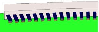
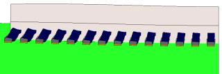
26 5. Reliability of TSOPI & TSOPII TSOP I (56 pins) Package size: ~ 20 X 14 mm 2 TSOP II (54 pins) Cu lead fatigue Solder fatigue


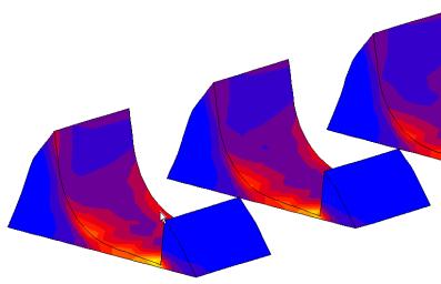
27 5. Reliability of TSOPI TSOP I T min T max Plastic deformation in Cu leads B. Vandevelde, M. Lofrano, G. Willems: Green Mold Compounds: Impact on Second Level Interconnect Reliability EPTC, Singapore, 12/2011
28 5. Reliability of TSOPI Plastic strain per cycle in Cu lead (%) TSOP I CTE overmould (ppm/ C) Bart Vandevelde et al. EPTC 2012
29 5. Reliability of TSOPII TSOP II T min T max Creep strain (-) Bart Vandevelde et al. EPTC 2012
30 MTTF (cycles) 5. Reliability of TSOP with Cu leadframe 85% reduction! TSOP54 95% reduction! TSOP CTE overmould (ppm/ C) (Temperature cycles: 0 to 100 C) Bart Vandevelde et al. EPTC
31 Plastic strain per cycle (%) Plastic strain per cycle (%) 5. Reliability of TSOP with Cu leadframe 6 TSOP54 TSOP TSOP54 TSOP Solder joint Cu lead CTE overmould (ppm/ C) CTE overmould (ppm/ C) Bart Vandevelde - imec 31
32 Plastic strain per cycle (%) Plastic strain per cycle (%) 5. Reliability of TSOP with Alloy42 leadframe 6 TSOP54 TSOP TSOP54 TSOP Solder joint Alloy42 lead CTE overmould (ppm/ C) CTE overmould (ppm/ C) Bart Vandevelde - imec 32


33 6. Reliability of BGA 0.5mm partially populated PBGA FR4 board: 2.1 mm, CTE=17.6 ppm/ C Ball size Ball pitch 0.3 mm 0.5 mm Size 13x13 mm 2 Array size Overmould CTE 24x24 (4 rows 320 balls) 8 ppm/ C 70ºC 10ºC Ramp-time: 15 min Dwell-time: 45 min 33
34 MTTF [x1000 cycles] 6. Reliability of BGA Moulding compound CTE dependency SAC solder joints Divided by 4! Non-Green MC 15 Green MC Overmould CTE [ppm/ C] 34
35 MTTF [x1000 cycles] 6. Reliability of BGA Impact of board thickness Less flexible PCB Board thickness [mm] 35

36 MTTF (cycles) 6. Reliability of BGA Impact of board thickness PBGA 27x27 area array 1.27mm pitch mm 1.6 mm 2.4 mm No PCB flexing EPTC 2012 Bart Vandevelde et al. (0 to 100 C cycling) CTE (ppm/ C) 36

37 6. Reliability of BGA SnPb versus SAC SnPb is significantly worse than lead-free! SnPb SAC Divided by 2 Corner Joint failure β=4 6 8 β=
38 6. Reliability of BGA SnPb versus SAC Why is SnPb version worse than SAC? Stress level dependency (J.-P. Clech) (1) 1.Under low stress conditions lifetime of SAC is higher than that of SnPb. 2.Strain itself depends on the solder alloy. SAC is stronger than SnPb. Therefore SAC solder joints of flexible components on flexible PCBs will deform less than SnPb solder joints under the same conditions of thermal cycling. 38

39 6. Reliability of BGA SAC Stronger connections: more bending of both board and package. Less strain/deformation of solder balls

40 6. Reliability of BGA SnPb Weaker connections: limited board bending because solder balls start to shear (more solder joint deformation)
41 6. Reliability of BGA SnPb versus SAC Why is SnPb version worse than SAC? Stress level dependency (J.-P. Clech) (1) (2) 1.Under low stress conditions lifetime of SAC is higher than that of SnPb. 2.Strain itself depends on the solder alloy. SAC BGA (2) SnPb BGA SAC is stronger than SnPb. Therefore SAC solder joints of flexible components on flexible PCBs will deform less than SnPb solder joints under the same conditions of thermal cycling. 41
42 6. Reliability of BGA No PCB bending No PCB bending yields even more strain SnPb No bending Divided by 6 SnPb bending 42

43 6. Reliability of BGA Increasing strain: no PCB bending Board bending allowed Deformation 50x No board bending allowed PCB stiffners on backside Components on backside BGA back-to-back mounting PCB mounting on backplate/casing Deformation 50x 43


44 6. Reliability of BGA Impact package type Partly populated area array 0.5mm pitch Ball size 0.3mm Fully populated area array 0.8mm pitch Ball size 0.5mm Approximately same ball count and size 44
45 MTTF [x1000] 6. Reliability of BGA Impact package type Changing package type can improve lifetime up to 4x Reliability improves: Higher CTE of molding compound SAC i.s.o. SnPb Larger balls/pitch Fully populated SnPb - No board bending SAC - Board bending allowed mm pitch 4 perimeter rows 0.5 mm pitch 0.8 mm pitch Fully populated 45


46 7. There is more: Head-in-Pillow What: Associated to lead-free soldering? But: Became more and more prevalent 1-2 years after 1/7/2006 Occurs recently also with SnPb soldering. HiP unheard of in SnPb soldering prior to 2008?! 46
47 7. There is more: Head-in-Pillow Major root cause of Head-in-Pillow is component warpage. More warpage when temperature is higher lead-free But: Is now also being reported for SnPb soldering of BGA Seems to have become an issue well after the introduction of leadfree soldering. Lower mold compound CTE will increase/alter the warpage behaviour of PBGA. Look at the GMC introduction Conclusion seems to be: GMC most likely root cause of HiP-epidemic. 50% mid 2007 RoHS 47


48 7. There is more: wire bond fatigue Low cost trends: Green Molding Comp. Reduction in CTE Au Cu wire Increase in CTE Larger CTE mismatch Increased risk of wire bond fatigue! 48
49 8. Conclusions Green, low CTE molding compounds increase the thermal mismatch between plastic packages and the PCB upto tenfold! This creates major issues: Reduction in lifetime below acceptable level due to solder joint failure of plastic packages especially TSOP, BGA, QFN. Complex dependency on package and PCB flexibility. Reduction in lifetime below acceptable level due to Cu lead failure of TSOP type I components. Assembly yield reduction due to Head-in-Pillow of BGA solder joints. Increased risk of Early Failure due to electrically undetected HiP BGA solder joints. Increased risk of wire bond failure. Very limited (and costly) workarounds: underfill (?) 49
50 8. Electronics reliability Green molding compounds constitute a bigger threath to electronics reliability than the switch to lead-free solder ever was! Is SAC more or less (10%...x2) reliable than SnPb vs. increasing solder joint strain upto ten times. Introduced into (qualified!) products without OEM s being aware of it! Especially dangerous for products using SnPb solder, i.e., high reliability products like telecom, automotive, avionics, industrial, safety, medical... 50


51 Dank U voor uw aandacht Vragen? Geert.Willems@imec.be Met steun van het 51
inemi Statement of Work (SOW) inemi Packaging TIG Impact of Low CTE Mold Compound on 2nd Level Solder Joint Reliability Phase 1 & Phase 2
 inemi Packaging TIG Impact of Low CTE Mold Compound on 2nd Level Solder Joint Reliability Phase 1 & Phase 2") inemi Statement of Work (SOW) inemi Packaging TIG Impact of Low CTE Mold Compound on 2nd Level Solder Joint Reliability Phase 1 & Phase 2 Version: 4.1 Date: March 26, 2014 Project Leader: Bart Vandevelde
inemi Statement of Work (SOW) inemi Packaging TIG Impact of Low CTE Mold Compound on 2nd Level Solder Joint Reliability Phase 1 & Phase 2 Version: 4.1 Date: March 26, 2014 Project Leader: Bart Vandevelde
HOW THE MOLD COMPOUND THERMAL EXPANSION OVERRULES THE SOLDER COMPOSITION CHOICE IN BOARD LEVEL RELIABILITY PERFORMANCE
 HOW THE MOLD COMPOUND THERMAL EXPANSION OVERRULES THE SOLDER COMPOSITION CHOICE IN BOARD LEVEL RELIABILITY PERFORMANCE AUTHORS: B. VANDEVELDE, L. DEGRENDELE, M. CAUWE, B. ALLAERT, R. LAUWAERT, G. WILLEMS
Basic Project Information. Background. Version: 2.0 Date: June 29, Project Leader: Bart Vandevelde (imec) inemi Staff: Grace O Malley
 inemi Staff: Grace O Malley") inemi Statement of Work (SOW) Packaging TIG Impact of Low CTE Mold Compound on 2nd Level Solder Joint Reliability Project, Phase 2 (Experimental build and testing) Version: 2.0 Date: June 29, 2015 Project
inemi Statement of Work (SOW) Packaging TIG Impact of Low CTE Mold Compound on 2nd Level Solder Joint Reliability Project, Phase 2 (Experimental build and testing) Version: 2.0 Date: June 29, 2015 Project
Design for Plastic Ball Grid Array Solder Joint Reliability. S.-W. R. Lee, J. H. Lau*
 Page 1 of 9 Design for Plastic Ball Grid Array Solder Joint Reliability The Authors S.-W. R. Lee, J. H. Lau* S.-W. R. Lee, Department of Mechanical Engineering, The Hong Kong University of Science and
Freescale Semiconductor Tape Ball Grid Array (TBGA) Overview
 Overview") Freescale Semiconductor Tape Ball Grid Array (TBGA) Overview Revision 0 2006 Freescale and the Freescale logo are trademarks of Freescale Semiconductor, Inc. All other product or service names are the
Freescale Semiconductor Tape Ball Grid Array (TBGA) Overview Revision 0 2006 Freescale and the Freescale logo are trademarks of Freescale Semiconductor, Inc. All other product or service names are the
Solder joint reliability of cavity-down plastic ball grid array assemblies
 cavity-down plastic ball grid array S.-W. Ricky Lee Department of Mechanical Engineering, The Hong Kong University of Science and, Kowloon, Hong Kong John H. Lau Express Packaging Systems, Inc., Palo Alto,
ELEC 6740 Electronics Manufacturing Chapter 5: Surface Mount Design Considerations
 ELEC 6740 Electronics Manufacturing Chapter 5: Surface Mount Design Considerations R. Wayne Johnson Alumni Professor 334-844 844-1880 johnson@eng.auburn. @eng.auburn.eduedu Outline System Design Issues
ELEC 6740 Electronics Manufacturing Chapter 5: Surface Mount Design Considerations
 ELEC 6740 Electronics Manufacturing Chapter 5: Surface Mount Design Considerations R. Wayne Johnson Alumni Professor 334-844-1880 johnson@eng.auburn. @eng.auburn.eduedu Outline System Design Issues Package
System Level Effects on Solder Joint Reliability
 System Level Effects on Solder Joint Reliability Maxim Serebreni 2004 2010 Outline Thermo-mechanical Fatigue of solder interconnects Shear and tensile effects on Solder Fatigue Effect of Glass Style on
Solder joint reliability of plastic ball grid array with solder bumped flip chip
 ball grid array with solder bumped Shi-Wei Ricky Lee Department of Mechanical Engineering, The Hong Kong University of Science and, Kowloon, Hong Kong John H. Lau Express Packaging Systems, Inc., Palo
Thermo-Mechanical FEM Analysis of Lead Free and Lead Containing Solder for Flip Chip Applications
 Thermo-Mechanical FEM Analysis of Lead Free and Lead Containing Solder for Flip Chip Applications M. Gonzalez 1, B. Vandevelde 1, Jan Vanfleteren 2 and D. Manessis 3 1 IMEC, Kapeldreef 75, 3001, Leuven,
TEMPERATURE CYCLING AND FATIGUE IN ELECTRONICS
 TEMPERATURE CYCLING AND FATIGUE IN ELECTRONICS Gilad Sharon, Ph.D. DfR Solutions Beltsville, MD, USA gsharon@dfrsolutions.com Greg Caswell DfR Solutions Liberty Hill, TX, USA gcaswell@dfrsolutions.com
Reliability of Lead-Free Solder Connections for Area-Array Packages
 Presented at IPC SMEMA Council APEX SM 2001 For additional information, please email marketing@amkor.com Reliability of Lead-Free Solder Connections for Area-Array Packages Ahmer Syed Amkor Technology,
S/C Packaging Assembly Challenges Using Organic Substrate Technology
 S/C Packaging Assembly Challenges Using Organic Substrate Technology Presented by Bernd Appelt ASE Group Nov. 17, 2009 Overview The Packaging Challenge Chip Substrate Interactions Stiffeners for FC-BGA
Effect of Chip Dimension and Substrate Thickness on the Solder Joint Reliability of Plastic Ball Grid Array Packages* S.-W. Lee, J.H.
 Page 1 of 9 Effect of Chip Dimension and Substrate Thickness on the Solder Joint Reliability of Plastic Ball Grid Array Packages* The Authors S.-W. Lee, J.H. Lau** S.-W. Lee, Center for Advanced Engineering
4.10 Exemption no. 8a stakeholder proposal part C (i)
") 4.10 Exemption no. 8a stakeholder proposal part C (i) Lead in high melting temperature solders, i.e. lead based solder alloys containing above 80% by weight of lead 4.10.2 Description of exemption ACEA
4.10 Exemption no. 8a stakeholder proposal part C (i) Lead in high melting temperature solders, i.e. lead based solder alloys containing above 80% by weight of lead 4.10.2 Description of exemption ACEA
Development and Characterization of 300mm Large Panel ewlb (embedded Wafer Level BGA)
") Development and Characterization of 300mm Large Panel ewlb (embedded Wafer Level BGA) Seung Wook Yoon, Yaojian Lin and Pandi C. Marimuthu STATS ChipPAC Ltd. 5 Yishun Street 23, Singapore 768442 E-mail
Development and Characterization of 300mm Large Panel ewlb (embedded Wafer Level BGA) Seung Wook Yoon, Yaojian Lin and Pandi C. Marimuthu STATS ChipPAC Ltd. 5 Yishun Street 23, Singapore 768442 E-mail
Reliability of Interconnects in LED Lighting Assemblies Utilizing Metal Clad Printed Circuit Boards Stefano Sciolè BDM I.M.S.
 Reliability of Interconnects in LED Lighting Assemblies Utilizing Metal Clad Printed Circuit Boards Stefano Sciolè BDM I.M.S. Henkel Electronic Materials Agenda 1. Introduction 2. Motivation 3. Interconnect
Reliability of RoHS-Compliant 2D and 3D 1С Interconnects
 Reliability of RoHS-Compliant 2D and 3D 1С Interconnects John H. Lau, Ph.D. New York Chicago San Francisco Lisbon London Madrid Mexico City Milan New Delhi San Juan Seoul Singapore Sydney Toronto Foreword
Asia/Pacific Semiconductor Packaging and Assembly Facilities, 2002 (Executive Summary) Executive Summary
 Executive Summary") Asia/Pacific Semiconductor Packaging and Assembly Facilities, 2002 (Executive Summary) Executive Summary Publication Date: October 24, 2002 Author Philip Koh This document has been published to the following
Asia/Pacific Semiconductor Packaging and Assembly Facilities, 2002 (Executive Summary) Executive Summary Publication Date: October 24, 2002 Author Philip Koh This document has been published to the following
ACEA/JAMA/KAMA/CLEPA/ et. al. request the exemption of: Lead in high melting temperature solder with lead content > 80%
 No. Criteria 1 Wording of the exemption Materials and components: 1. Lead in high melting temperature solder i.e. lead based solder alloys containing above 80% by weight of lead. Scope and expiry date
Pb-free Challenges for High Complexity Products. inemi Jan 16 th 2008
 Pb-free Challenges for High Complexity Products inemi Jan 16 th 2008 All Rights Reserved Alcatel-Lucent 2007 Agenda RoHS 101 Typical complex of telecom products (different from consumable) Pb-free Concerns
Sherlock 4.0 and Printed Circuit Boards
 Sherlock 4.0 and Printed Circuit Boards DfR Solutions January 22, 2015 Presented by: Dr. Nathan Blattau Senior Vice President 9000 Virginia Manor Rd Ste 290, Beltsville MD 20705 301-474-0607 www.dfrsolutions.com
White Paper Quality and Reliability Challenges for Package on Package. By Craig Hillman and Randy Kong
 White Paper Quality and Reliability Challenges for Package on Package By Craig Hillman and Randy Kong Background Semiconductor technology advances have been fulfilling Moore s law for many decades. However,
5. Packaging Technologies Trends
 5. Packaging Technologies Trends Electronic products and microsystems continue to find new applications in personal, healthcare, home, automotive, environmental and security systems. Advancements in packaging
In this section we take reference to the questionnaire i from OEKO Institute published on May 29 th Abbreviations and Definitions
 9 th Adaptation to scientific and technical progress of Exemptions 8(e), 8(f)(b), 8(g), 8(j) and 14 of Annex II to Directive 2000/53/EC (ELV), Stakeholder Consultation Questionnaire Application for a continuation
Simulation of Embedded Components in PCB Environment and Verification of Board Reliability
 Simulation of Embedded Components in PCB Environment and Verification of Board Reliability J. Stahr, M. Morianz AT&S Leoben, Austria M. Brizoux, A. Grivon, W. Maia Thales Global Services Meudon-la-Forêt,
Board Level Reliability Improvement in ewlb (Embedded Wafer Level BGA) Packages
 Packages") Board Level Reliability Improvement in ewlb (Embedded Wafer Level BGA) Packages by Seng Guan Chow, Yaojian Lin, Bernard Adams * and Seung Wook Yoon** STATS ChipPAC Ltd. 5 Yishun Street 23, Singapore 768442
Board Level Reliability Improvement in ewlb (Embedded Wafer Level BGA) Packages by Seng Guan Chow, Yaojian Lin, Bernard Adams * and Seung Wook Yoon** STATS ChipPAC Ltd. 5 Yishun Street 23, Singapore 768442
Modeling Temperature Cycle Fatigue Life of Select SAC Solders
 Modeling Temperature Cycle Fatigue Life of Select SAC Solders Michael Osterman Center for Advanced Life Cycle Engineering osterman@umd.edu Acknowledgement Special thanks the INEMI Pb-Free Alternative Solder
REDUCTION OF WARPAGE OCCURRENCE STACK-DIE QFN THROUGH FEA AND STATISTICAL METHOD
 REDUCTION OF WARPAGE OCCURRENCE STACK-DIE QFN THROUGH FEA AND STATISTICAL METHOD I. Abdullah, M. Z. M. Talib, I. Ahmad, M. N. B. C. Kamarudin and N. N. Bachok Faculty of Engineering,Universiti Kebangsaan
Parametric Design and Reliability Analysis of Wire Interconnect Technology Wafer Level Packaging
 Y. T. Lin Graduate Assistant C. T. Peng Graduate Assistant K. N. Chiang Associate Professor e-mail: Knchiang@pme.nthu.edu.tw Dept. of Power Mechanical Engineering, National Tsing Hua University, HsinChu
3D-WLCSP Package Technology: Processing and Reliability Characterization
 3D-WLCSP Package Technology: Processing and Reliability Characterization, Paul N. Houston, Brian Lewis, Fei Xie, Ph.D., Zhaozhi Li, Ph.D.* ENGENT Inc. * Auburn University ENGENT, Inc. 2012 1 Outline Packaging
NUMERICAL MODELING OF CYCLIC STRESS-STRAIN BEHAVIOR OF Sn-Pb SOLDER JOINT DURING THERMAL FATIGUE
 NUMERICAL MODELING OF CYCLIC STRESS-STRAIN BEHAVIOR OF Sn-Pb SOLDER JOINT DURING THERMAL FATIGUE M.N. Tamin and Y.B. Liew Department of Applied Mechanics Faculty of Mechanical Engineering 81310 UTM Skudai,
Cost effective 300mm Large Scale ewlb (embedded Wafer Level BGA) Technology
 Technology") Cost effective 300mm Large Scale ewlb (embedded Wafer Level BGA) Technology by Meenakshi Prashant, Seung Wook Yoon, Yaojian LIN and Pandi C. Marimuthu STATS ChipPAC Ltd. 5 Yishun Street 23, Singapore 768442
Cost effective 300mm Large Scale ewlb (embedded Wafer Level BGA) Technology by Meenakshi Prashant, Seung Wook Yoon, Yaojian LIN and Pandi C. Marimuthu STATS ChipPAC Ltd. 5 Yishun Street 23, Singapore 768442
A Solder Joint Reliability Model for the Philips Lumileds LUXEON Rebel LED Carrier Using Physics of Failure Methodology
 A Solder Joint Reliability Model for the Philips Lumileds LUXEON Rebel LED Carrier Using Physics of Failure Methodology Rudi Hechfellner 1, Michiel Kruger 1, Tewe Heemstra 2 Greg Caswell 3, Nathan Blattau
Automotive Electronic Material Challenges. Anitha Sinkfield, Delphi
 Automotive Electronic Material Challenges Anitha Sinkfield, Delphi Automotive Electronic Material Challenges Project Update About inemi Project Participants Problem Statement Project Details Summary and
System-in-Package Research within the IeMRC
 LANCASTER U N I V E R S I T Y Centre for Microsystems Engineering Faculty of Applied Sciences System-in-Package Research within the IeMRC Prof. Andrew Richardson (Lancaster University) Prof. Chris Bailey
Wire-Bond CABGA A New Near Die Size Packaging Innovation Yeonho Choi February 1, 2017
 Amkor Technology, Inc. White Paper Wire-Bond CABGA A New Near Die Size Packaging Innovation Yeonho Choi February 1, 2017 Abstract Expanding its ChipArray Ball Grid Array (CABGA) package form factor miniaturization
ALT of Lead Free CCAs
 ALT of Lead Free CCAs OPS Value Propositions Ops A La Carte is a Professional Reliability Engineering firm focused on providing confidence in reliability. Flexible method of engagement from end to end
Manufacturing and Reliability Challenges With QFN
 Manufacturing and Reliability Challenges With QFN Dr. Craig Hillman and Cheryl Tulkoff DfR Solutions SMTA DC Chapter Ashburn, VA February 25, 2009 QFN as a Next Generation Technology What is Next Generation
Effects of Design, Structure and Material on Thermal-Mechanical Reliability of Large Array Wafer Level Packages
 Effects of Design, Structure and Material on Thermal-Mechanical Reliability of Large Array Wafer Level Packages Bhavesh Varia 1, Xuejun Fan 1, 2, Qiang Han 2 1 Department of Mechanical Engineering Lamar
Packaging Effect on Reliability for Cu/Low k Damascene Structures*
 Packaging Effect on Reliability for Cu/Low k Damascene Structures* Guotao Wang and Paul S. Ho Laboratory of Interconnect & Packaging, TX 78712 * Work supported by SRC through the CAIST Program TRC 2003
Modeling Printed Circuit Boards with Sherlock 3.2
 Modeling Printed Circuit Boards with Sherlock 3.2 DfR Solutions September 23, 2014 Presented by: Dr. Nathan Blattau Senior Vice President 9000 Virginia Manor Rd Ste 290, Beltsville MD 20705 301-474-0607
CSP/BGA BOARD LEVEL RELIABILITY. Abstract
 CSP/BGA BOARD LEVEL RELIABILITY, Reza Ghaffarian, Ph.D. Jet Propulsicm Laboratory California Institute of Technology Pasadena, California (81 8) 354-2059 Abstract Different aspects of advanced surface
Thermal stress analysis of leads in Quad Flat Package: a parametric study
 Thermal stress analysis of leads in Quad Flat Package: a parametric study D. Zhou Faculty of,, zhouding@siswa.um.edu.my A.S.M.A. Haseeb Faculty of, haseeb@um.edu.my A. Andriyana Faculty of, andri.andriyana@um.edu.my
Accurate Predictions of Flip Chip BGA Warpage
 Accurate Predictions of Flip Chip BGA Warpage Yuan Li Altera Corporation 11 Innovation Dr, M/S 422 San Jose, CA 95134 ysli@altera.com, (48)544-758 Abstract Organic flip chip BGA has been quickly adopted
Measurement Note - Crack Detection Methods For Lead-free Solder Joints
 8. References [1] Dusek M, Hunt C, Crack detection methods for lead-free solder joints, April 2004, NPL Report MATC(A)164 [2] Dusek M, Wickham M, Hunt C. The impact of thermal cycle regime on the shear
IMPACT OF LEAD-FREE COMPONENTS AND TECHNOLOGY SCALING FOR HIGH RELIABILITY APPLICATIONS
 IMPACT OF LEAD-FREE COMPONENTS AND TECHNOLOGY SCALING FOR HIGH RELIABILITY APPLICATIONS Chris Bailey, Ph.D. University of Greenwich London, United Kingdom c.bailey@gre.ac.uk ABSTRACT Semiconductor technology
Best Practice Guide for Thermocycling and Reliability Assessment of Solder Joints
 Best Practice Guide for Thermocycling and Reliability Assessment of Solder Joints Miloš Dušek and Christopher Hunt July 2000 July 2000 Best Practice Guide for Thermocycling and Reliability Assessment of
Fundamentals of Sealing and Encapsulation
 Fundamentals of Sealing and Encapsulation Sealing and Encapsulation Encapsulation and sealing are two of the major protecting functions of IC packaging. They are used to protect IC devices from adverse
RELIABILITY OF DOPED LEAD-FREE SOLDER JOINTS UNDER ISOTHERMAL AGING AND THERMAL CYCLING
 As originally published in the SMTA Proceedings RELIABILITY OF DOPED LEAD-FREE SOLDER JOINTS UNDER ISOTHERMAL AGING AND THERMAL CYCLING Cong Zhao, Thomas Sanders, Chaobo Shen, Zhou Hai, John L. Evans,
Design for Flip-Chip and Chip-Size Package Technology
 Design for Flip-Chip and Chip-Size Package Technology Vern Solberg Solberg Technology Consulting Madison, Wisconsin Abstract As new generations of electronic products emerge they often surpass the capability
MARCH National Physical Laboratory Hampton Road Teddington Middlesex United Kingdom TW11 0LW
 NPL REPORT DEPC-MPR 044 Measuring the Impact of Land Size and Solder Joint Volume on Lead-free Solder Joint Reliability M Wickham, L Zou, M Dusek and C P Hunt NOT RESTRICTED MARCH 2006 National Physical
Freescale, the Freescale logo, AltiVec, C-5, CodeTEST, CodeWarrior, ColdFire, C-Ware, t he Energy Efficient Solutions logo, mobilegt, PowerQUICC,
 TM February 2012 Freescale, the Freescale logo, AltiVec, C-5, CodeTEST, CodeWarrior, ColdFire, C-Ware, t he Energy Efficient Solutions logo, mobilegt, PowerQUICC, QorIQ, StarCore and Symphony are trademarks
Adaption to scientific and technical progress under Directive 2002/95/EC
 . Adaption to scientific and technical progress under Directive 2002/95/EC Results previous evaluation Exemption No. 15 Lead in solders to complete a viable electrical connection between semiconductor
!"#$"%&'()#*+,+-&.) )/01)"+.)101) )234)5"#$"%6+%)"7)"889) )!"#$"%6+%):&;-6:&<&+7') )=45&')*>)'6+%8&)#365)5"#$"%&')
#*+,+-&.) )/01)+.)101) )234)5#$%6+%)7)889) )!#$%6+%):&;-6:&<&+7') )=45&')*>)'6+%8&)#365)5#$%&')") !"#$"%&'()#*+,+-&.) )/01)"+.)101) )234)5"#$"%6+%)"7)"889) )!"#$"%6+%):&;-6:&)'6+%8&)#365)5"#$"%&') plastic ceramic DIP DIL PDIP CDIP CerDIP MDIP FDIP SDIP JLCC PLCC CLCC QFP PQFP HQFP RQFP
!"#$"%&'()#*+,+-&.) )/01)"+.)101) )234)5"#$"%6+%)"7)"889) )!"#$"%6+%):&;-6:&)'6+%8&)#365)5"#$"%&') plastic ceramic DIP DIL PDIP CDIP CerDIP MDIP FDIP SDIP JLCC PLCC CLCC QFP PQFP HQFP RQFP
Discrete Capacitor & Resistor Issues. Anthony Primavera Boston Scientific CRM 11/13/06
 Discrete Capacitor & Resistor Issues Anthony Primavera Boston Scientific CRM 11/13/06 Goal: Drive the Industry towards common test methods and best practices in manufacturing to reduce and or eliminate
IPC -7095C Design and Assembly Process Implementation For BGAs
 IPC -7095C Design and Assembly Process Implementation For BGAs 1 Overview With the introduction of BGA components, things had to change: New design New assembly process New repair process New inspection
Adaption to scientific and technical progress under Directive 2002/95/EC
 . Adaption to scientific and technical progress under Directive 2002/95/EC Results previous evaluation Exemption No. 7 a a) Lead in high melting temperature type solders (i.e. lead-based alloys containing
Power Electronics Packaging Solutions for Device Junction Temperature over 220 o C
 EPRC 12 Project Proposal Power Electronics Packaging Solutions for Device Junction Temperature over 220 o C 15 th August 2012 Page 1 Motivation Increased requirements of high power semiconductor device
CHARACTERISATION OF INTERFACIAL CRACKING IN MICROELECTRONIC PACKAGING
 CHARACTERISATION OF INTERFACIAL CRACKING IN MICROELECTRONIC PACKAGING Ian McEnteggart Microelectronics Business Manager Instron Limited, Coronation Road, High Wycombe, Buckinghamshire HP12 3SY www.instron.com/microelectronics
Semiconductor IC Packaging Technology Challenges: The Next Five Years
 SPAY025 May 2006 White Paper Mario A. Bolanos, Director Semiconductor Group Packaging Technology Development, Texas Instruments In the era of communications and entertainment, growth of consumer electronics
Nanium Overview. Company Presentation
 Nanium Overview Company Presentation Nanium Overview Our name and logo nano prefix of Greek origin referring to small objects ium suffix of Latin origin that includes the formation of scientific terms
Reliability Assessment of a High Performance Flip-Chip BGA Package (organic substrate based) using Finite Element Analysis
 using Finite Element Analysis") Reliability Assessment of a High Performance Flip-Chip BGA Package (organic substrate based) using Finite Element Analysis Desmond YR Chong*, R Kapoor, Anthony YS Sun United Test & Assembly Center Ltd
Reliability Assessment of a High Performance Flip-Chip BGA Package (organic substrate based) using Finite Element Analysis Desmond YR Chong*, R Kapoor, Anthony YS Sun United Test & Assembly Center Ltd
Thermo-Mechanical Reliability of Through-Silicon Vias (TSVs)
") 1 Thermo-Mechanical Reliability of Through-Silicon Vias (TSVs) Xi Liu Ph.D. Student and Suresh K. Sitaraman, Ph.D. Professor The George W. Woodruff School of Mechanical Engineering Georgia Institute of
1 Thermo-Mechanical Reliability of Through-Silicon Vias (TSVs) Xi Liu Ph.D. Student and Suresh K. Sitaraman, Ph.D. Professor The George W. Woodruff School of Mechanical Engineering Georgia Institute of
REWORKABLE EDGEBOND APPLIED WAFER-LEVEL CHIP-SCALE PACKAGE (WLCSP) THERMAL CYCLING PERFORMANCE ENHANCEMENT AT ELEVATED TEMPERATURE
 THERMAL CYCLING PERFORMANCE ENHANCEMENT AT ELEVATED TEMPERATURE") REWORKABLE EDGEBOND APPLIED WAFER-LEVEL CHIP-SCALE PACKAGE (WLCSP) THERMAL CYCLING PERFORMANCE ENHANCEMENT AT ELEVATED TEMPERATURE Tae-Kyu Lee, Ph.D. Portland State University Portland, OR, USA taeklee@pdx.edu
REWORKABLE EDGEBOND APPLIED WAFER-LEVEL CHIP-SCALE PACKAGE (WLCSP) THERMAL CYCLING PERFORMANCE ENHANCEMENT AT ELEVATED TEMPERATURE Tae-Kyu Lee, Ph.D. Portland State University Portland, OR, USA taeklee@pdx.edu
INEMI Packaging Substrate Workshop, Toyama, Japan, 2014 Challenges of Organic Substrates from EMS Perspective Weifeng Liu, Ph. D.
 INEMI Packaging Substrate Workshop, Toyama, Japan, 2014 Challenges of Organic Substrates from EMS Perspective Weifeng Liu, Ph. D. Date (4/10/2014) AEG - WW Microelectronics and Packaging OUTLINE Overview
23 rd ASEMEP National Technical Symposium
 THE EFFECT OF GLUE BOND LINE THICKNESS (BLT) AND FILLET HEIGHT ON INTERFACE DELAMINATION Raymund Y. Agustin Janet M. Jucar Jefferson S. Talledo Corporate Packaging & Automation/ Q&R STMicroelectronics,
Assembly Reliability of TSOP/DFN PoP Stack Package
 As originally published in the IPC APEX EXPO Proceedings. Assembly Reliability of TSOP/DFN PoP Stack Package Reza Ghaffarian, Ph.D. Jet Propulsion Laboratory, California Institute of Technology Pasadena,
Qualification of Thin Form Factor PWBs for Handset Assembly
 Qualification of Thin Form Factor PWBs for Handset Assembly Mumtaz Y. Bora Kyocera Wireless Corporation San Diego, Ca. 92121 mbora@kyocera-wreless.com Abstract: The handheld wireless product market place
JOINT INDUSTRY STANDARD
 JOINT INDUSTRY STANDARD AUGUST 1999 Semiconductor Design Standard for Flip Chip Applications ASSOCIATION CONNECTING ELECTRONICS INDUSTRIES Semiconductor Design Standard for Flip Chip Applications About
2ND LEVEL INTERCONNECT RELIABILITY OF CERAMIC AREA ARRAY PACKAGES
 2ND LEVEL INTERCONNECT RELIABILITY OF CERAMIC AREA ARRAY PACKAGES Shingo Sato, Noriyuki Shimizu*, Shin Matsuda, Shoji Uegaki and Sachio Ninomiya Kyocera Corporation Kyoto, Japan Biography Noriyuki Shimizu
Future Electronic Devices Technology in Cosmic Space and Lead-free Solder Joint Reliability
 The 22nd Microelectronics Work Future Electronic Devices Technology in Cosmic Space and Lead-free Solder Joint Reliability Key Points (1) High Speed Solder Ball Shear Test (2) Relationship between Surface
BOARD LEVEL RELIABILITY COMPARISON OF LEAD FREE ALLOYS
 BOARD LEVEL RELIABILITY COMPARISON OF LEAD FREE ALLOYS Robert Darveaux, Corey Reichman, Sabira Enayet, Wen-Sung Hsu, and Win Thandar Swe Amkor Technology, Inc. Chandler, AZ, USA rdarv@amkor.com ABSTRACT
Basic PCB Level Assembly Process Methodology for 3D Package-on-Package
 Basic PCB Level Assembly Process Methodology for 3D Package-on-Package Vern Solberg STC-Madison Madison, Wisconsin USA Abstract The motivation for developing higher density IC packaging continues to be
NEW PRODUCT INTRODUCTION METHODOLOGY FOR RELIABLE SMART PRODUCTS
 NEW PRODUCT INTRODUCTION METHODOLOGY FOR RELIABLE SMART PRODUCTS GEERT WILLEMS IMEC CENTER FOR ELECTRONICS DESIGN & MANUFACTURING Met steun van: CENTER FOR ELECTRONICS DESIGN & MANUFACTURING CEDM IS A
System in Package: Identified Technology Needs from the 2004 inemi Roadmap
 System in Package: Identified Technology Needs from the 2004 inemi Roadmap James Mark Bird Amkor Technology Inc System in package (SiP) technology has grown significantly in the past several years. It
Composition/wt% Bal SA2 (SABI) Bal SA3 (SABI + Cu) Bal
 Bal SA3 (SABI + Cu) Bal") Improving Thermal Cycle and Mechanical Drop Impact Resistance of a Lead-free Tin-Silver-Bismuth-Indium Solder Alloy with Minor Doping of Copper Additive Takehiro Wada 1, Seiji Tsuchiya 1, Shantanu Joshi
Improving Thermal Cycle and Mechanical Drop Impact Resistance of a Lead-free Tin-Silver-Bismuth-Indium Solder Alloy with Minor Doping of Copper Additive Takehiro Wada 1, Seiji Tsuchiya 1, Shantanu Joshi
EFFECT OF Ag COMPOSITION, DWELL TIME AND COOLING RATE ON THE RELIABILITY OF Sn-Ag-Cu SOLDER JOINTS. Mulugeta Abtew
 EFFECT OF Ag COMPOSITION, DWELL TIME AND COOLING RATE ON THE RELIABILITY OF Sn-Ag-Cu SOLDER JOINTS Mulugeta Abtew Typical PCB Assembly Process PCB Loading Solder Paste Application Solder Paste Inspection
A New Creep Constitutive Model for Eutectic Solder Alloy
 X. Q. Shi e-mail: xqshi@gintic.gov.sg Z. P. Wang Gintic Institute of Manufacturing Technology, Nanyang Drive, Singapore 638075 W. Zhou H. L. J. Pang School of Mechanical & Production Engineering, Nanyang
The Shift to Copper Wire Bonding
 The Shift to Copper Wire Bonding E. Jan Vardaman President TechSearch International, Inc. www.techsearchinc.com 1/3/06 3/4/06 5/3/06 7/2/06 8/31/06 10/30/06 12/29/06 2/27/07 4/28/07 6/27/07 8/26/07 10/25/07
Effect of local grain distribution and Enhancement on edgebond applied wafer-level chip-scale package (WLCSP) thermal cycling performance
 thermal cycling performance") Effect of local grain distribution and Enhancement on edgebond applied wafer-level chip-scale package (WLCSP) thermal cycling performance 1 Tae-Kyu Lee, 2 Weidong Xie, 2 Steven Perng, 3 Edward Ibe, and
Effect of local grain distribution and Enhancement on edgebond applied wafer-level chip-scale package (WLCSP) thermal cycling performance 1 Tae-Kyu Lee, 2 Weidong Xie, 2 Steven Perng, 3 Edward Ibe, and
PBA Design-for-Manufacturing Guideline
 PBA Design-for-Manufacturing Guideline EDM-D-001 PCB specification V3.0 July 2017 Contact Verantwoordelijke uitgevers Luc Van den Hove - IMEC Geert Willems Phone: +32 16 288962 Mobile: +32 498 919464 Geert.Willems@imec.be
Designing With High-Density BGA Packages for Altera Devices. Introduction. Overview of BGA Packages
 Designing With High-Density BGA Packages for Altera Devices December 2007, ver. 5.1 Application Note 114 Introduction As programmable logic devices (PLDs) increase in density and I/O pins, the demand for
and Current Reliability Concerns Craig Hillman
 and Pb-Free: Current Reliability Concerns Craig Hillman RoHS Abstract Like the rest of the electronics industry, your products will transition to Removal of Hazardous Substances (RoHS) compliance prior
*EP A2* EP A2 (19) (11) EP A2 (12) EUROPEAN PATENT APPLICATION. (43) Date of publication: Bulletin 2005/08
 (11) EP A2 (12) EUROPEAN PATENT APPLICATION. (43) Date of publication: Bulletin 2005/08") (19) Europäisches Patentamt European Patent Office Office européen des brevets *EP00891A2* (11) EP 1 08 91 A2 (12) EUROPEAN PATENT APPLICATION (43) Date of publication: 23.02.0 Bulletin 0/08 (1) Int Cl.
(19) Europäisches Patentamt European Patent Office Office européen des brevets *EP00891A2* (11) EP 1 08 91 A2 (12) EUROPEAN PATENT APPLICATION (43) Date of publication: 23.02.0 Bulletin 0/08 (1) Int Cl.
THROUGH-SILICON interposer (TSI) is a
 is a") Study on Low Warpage and High Reliability for Large Package Using TSV-Free Interposer Technology Through SMART Codesign Modeling Fa Xing Che, Masaya Kawano, Mian Zhi Ding, Yong Han, and Surya Bhattacharya
Study on Low Warpage and High Reliability for Large Package Using TSV-Free Interposer Technology Through SMART Codesign Modeling Fa Xing Che, Masaya Kawano, Mian Zhi Ding, Yong Han, and Surya Bhattacharya
BOARD LEVEL ASSEMBLY AND RELIABILITY CONSIDERATIONS FOR QFN TYPE PACKAGES
 BOARD LEVEL ASSEMBLY AND RELIABILITY CONSIDERATIONS FOR QFN TYPE PACKAGES Ahmer Syed and WonJoon Kang Amkor Technology, Inc. 1900 S. Price Road Chandler, Arizona ABSTRACT There is a strong interest in
PoP/CSP Warpage Evaluation and Viscoelastic Modeling
 PoP/CSP Warpage Evaluation and Viscoelastic Modeling Wei Lin, Min Woo Lee Amkor Technology 19 S Price Rd, Chandler, AZ 85286 wlin@amkor.com Abstract The purpose of this paper was to evaluate the critical
A.R.E.A. Consortium 2010 Study Plans
 Universal Instruments Advanced Process Laboratory September, 2009 A.R.E.A. Consortium 2010 Study Plans EXECUTIVE SUMMARY The Advanced Research on Electronics Assembly Consortium will continue to fund manufacturing
THERMAL MECHANICAL FATIGUE OF A 56 I/O PLASTIC QUAD-FLAT NOLEAD (PQFN) PACKAGE
 PACKAGE") As originally published in the SMTA Proceedings. THERMAL MECHANICAL FATIGUE OF A 56 I/O PLASTIC QUAD-FLAT NOLEAD (PQFN) PACKAGE Paul Vianco, Ph.D., and Michael K Neilsen, Ph.D. Sandia National Laboratories
As originally published in the SMTA Proceedings. THERMAL MECHANICAL FATIGUE OF A 56 I/O PLASTIC QUAD-FLAT NOLEAD (PQFN) PACKAGE Paul Vianco, Ph.D., and Michael K Neilsen, Ph.D. Sandia National Laboratories
Manufacturing and Reliability Modelling
 Manufacturing and Reliability Modelling Silicon Chip C Bailey University of Greenwich London, England Printed Circuit Board Airflow Temperature Stress at end of Reflow Stress Product Performance in-service
Flip-Chip Underfill: Materials, Process and Reliability
 Flip-Chip Underfill: Materials, Process and Reliability Zhuqing Zhang 1, PhD and C.P. Wong 2, PhD 1 Hewlett-Packard Company, Corvallis, OR 97330 2 School of Materials Science and Engineering & Packaging
ENHANCING MECHANICAL SHOCK PERFORMANCE USING EDGEBOND TECHNOLOGY
 ENHANCING MECHANICAL SHOCK PERFORMANCE USING EDGEBOND TECHNOLOGY Steven Perng, Tae-Kyu Lee, and Cherif Guirguis Cisco Systems, Inc. San Jose, CA, USA sperng@cisco.com Edward S. Ibe Zymet, Inc. East Hanover,
Novel Technique for Flip Chip Packaging of High power Si, SiC and GaN Devices. Nahum Rapoport, Remtec, Inc.
 Novel Technique for Flip Chip Packaging of High power Si, SiC and GaN Devices Nahum Rapoport, Remtec, Inc. 1 Background Electronic Products Designers: under pressure to decrease cost and size Semiconductor
Lifetime Prediction and Design Tool Development for Power Electronics Modules
 Lifetime Prediction and Design Tool Development for Power Electronics Modules Dr Hua Lu and Prof. Chris Bailey University of Greenwich 30 Park Row, London SE0 9 LS IeMRC and Electronics Yorkshire Technical
Failure Modes in Wire bonded and Flip Chip Packages
 Failure Modes in Wire bonded and Flip Chip Packages Mumtaz Y. Bora Peregrine Semiconductor San Diego, Ca. 92121 mbora@psemi.com Abstract The growth of portable and wireless products is driving the miniaturization