Embedded Passives..con0nued
|
|
|
- Rosanna Joseph
- 5 years ago
- Views:
Transcription
1 Embedded Passives..con0nued
2 Why Embedded Passives? Improves the packaging efficiency System-on-Package (SOP); SLIM integration Reducing size Eliminating substrate assembly Minimizing solder joint failure and enhancing reliability Faster and cleaner electrical signals Add functionality More design flexibility? Better reliability? Pb-free Cost savings; near-zero incremental cost?
3 Challenges Resistor tolerance and sheet resistivity: Both resistivity and thickness tolerances are goals which have not been met by resistor materials suitable for resistively required for widespread applications. Yields: Yield loss per device must be extremely small (~ ) because embedded resistors cannot be repaired. Cost: Make new materials and processes cheap enough to reduce the overall cost.


4 Embedded capacitor Types of Embedded capacitor Singulated. Distributed. Types of materials Inorganic Organic

5 Source: ITRI documents
6 Dielectric constant (k) is an intrinsic material property that represents how well a capacitor stores charge when a voltage is applied. Although it is called the dielectric constant, the value changes based on many parameters such as temperature, frequency, voltage and time. As seen in the equation, high dielectric constant results in higher capacitance at a given space. For this reason, higher dielectric constant materials are desired in certain applications where space is limited.


7 CEDT Design Library
8 Embedded capacitor Inorganic methods. Sputtering: chemical vapor deposition (thin film deposition, practiced in micro-electronics industry). Sol-gel: deposition of thin film of materials with higher dielectric constants. (PLZT-Lead Lanthanum Zirconium Titanate ferroelectric*). Anodization: vacuum deposition of aluminum and tantalum to form thin dielectric oxide layer. Ferro electric materials exhibit spontaneous electric dipole moment, high crystal lattice order Para electric materials have crystal phases in which electric poles are unaligned
9 Embedded capacitor Organic methods Polymers: Simple ways of mixing and dispersion. But has low permittivity, otherwise ideal choice. (polyvinylidene fluoride, polyvinylchloride, polypyrrole). Improved safety factor due to suppression of combustion, low ESR Mixed methods Polymer-ceramic: To increase the dielectric constant.
10 A wide range of capacitance from 1pF to many uf is needed for various applications. For filtering and termination relatively low capacitance of 1pF to 200pF is required. For decoupling and energy storage the range is a few nf to a few uf.


11 Steps for fabrication of Embedded Capacitors Figure Source: KJ Lee, Georgia Tech

12 Figure Source: KJ Lee, Georgia Tech Steps for microvia and Cu addition
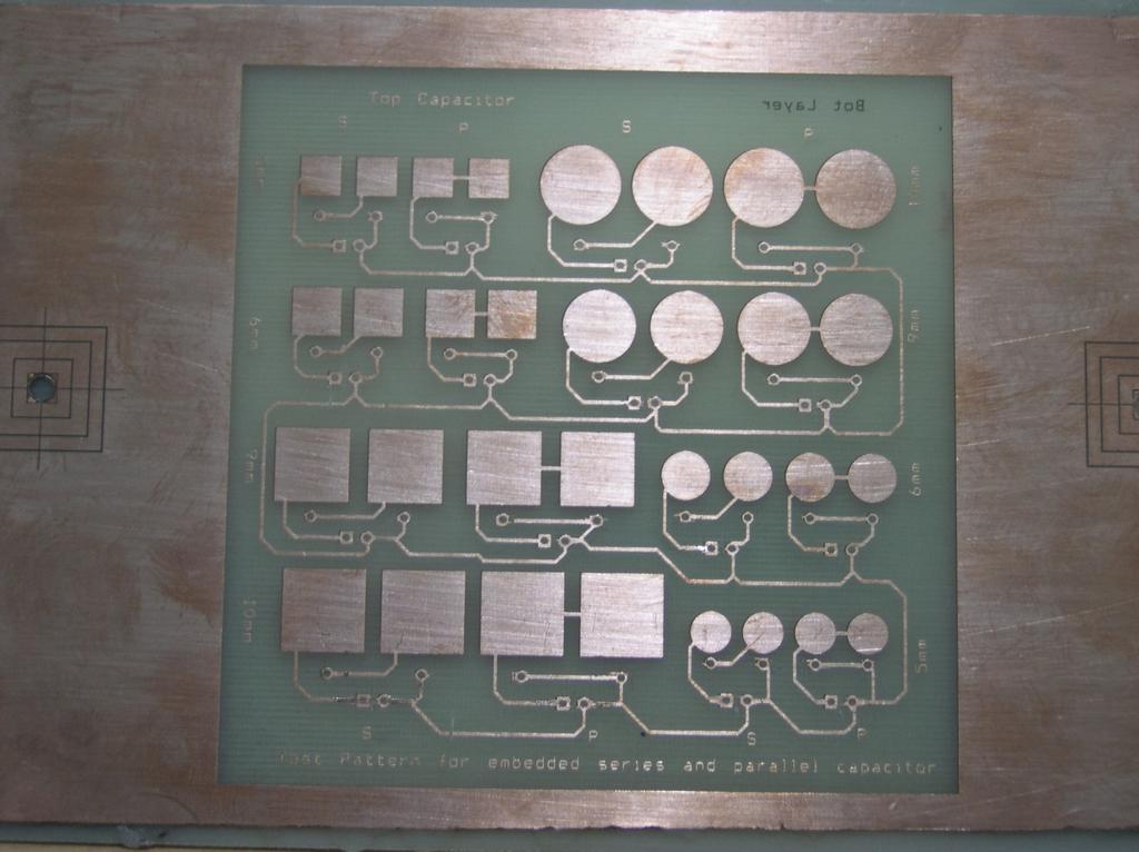
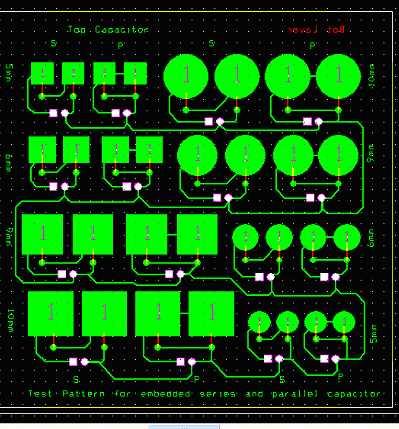
13 CAPACITORS CEDT
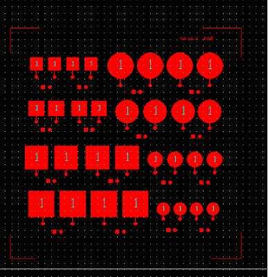
 with embedded R and C Figure")
14 Complete Test vehicle (multi-layer organic substrate) with embedded R and C Figure Courtesy: GTech


15 Characterization Design Reference for R Line Width mm R Foil Ω Design Ref For Cap Product A Product B 24µ 12µ 10 mm mm mm mm mm mm Values of Capacitors obtained in test Board based on area and geometry (pf) Tests and Characterization Adhesion Test: Copper on Dielectric to be checked Dielectric Shrinkage- should be minimal Thermal cycling: 125 C for 100hrs: less than 10% change in R and C values Temp/Humidity cycling: 85 C/85%RH: less than 5% failures Peel Strength: Ni-Cr foil and Ni-P electroless deposits
 Resistance (Ohms) 420 410 400 390 380 370 85 C/85%RH cycling of R foil: 400 hours 1.")
16 900 Thermal Stability of R by electroless method Thermal Reliability and Electrical Test Resistance (Ohms) Duration (Hours) Resistance(Ohms) Thermal stability of R by foil Duration(Hrs.) Resistance (Ohms) C/85%RH cycling of R foil: 400 hours 1.37nF Duration (Hrs) Source: CEDT & Georgia Tech


17 Samples Test board of C foil - first etch Prototype board with microvia Inductor pattern on PWB Fully etched Capacitor patterns Cross-section of a microvia Test board with R and C Resistors by PTF-R material Resistors on Flex Epoxy Base R patterning after inner layer CEDT


18 Ni-P Characterization Assembled Prototypes EDAX of Ni-P from acetate and citrate baths: P content varies from 7-25% Ni-P 25 Bath Ni % P% 20 Acetate Alkaline Citrate Source: CEDT , , , , , , , , , , , , , , , , , , , , , , , , , , , , , , , , , , , , , , 0 XRD analysis shows Ni microcrystalline peak; increase in P content shows lattice disorder of Ni phase SEM photographs of NiCrAlSi from foil, Ni-P from acetate and citrate baths; particle size ~2-3um ~90 resistors embedded
19 CEDT Functional board with embedded R

20 Functional board with embedded C CEDT

21 Prototype board with embedded C and R CEDT
22 Case Study on PWB Miniaturization Implementation Board Type No of layers Component mounting Type Line widths used Via type used Approximate area of board Board area savings Standard Double Sided 2 Through-hole 16, 20, 40 mils TH via 55 mils 75.0 sq. inch Standard Double Sided 2 Mixed type- THT and SMD 12, 16, 20 mils TH via 55 mils 26.8 sq. inch ~60% Multilayer 4 Mixed type- THT and SMD 06, 12, 16 mils Microvia (100um) Buried and TH 16.8 sq. inch ~75% Multilayer (build on both sides) 6 Signal-4 Emb R-2 Mixed type- THT and SMD Emb R ~100 on two sides 06, 12 mils Microvia (100um) Stacked via 12.0 sq. inch ~82% Multilayer (build on only one side) 4 Signal-3 Emb R-1 Mixed type- THT and SMD Emb R~100 on one side 06, 08 mils Microvia (100um) Stacked via 12.0 sq. inch ~82% CEDT work
23 Conclusions Microvia interconnects and Sequential build enables high density packaging at board level. Embedded Passives have been successfully designed by industry and fabricated on multilayered organic substrate. Enables System-on-Package architecture. Resistors can be fabricated by 3 methods: PTF, Foil and Electroless plating Capacitors can be fabricated by foil and polymer-nanocomposite routes. Merges well with conventional PWB fabrication processes and materials. Eliminates through-hole and surface mount components, although SMT is still highly popular. Lead-free assembly enabled with embedded R and C. No standard design library available for embedded components. Laser trim of Resistors will yield better tolerance values. Basic concerns like adhesion, peel strength taken care of. Cost-effective epoxy substrates and interlayer dielectrics used. Less than 10% variation in R, C values after thermal cycling and humidity tests.

24 Figure: Lord Corporation
25 Role of Materials and Processes in Electronics Packaging Diverse and crucial role of materials in packaging Important proper0es of materials relevant to packaging Summary of Processes in packaging
26 Role of materials in Microsystems packaging Figure: Fundamentals of Microsystems Packaging -Rao Tummala
27 Protection Interconnection Heat Dissipation Plastics Epoxy + filters Ceramics Compress Molding Tape casting Dry Pressing Permittivity TCE Thermal conductivity Moisture Absorption Electrical connection Copper Aluminium Gold Thermocomp. Bonding Ultrasonic bonding High I/O density Cu on Polyimide Reliability Environmentally friendly Figure: Fundamentals of Microsystems Packaging -Rao Tummala
28 Figure: Fundamentals of Microsystems Packaging -Rao Tummala
29 Role of Materials in electronics packaging Integrated Circuit Packaging IC Packages IC Assembly System-level packaging Boards Board Assembly
30 Packaging Materials and Processes Electrical Properties Conductivity Permittivity and loss tangent Thermal Properties Thermal conductivity Coefficient of thermal expansion Glass transition temperature
31 Packaging Materials and Processes Mechanical Properties Young s Modulus Chemical Properties Surface tension and wetting Adhesion
32 Thick-film processes Ceramic Screen printing Organic PWB processes Thin-film processes PVD Materials Processing Vacuum evaporation, sputtering CVD Solution based: Physical Spin-coating, meniscus coating, dip coating Solution based: Chemical Sol-gel deposition, Hydrothermal deposition, electroless and electroplating Photolithography
33 Current and future trends in materials and processes Interconnections Organic-based interconnects Non-conductive adhesives Anisotropic conductive adhesives (ACA) Isotropic conductive adhesives (ICA) Low-dielectric constant dielectrics Board materials Underfill materials
Introduction to Embedded Passives
 Introduction to Embedded Passives Passive components PTH, SMD, and now embedded passives Form factor, weight, size, height and OEM capability Tolerance values, material compatibility with PWB processing
Chapter 11: Passives: Discrete, Integrated, and Embedded. Johan Liu
 Chapter 11: Passives: Discrete, Integrated, and Embedded Johan Liu jliu@chalmers.se 1 Types of Passive Components 2 Embedded passive devices: advantages Reduced system mass, volume and footprint. Individual
!"#$#%&#'(() ) **+,-./01)2-,-.3)456,1) /0! **)
 ) **+,-./01)2-,-.3)456,1) /0! **)") !"#$#%&#'(() ) **+,-./01)2-,-.3)456,1) /0!7.5853-09**) B 2 IT is a Toshiba Process Technology 1. Conductive Ag bumps are printed on a sheet of Cu foil. 2. Prepreg is pierced through by the bumps 3. Another
!"#$#%&#'(() ) **+,-./01)2-,-.3)456,1) /0!7.5853-09**) B 2 IT is a Toshiba Process Technology 1. Conductive Ag bumps are printed on a sheet of Cu foil. 2. Prepreg is pierced through by the bumps 3. Another
Embedding Passive and Active Components: PCB Design and Fabrication Process Variations
 Embedding Passive and Active Components: PCB Design and Fabrication Process Variations Vern Solberg Solberg Technical Consulting Saratoga, California USA Abstract Embedding components within the PC board
Chapter 4 Fabrication Process of Silicon Carrier and. Gold-Gold Thermocompression Bonding
 Chapter 4 Fabrication Process of Silicon Carrier and Gold-Gold Thermocompression Bonding 4.1 Introduction As mentioned in chapter 2, the MEMs carrier is designed to integrate the micro-machined inductor
iniaturization of medical devices thanks to flexible substrates ISO 9001 certified
 iniaturization of medical devices thanks to flexible substrates 04-12-2012 Hightec MC Presentation 2 Medical industry is clearly and urgently in need of the development of advanced interconnection solutions
Integration of Power-Supply Capacitors with Ultrahigh Density on Silicon Using Particulate Electrodes POWERSOC 2012
 Integration of Power-Supply Capacitors with Ultrahigh Density on Silicon Using Particulate Electrodes POWERSOC 2012 P M Raj, Himani Sharma, Kanika Sethi, Prof. Rao Tummala 3D Systems Packaging Research
1.3.2 Nanotechnology Nanoporosity Deposition Methods Dissolution Methods
 Table of Contents 1. Metal Finishing 1 1.1 Introduction 1 1.1.1 Description of Industrial Activity Covered 1 1.1.2 Environmental and Legislative Background 3 1.1.3 Emerging Technology or Research? 4 1.2
Anisotropic Conductive Films (ACFs)
") Anisotropic Conductive Films (ACFs) ACF = Thermosetting epoxy resin film + Conductive particles Chip or substrate 1 Heat Pressure ACF Substrate 2 Chip or substrate 1 ACF Substrate 2 Applications Chip-on-Board
Anisotropic Conductive Films (ACFs) ACF = Thermosetting epoxy resin film + Conductive particles Chip or substrate 1 Heat Pressure ACF Substrate 2 Chip or substrate 1 ACF Substrate 2 Applications Chip-on-Board
Manufacturing Technologies for MEMS and SMART SENSORS
 4 Manufacturing Technologies for MEMS and SMART SENSORS Dr. H. K. Verma Distinguished Professor (EEE) Sharda University, Greater Noida (Formerly: Deputy Director and Professor of Instrumentation Indian
Building HDI Structures using Thin Films and Low Temperature Sintering Paste
 Building HDI Structures using Thin Films and Low Temperature Sintering Paste Catherine Shearer, James Haley and Chris Hunrath Ormet Circuits Inc. - Integral Technology California, USA chunrath@integral-hdi.com
LTCC SYSTEMS and LTCC DESIGN RULES
 LTCC SYSTEMS and LTCC DESIGN RULES Low Temperature Co-fired Ceramic revision status: G page 1 of 19 Table of Contents: 1 General page 3 2 Commercial LTCC tape systems page 4 3 Design possibilities page
Flexible Substrates for Smart Sensor Applications
 Flexible Substrates for Smart Sensor Applications A novel approach that delivers miniaturized, hermetic, biostable and highly reliable smart sensor modules. AUTHORS Dr. Eckardt Bihler, Dr. Marc Hauer,
General Introduction to Microstructure Technology p. 1 What is Microstructure Technology? p. 1 From Microstructure Technology to Microsystems
 General Introduction to Microstructure Technology p. 1 What is Microstructure Technology? p. 1 From Microstructure Technology to Microsystems Technology p. 9 The Parallels to Microelectronics p. 15 The
Introducing KEMET Tantalum Low DC Leakage MnO2 Series. One WORLD One Brand One Strategy One Focus One Team One KEMET
 Introducing KEMET Tantalum Low DC Leakage MnO2 Series One WORLD One Brand One Strategy One Focus One Team One KEMET Purpose Introduce KEMET s Low DC Leakage MnO2 Series () Objectives Define the features
Qualification and Performance Specification for High Frequency (Microwave) Printed Boards
 Printed Boards") Qualification and Performance Specification for High Frequency (Microwave) Printed Boards Developed by the High Speed/High Frequency Board Performance Subcommittee (D-22) of the High Speed/High Frequency
Qualification and Performance Specification for High Frequency (Microwave) Printed Boards Developed by the High Speed/High Frequency Board Performance Subcommittee (D-22) of the High Speed/High Frequency
Metallization deposition and etching. Material mainly taken from Campbell, UCCS
 Metallization deposition and etching Material mainly taken from Campbell, UCCS Application Metallization is back-end processing Metals used are aluminum and copper Mainly involves deposition and etching,
Welcome to Streamline Circuits Lunch & Learn. Design for Reliability & Cost Reduction of Advanced Rigid-Flex/Flex PCB Technology
 Welcome to Streamline Circuits Lunch & Learn Design for Reliability & Cost Reduction of Advanced Rigid-Flex/Flex PCB Technology Accurate PCB data is critical to the tooling process. Here are some key items
Low Impedance Ta Capacitors to Serve the Needs of the Electronics Industry
 Low Impedance Ta Capacitors to Serve the Needs of the Electronics Industry Randy Hahn, and Jonathan Paulsen KEMET Electronics Corp PO Box 5928 Greenville, SC 29606 Tel: +1 864-963-6300 Fax: +1 864-228-4333
CLAD MATERIAL ~ FINE CLAD is a solution for high density, low cost PWB.
 ~ CLAD MATERIAL ~ FINE CLAD is a solution for high density, low cost PWB. Principle of bonding technique Principle of bonding technique Step 1 Material A, B In vacuum Step 2 Surface activated treatment
Cu electroplating in advanced packaging
 Cu electroplating in advanced packaging March 12 2019 Richard Hollman PhD Principal Process Engineer Internal Use Only Advancements in package technology The role of electroplating Examples: 4 challenging
Polymer Nanocomposites, Printable and Flexible Technology for Electronic Packaging
 Polymer Nanocomposites, Printable and Flexible Technology for Electronic Packaging Rabindra N. Das, Frank D. Egitto, Bill Wilson, Mark D. Poliks, and Voya R. Markovich Endicott Interconnect Technologies,
1/2W, 0805 Low Resistance Chip Resistor (Lead / Halogen free)
") 1. Scope 1/2W, 0805 (Lead / Halogen free) This specification applies to 1.2mm x 2.0mm size 1/2W, fixed metal film chip resistors rectangular type for use in electronic equipment. 2. Type Designation RL
1. Scope 1/2W, 0805 (Lead / Halogen free) This specification applies to 1.2mm x 2.0mm size 1/2W, fixed metal film chip resistors rectangular type for use in electronic equipment. 2. Type Designation RL
ALTIUMLIVE 2018: NAVIGATING THE COMPLEXITIES OF PCB MATERIAL SELECTION
 ALTIUMLIVE 2018: NAVIGATING THE COMPLEXITIES OF PCB MATERIAL SELECTION Chris Hunrath Insulectro, VP of Technology San Diego October 4 Outline 1 PCB Material Overview 2 What is the Dielectric Constant of
Description. Spectro Tabs, higher purity conductive carbon tabs,12mm O.D.
 Description SPEC The simplicity of application and smooth, clean surfaces of PELCO Tabs Carbon Conductive Tabs are a significant improvement compared to many of the other common adhesives that have been
Fine Pitch P4 Probe Cards
 Fine Pitch P4 Probe Cards Photolithographic Pattern Plating Process June 1998 By Toshi Ishii, Hide Yoshida Contents What is a P4 probe card? Specification Some test results Tip cleaning RF performance
METHODS OF COATING FABRICATION
 METHODS OF COATING FABRICATION Zbigniew Grzesik http://home.agh.edu.pl/~grzesik Department of Physical Chemistry and Modelling DEFINITION The coating is the thin outer layer of the object, which physiochemical
Interconnects. Outline. Interconnect scaling issues Aluminum technology Copper technology. Properties of Interconnect Materials
 Interconnects Outline Interconnect scaling issues Aluminum technology Copper technology 1 Properties of Interconnect Materials Metals Silicides Barriers Material Thin film Melting resistivity point ( C)
Facedown Termination for Higher C/V - Lower ESL Conductive-Polymer SMT Capacitors
 Facedown Termination for Higher C/V - Lower ESL Conductive-Polymer SMT Capacitors Edward Chen 1, Ken Lai 2, John Prymak 3, Mike Prevallet 3 KEMET Electronics Corp. Taiwan Branch, 3-4F, No. 148, Section
MEPTEC Semiconductor Packaging Technology Symposium
 MEPTEC Semiconductor Packaging Technology Symposium Advanced Packaging s Interconnect Technology Process Shift and Direction October 23, 2014 Jay Hayes- Director of Business Development -Bumping and Flip
2003 Ceramic Interconnect Technology Conference. Performance of Low-Ohmic Co-Fired Buried Resistors in A6S Tape
 23 Ceramic Interconnect Technology Conference Performance of Low-Ohmic Co-Fired Resistors in A6S Tape Michail Moroz Ferro Electronic Material Systems 1395 Aspen Way Vista, CA 9283 E-mail: morozm@ferro.com
MACDERMID ENTHONE ELECTRONICS SOLUTIONS BLACKHOLE/ECLIPSE
 MACDERMID ENTHONE ELECTRONICS SOLUTIONS BLACKHOLE/ECLIPSE DEC, 2016 OUTLINE Mechanism of Blackhole / Eclipse Blackhole / Eclipse process - Sequence - Process Equipment enhancement Performance test method
EE 5344 Introduction to MEMS. CHAPTER 3 Conventional Si Processing
 3. Conventional licon Processing Micromachining, Microfabrication. EE 5344 Introduction to MEMS CHAPTER 3 Conventional Processing Why silicon? Abundant, cheap, easy to process. licon planar Integrated
Low Temperature Co-fired Ceramics (LTCC) Multi-layer Module Boards
 Multi-layer Module Boards") Low Temperature Co-fired Ceramics () Multi-layer Module Boards Example: Automotive Application Example: Communication Application Murata's Low Temperature Co-fired Ceramics offer highly integrated substrates
Low Temperature Co-fired Ceramics () Multi-layer Module Boards Example: Automotive Application Example: Communication Application Murata's Low Temperature Co-fired Ceramics offer highly integrated substrates
Electrical and Fluidic Microbumps and Interconnects for 3D-IC and Silicon Interposer
 Electrical and Fluidic Microbumps and Interconnects for 3D-IC and Silicon Interposer Li Zheng, Student Member, IEEE, and Muhannad S. Bakir, Senior Member, IEEE Georgia Institute of Technology Atlanta,
CX Thin Fil s. Resistors Attenuators Thin-Film Products Thin-Film Services. ISO 9001:2008 RoHS/REACH Compliant ITAR Compliant
 CX Thin Fil s Resistors Attenuators Thin-Film Products Thin-Film Services www.cxthinfilms.com ISO 9001:2008 RoHS/REACH Compliant ITAR Compliant www.cxthinfilms.com sales@cxthinfilms.com +1 (401) 461-5500
10 Manor Parkway, Suite C Salem, New Hampshire
 Micro-Precision Technologies (MPT) is an independent manufacturer of hybrid integrated circuits, multichip modules, and high-precision thick film substrates for the military, medical, avionics, optoelectronics,
2W, 2512, 4-Terminal, Low Resistance Chip Resistor (Lead / Halogen Free)
") 2W, 2512, 4-Terminal, Low Resistance Chip Resistor (Lead / Halogen Free) 1. Scope This specification applies to 3.2mm x 6.4mm size 2W, fixed metal foil with ceramic carrier current sensing resistors used
2W, 2512, 4-Terminal, Low Resistance Chip Resistor (Lead / Halogen Free) 1. Scope This specification applies to 3.2mm x 6.4mm size 2W, fixed metal foil with ceramic carrier current sensing resistors used
Application Guide, SPA Capacitors
 Tape Specifications Application Guide, SPA Solid Polymer Aluminum Reel Specifications mm SPA Type ESRL ESRD (.8 mm Ht.) ESRD (3. mm Ht.) ESRE W ±.3 t 2.4 ±. 2 2. ±. 2 3.4 ±. 2 4.5 ±. 2 E F D + /-. Pø P
Opti - Cap March 2011 P42BN820MA3152
 Opti - Cap March 2011 P42BN820MA3152 MAXIMUM ENVELOPE (SEE TABLE) Multilayer Capacitor.040 ±.002 Milli Cap.005 ±.001.038 ±.004 Termination Metallization: 7.5 ± 4.5 microinches Au over a minimum of 50 microinches
12 Technical Paper. Key words: PPR electroplating, via fill, thermal management, through hole fill
 12 Technical Paper The Effects of Board Design on Electroplated Copper Filled Thermal Vias for Heat Management Carmichael Gugliotti, Rich Bellemare MacDermid Enthone Electronics Solutions Waterbury, CT,
The Effects of Board Design on Electroplated Copper Filled Thermal Vias for Heat Management
 The Effects of Board Design on Electroplated Copper Filled Thermal Vias for Heat Management Carmichael Gugliotti, Rich Bellemare MacDermid Enthone Electronics Solutions Waterbury, CT, USA Richard.bellemare@macdermidenthone.com
Qualification and Performance Specification for Flexible Printed Boards
 Qualification and Performance Specification for Flexible Printed Boards Developed by the Flexible Circuits Performance Specifications Subcommittee (D-12) of the Flexible Circuits Committee (D-10) of IPC
High Temperature Ta/MnO 2 Capacitors
 High Temperature Ta/MnO 2 Capacitors Y. Freeman, A. Chacko, P. Lessner, S. Hussey, R. Marques, and J. Moncada KEMET Electronics Corporation, 2835 KEMET Way, Simpsonville, SC 29681, yurifreeman@kemet.com
Cost Effective 3D Glass Microfabrication for Advanced Packaging Applications
 Cost Effective 3D Glass Microfabrication for Advanced Packaging Applications Authors: Jeb. H Flemming, Kevin Dunn, James Gouker, Carrie Schmidt, Roger Cook ABSTRACT Historically, while glasses have many
DATA SHEET SURFACE-MOUNT CERAMIC MULTILAYER CAPACITORS Low-Inductance X5R / X7R
 Product Specification November 21, 2016 V.1 DATA SHEET SURFACE-MOUNT CERAMIC MULTILAYER CAPACITORS - X5R / X7R 6.3 V TO 50 V 10 nf to 1 uf RoHS compliant & Halogen Free 2 SCOPE This specification describes
Surface Micromachining
 Surface Micromachining Outline Introduction Material often used in surface micromachining Material selection criteria in surface micromachining Case study: Fabrication of electrostatic motor Major issues
Embedding of Active Components in LCP for Implantable Medical Devices
 44 th IMAPS New England Symposium 2017 Embedding of Active Components in LCP for Implantable Medical Devices Dr. Eckardt Bihler and Dr. Marc Hauer, Dyconex AG Susan Bagen, PE, Micro Systems Technologies,
Sn-Pb plating or Tin plating
 2/14 Unit mm L a a Code letter Dimension L 2..2 W 1.25.2 W t a b.4.1.4.2.4.2 t b b Fig.1 Construction and dimensions NOTE : Resistive element Electrode Protective coat Substrate Nichrome alloy thin film
Lamination-Based Technology For High Performance Metallic Magnetic Cores
 Lamination-Based Technology For High Performance Metallic Magnetic Cores Florian Herrault and Mark G. Allen School of Electrical and Computer Engineering Georgia Institute of Technology Atlanta, GA 30332-0250
Editorial Manager(tm) for Microsystem Technologies Manuscript Draft
 for Microsystem Technologies Manuscript Draft") Editorial Manager(tm) for Microsystem Technologies Manuscript Draft Manuscript Number: Title: Electrical and Reliability Properties of Isotropic Conductive Adhesives on Immersion Silver Printed-Circuit
Editorial Manager(tm) for Microsystem Technologies Manuscript Draft Manuscript Number: Title: Electrical and Reliability Properties of Isotropic Conductive Adhesives on Immersion Silver Printed-Circuit
Preface Preface to First Edition
 Contents Foreword Preface Preface to First Edition xiii xv xix CHAPTER 1 MEMS: A Technology from Lilliput 1 The Promise of Technology 1 What Are MEMS or MST? 2 What Is Micromachining? 3 Applications and
GRAPHIC MANUFACTURING CAPABILITY Q217-18
 All features are design dependent and may not be achievable in combination Reduced Yield / Special values up ( or down ) to the standard limit are design and application dependent Standard features only
Solid State Sensors. Microfabrication 8/22/08 and 8/25/08
 Solid State Sensors Microfabrication 8/22/08 and 8/25/08 Purpose of This Material To introduce the student to microfabrication techniques as used to fabricate MEMS Sensors Understand concepts not specifics
Cal-Chip Electronics, Incorporated Thick Film Chip Resistors - RM Series
 Thick Film Chip Resistors - RM Series Fixed Chip Resistors manufactured for more compact electronic components and automatic mounting system. These Chip Resistors have electrical stability and mechanical
PARYLENE ENGINEERING. For Longer Lasting Products
 PARYLENE ENGINEERING For Longer Lasting Products PARYLENE ENGINEERING This presentation serves as a quick overview of the conformal coating material and processes currently used in the industry. The field
All-Polyimide Thermal Interface Products
 All-Polyimide Thermal Interface Products SMTA Harsh Environment Electronics Workshop Dearborn, MI 6/24/03 Jim Fraivillig Fraivillig Technologies Boston, MA Why polyimide? HARSH ENVIRONMENT ELECTRONICS.
Metallization of MID Dec 2 010
 Metallization of MID Dec 2010 Agenda Introduction to Dow Electronic Materials MID Applications & Advantages Dow MID Metallization Processes Plating Equipment Summary Dow Business Structure Where Dow Electronic
Relative Reliability Measurements for Electrically Conductive Adhesive Joints on Subtractive Thermoplastic Substrates
 Relative Reliability Measurements for Electrically Conductive Adhesive Joints on Subtractive Thermoplastic Substrates Summary This Note describes a new combinational test method for the measurement of
Figure 1 Embedded Active and Passive Module (EMAP) Cross-section Schematic
 Cross-section Schematic") Super High Density Two Metal Layer Ultra-Thin Organic Substrates for Next Generation System-On-Package (SOP), SIP and Ultra-Fine Pitch Flip-Chip Packages Venky Sundaram, Hunter Chan, Fuhan Liu, and Rao
Super High Density Two Metal Layer Ultra-Thin Organic Substrates for Next Generation System-On-Package (SOP), SIP and Ultra-Fine Pitch Flip-Chip Packages Venky Sundaram, Hunter Chan, Fuhan Liu, and Rao
Introduction of CSC Pastes
 Introduction of CSC Pastes Smart Phones & Conductive Pastes Chip Varistors Chip Inductors LC Filters Flexible Printed Circuit Boards Electronic Molding Compounds ITO Electrodes PCB Through Holes Semiconductor
Introduction Conductors. Supply Planes. Dielectric. Vias PCB Manufacturing Process Electronic Assembly Manufacturing Process
 PCBs/Overview Printed Circuit Boards (PCB) Introduction Conductors. Supply Planes. Dielectric. Vias PCB Manufacturing Process Electronic Assembly Manufacturing Process 29/09/2005 EE6471 (KR) 263 PCBs/Overview
Surface Micromachining of Uncooled Infrared Imaging Array Using Anisotropic Conductive Film
 Surface Micromachining of Uncooled Infrared Imaging Array Using Anisotropic Conductive Film Weiguo Liu, Lingling Sun, Weiguang Zhu, Ooi Kiang Tan Microelectronics Center, School of Electrical and Electronic
Passive component embedding in printed circuit boards for space applications
 Passive component embedding in printed circuit boards for space applications 2nd Space Passive Component Days (SPCD), International Symposium 12-14 October 2016 ESA/ESTEC, Noordwijk, The Netherlands Maarten
By Ron Blankenhorn, Pac Tech USA, Santa Clara, Calif., and Thomas Oppert, Pac Tech GbmH, Nauen, Germany
 INTRODUCTION Modern microelectronic products require packages that address the driving forces of reduced size and weight, as well as increased performance at high frequencies. Flipchip and direct chip
Application Note. Capacitor Selection for Switch Mode Power Supply Applications
 Application Note AN37-0013 Capacitor Selection for Switch Mode Power Supply Applications 1. Introduction Faced with the availability of multiple capacitor options for use in high reliability SMPS applications,
Polymer Tantalum Capacitors for Automotive Applications
 CARTS International 2014 March 31-April 3, 2014 Introduction Polymer Tantalum Capacitors for Automotive Applications Jayson Young and Javaid Qazi Kemet Corporation PO Box 5928, Greenville SC 29606 Phone:
CMOS Technology. Flow varies with process types & company. Start with substrate selection. N-Well CMOS Twin-Well CMOS STI
 CMOS Technology Flow varies with process types & company N-Well CMOS Twin-Well CMOS STI Start with substrate selection Type: n or p Doping level, resistivity Orientation, 100, or 101, etc Other parameters
A new Glass GEM with a single sided guard-ring structure
 A new Glass GEM with a single sided guard-ring structure RD-51 session! 5 July, 2013!! Yuki MITSUYA a, Takeshi FUJIWARA b, Hiroyuki TAKAHASHI a!! a Department of Nuclear Engineering and Management, The
High Stability Resistor Chips (< 0.25 % at Pn at 70 C during 1000 h) Thick Film Technology
 Thick Film Technology") High Stability Resistor Chips (< 0.25 % at Pn at 70 C during 0 h) Thick Film Technology thick film resistor chips are specially designed to meet very stringent specifications in terms of reliability, stability
High Stability Resistor Chips (< 0.25 % at Pn at 70 C during 0 h) Thick Film Technology thick film resistor chips are specially designed to meet very stringent specifications in terms of reliability, stability
EP A2 (19) (11) EP A2 (12) EUROPEAN PATENT APPLICATION. (43) Date of publication: Bulletin 2006/23
 (11) EP A2 (12) EUROPEAN PATENT APPLICATION. (43) Date of publication: Bulletin 2006/23") (19) Europäisches Patentamt European Patent Office Office européen des brevets (12) EUROPEAN PATENT APPLICATION (11) EP 1 667 226 A2 (43) Date of publication: 07.06.06 Bulletin 06/23 (1) Int Cl.: H01L
(19) Europäisches Patentamt European Patent Office Office européen des brevets (12) EUROPEAN PATENT APPLICATION (11) EP 1 667 226 A2 (43) Date of publication: 07.06.06 Bulletin 06/23 (1) Int Cl.: H01L
PEC (Printed Electronic Circuit) process for LED interconnection
 process for LED interconnection") PEC (Printed Electronic Circuit) process for LED interconnection Higher wattage LED s/ power components or their placement in higher densities, requires a larger dissipation of heat in a more effective
PEC (Printed Electronic Circuit) process for LED interconnection Higher wattage LED s/ power components or their placement in higher densities, requires a larger dissipation of heat in a more effective
Selection and Application of Board Level Underfill Materials
 Selection and Application of Board Level Underfill Materials Developed by the Underfill Materials Design, Selection and Process Task Group (5-24f) of the Assembly and Joining Committee (5-20) of IPC Supersedes:
Impact of Conductive Polymer Cathode Systems with Tantalum. Capacitors. Ta Ta
 Capacitor Seminar: Conductive Cathodes in ntalum and Aluminum SMD Capacitors For the past fifteen years, the tantalum capacitor has had enormous improvements in ESR because of the replacement of MnO 2
High Definition Selective Metallization for Printed Electronics
 High Definition Selective Metallization for Printed Electronics Wolfgang Decker VAST FILMS, Ltd. Outline Introduction of VAST FILMS What is Selective Metalization Range of Applications for Selective Metalization
Welcome to the KEMET Ceramic Capacitor Flex Crack Mitigation product training module. This module will review sources of stress in surface mount
 1 Welcome to the KEMET Ceramic Capacitor Flex Crack Mitigation product training module. This module will review sources of stress in surface mount multilayer ceramic capacitors, provide board layout recommendations,
5W, 4527, SL Type Low Resistance Chip Resistor (Lead / Halogen Free)
") 5W, 4527, (Lead / Halogen Free) 1. Scope This specification applies to 7.1mm x 12mm size 5W, fixed metal foil current sensing resistors used in electronic equipment. 2. Type Designation RL4527JW (1) (2)
5W, 4527, (Lead / Halogen Free) 1. Scope This specification applies to 7.1mm x 12mm size 5W, fixed metal foil current sensing resistors used in electronic equipment. 2. Type Designation RL4527JW (1) (2)
Innovative PCB Solutions. Win time and flexibility benefit from Swiss quality. THE PCB CHALLENGE Doing it together
 Innovative PCB Solutions Win time and flexibility benefit from Swiss quality THE PCB CHALLENGE Doing it together INDIVIDUAL CUSTOMER SOLUTIONS from a reliable partner 2 Optiprint offers consulting, development
WIRE BOND CAPACITORS, RESISTORS & INTEGRATED PASSIVE COMPONENTS FOR CHIP & WIRE ASSEMBLY
 WIRE BOND CAPACITORS, RESISTORS & INTEGRATED PASSIVE COMPONENTS FOR CHIP & WIRE ASSEMBLY ABOUT AVX COMPANY INFORMATION AVX is a leading international manufacturer and supplier of a vast portfolio of advanced
Introducing KEMET Tantalum Polymer COTS Series. One WORLD One Brand One Strategy One Focus One Team One KEMET
 Introducing KEMET Tantalum Polymer COTS Series One WORLD One Brand One Strategy One Focus One Team One KEMET Purpose Introduce KEMET s Polymer COTS Series Objectives Define the features and benefits of
Verifying The Reliability Of Connections In HDI PWBs
 Verifying The Reliability Of Connections In HDI PWBs The stacking of via holes is used effectively in the development of high density circuits on build-up printed wiring boards (PWBs). However, when micro
RO4835T Core/RO4450T Bonding Layers Multi-Layer Board Processing Guidelines
 Fabrication Technical Articles Notes RO4835T Core/RO4450T Bonding Layers Multi-Layer Board Processing Guidelines These guidelines were developed to provide fabricators basic information on processing core
AlSiC for Optoelectronic Thermal Management and Packaging Designs
 for Optoelectronic Thermal Management and Packaging Designs Mark A. Occhionero, Richard W. Adams, Dave Saums Ceramics Process Systems Chartley, MA 02712-0338 Abstract Aluminum silicon carbide () metal
IMPACT OF MICROVIA-IN-PAD DESIGN ON VOID FORMATION
 IMPACT OF MICROVIA-IN-PAD DESIGN ON VOID FORMATION Frank Grano, Felix Bruno Huntsville, AL Dana Korf, Eamon O Keeffe San Jose, CA Cheryl Kelley Salem, NH Joint Paper by Sanmina-SCI Corporation EMS, GTS
Electrical and reliability properties of isotropic conductive adhesives on immersion silver printed-circuit boards
 DOI 10.1007/s00542-008-0678-0 TECHNICAL PAPER Electrical and reliability properties of isotropic conductive adhesives on immersion silver printed-circuit boards J. Lee Æ C. S. Cho Æ J. E. Morris Received:
Manipulation and control of spatial ALD layers for flexible devices. Aimcal Memphis 2016; Edward Clerkx
 Manipulation and control of spatial ALD layers for flexible devices Meyer Burger Netherlands Equipment manufacturer Functional inkjet printing Based in Eindhoven, the Netherlands Part of world-wide Meyer
Fabrication and Characterization of Ferroelectric PZT and BaTiO 3 Thin Films on Releasable Electrode Structures
 Transactions of The Japan Institute of Electronics Packaging Vol. 5, No. 1, 2012 [Technical Paper] Fabrication and Characterization of Ferroelectric PZT and BaTiO 3 Thin Films on Releasable Electrode Structures
OPTIMIZED SEMI-ADDITIVE PROCESS FOR POLYIMIDE AS DIELECTRIC IN BUILD UP PACKAGES
 OPTIMIZED SEMI-ADDITIVE PROCESS FOR POLYIMIDE AS DIELECTRIC IN BUILD UP PACKAGES Fei Peng 1, Ernest Long 1, Jim Watkowski 1, Kesheng Feng 1, Naomi Ando 2, Kazuhiro Inazu 2 1 MacDermid, 227 Freight St,
Structural Composite Materials
 Structural Composite Materials F.C. Campbell The Materials Information Society ASM International Materials Park, Ohio 44073-0002 www.asminternational.org Contents Preface About the Author xi xv Chapter
Flexible Printed Circuits Design Guide
 www.tech-etch.com/flex Flexible Printed Circuits Design Guide Multilayer SMT Assembly Selective Plating of Gold & Tin-Lead Fine Line Microvias Cantilevered & Windowed Leads 1 MATERIALS CONDUCTOR Copper
MICROCHIP MANUFACTURING by S. Wolf
 MICROCHIP MANUFACTURING by S. Wolf Chapter 7: BASICS OF THIN FILMS 2004 by LATTICE PRESS Chapter 7: Basics of Thin Films CHAPTER CONTENTS Terminology of Thin Films Methods of Thin-Film Formation Stages
EE 330 Lecture 9. IC Fabrication Technology Part 2
 EE 330 Lecture 9 IC Fabrication Technology Part 2 Quiz 8 A 2m silicon crystal is cut into wafers using a wire saw. If the wire diameter is 220um and the wafer thickness is 350um, how many wafers will this
3M Electrically Conductive Adhesive Transfer Tape 9707
 Technical Data May 2014 3M Electrically Conductive Adhesive Transfer Tape 9707 Product Description 3M Electrically Conductive Adhesive Transfer Tape (ECATT) 9707 is a pressure sensitive adhesive (PSA)
Thin-Film Products NANOWAVE Technologies Inc.
 Thin-Film Products NANOWAVE Technologies Inc. Thin-Film Products CONTENT Thin Film Technology Services... 2! Qualifications... 2! Thin Film Technology Parameter Overview... 3! MHMIc (Miniature Hybrid Mircrowave
Chapter I Introduction
 Chapter I Introduction 1.1 Importance of Packaging in Power Electronics Power electronics, as defined by Thomas G. Wilson, is:" The technology associated with the efficient conversion, control and conditioning
Flexible PCB Plating Through Hole Considerations, Experiences and Solutions
 Presented in the ECWC 10 Conference at IPC Printed Circuits Expo, SMEMA Council APEX and Designers Summit 05 Flexible PCB Plating Through Hole Considerations, Experiences and Solutions Neil Patton Atotech
FYS4260/FYS9260: Microsystems and Electronics Packaging and Interconnect Components
 FYS4260/FYS9260: Microsystems and Electronics Packaging and Interconnect Components Presentation based on Per Ohlckers' slides Topics Introduce descriptions of geometrical, thermal and some electrical
1/2W, 0612 Low Resistance Chip Resistor (Lead / Halogen Free)
") 1/2W, 0612 (Lead / Halogen Free) 1. Scope This specification applies to 1.6mm x 3.2mm size 1/2W, fixed metal film chip resistors rectangular type for use in electronic equipment. 2. Type Designation RL1632W
1/2W, 0612 (Lead / Halogen Free) 1. Scope This specification applies to 1.6mm x 3.2mm size 1/2W, fixed metal film chip resistors rectangular type for use in electronic equipment. 2. Type Designation RL1632W
Reliability of Interconnects in LED Lighting Assemblies Utilizing Metal Clad Printed Circuit Boards Stefano Sciolè BDM I.M.S.
 Reliability of Interconnects in LED Lighting Assemblies Utilizing Metal Clad Printed Circuit Boards Stefano Sciolè BDM I.M.S. Henkel Electronic Materials Agenda 1. Introduction 2. Motivation 3. Interconnect