EE C245 ME C218 Introduction to MEMS Design Fall 2007
|
|
|
- Sybil O’Brien’
- 5 years ago
- Views:
Transcription
1 EE C245 ME C218 Introduction to MEMS Design Fall 2007 Prof. Clark T.-C. Nguyen Dept. of Electrical Engineering & Computer Sciences University of California at Berkeley Berkeley, CA Lecture 10: Bulk Micromachining C 245: Introduction to MEMS Design Lecture 10 C. Nguyen 9/27/07 1 Announcements HW# will be due on Friday, Oct. 5, one day later than the original Thursday due date (this to accommodate those who have a 141 exam) C 245: Introduction to MEMS Design Lecture 10 C. Nguyen 9/27/07 2 1
2 Lecture Outline Reading: Senturia Chpt., Jaeger Chpt. 11, Handouts: Bulk Micromachining of Silicon Lecture Topics: Foundry MEMS: the MUMPS process The Sandia SUMMIT process Bulk Micromachining Anisotropic Etching of Silicon Boron-Doped Etch Stop Electrochemical Etch Stop Isotropic Etching of Silicon Deep Reactive Ion Etching (DRIE) C 245: Introduction to MEMS Design Lecture 10 C. Nguyen 9/27/07 Foundry MEMS: The MUMPS Process EE C245: Introduction to MEMS Design Lecture 10 C. Nguyen 9/27/07 4 2


3 MUMPS: MultiUser MEMS ProcesS Originally created by the Microelectronics Center of North Carolina (MCNC) now owned by MEMSCAP in France Three-level polysilicon surface micromachining process for prototyping and foundry services Designed to service as many users as possible; basically an attempt to provide a universal MEMS process 8 photomasks $4,900 for 1 cm 2 dies Micromotor fabricated via MUMPS EE C245: Introduction to MEMS Design Lecture 10 C. Nguyen 9/27/07 5 MUMPS: MultiUser MEMS ProcesS Micromotor Example EE C245: Introduction to MEMS Design Lecture 10 C. Nguyen 9/27/07 6
: in layout, boxes represent holes to be cut out EE C245: Introduction to MEMS Design Lecture 10 C.")
4 Minimum set set of of masks that that must be be used in in MUMPS Masks in polymumps Extra masks for for more Field type: flexibility & ease of of release Light (or clear) field (cf): in layout, boxes represent features that will stay through fabrication Dark field (df): in layout, boxes represent holes to be cut out EE C245: Introduction to MEMS Design Lecture 10 C. Nguyen 9/27/07 7 MUMPS Process Flow Deposit PSG on the starting n- type (100) wafers Anneal to heavily dope the wafers Remove the PSG LPCVD 600 nm of low stress nitride LPCVD 500 nm of polysilicon Lithography using the POLY0(cf) mask and RIE etching to pattern the poly0 ground plane layer LPCVD 2 μm of PSG as the 1 st sacrificial layer Lithography using the DIMPLE(df) mask (align to poly0) RIE 750 nm deep to form dimple vias Lithography using the ANCHOR1 (df) mask (align to poly0) RIE anchor vias down to the nitride surface EE C245: Introduction to MEMS Design Lecture 10 C. Nguyen 9/27/07 8 4
 mask to define structures (align")
 EE C245: Introduction to MEMS Design Lecture 10 C.")
5 MUMPS Process Flow (cont.) LPCVD 2 μm undoped polysilicon LPCVD 200 nm of PSG Anneal for o C This both dopes the polysilicon and reduces its residual stress Lithography using the POLY1(cf) mask to define structures (align to anchor1) RIE the PSG to create a hard mask first, then RIE the polysilicon LPCVD 750 nm of PSG Lithography using the P1_P2_VIA (df) mask to define contacts to the poly1 layer (align to poly1) EE C245: Introduction to MEMS Design Lecture 10 C. Nguyen 9/27/07 9 EE C245: Introduction to MEMS Design Lecture 10 C. Nguyen 9/27/
 Recoat with photoresist and do lithography using the ANCHOR2(df) mask to define openings where poly2 contacts nitride or poly0 (align to poly0) RIE the PSG at ANCHOR2 openings LPCVD 1.")
6 MUMPS Process Flow (cont.) Recoat with photoresist and do lithography using the ANCHOR2(df) mask to define openings where poly2 contacts nitride or poly0 (align to poly0) RIE the PSG at ANCHOR2 openings LPCVD 1.5 μm undoped polysilicon LPCVD 200 nm PSG as a hard mask and doping source Anneal for o C to dope the polysilicon and reduce residual stress Lithography using the POLY2(cf) mask (align to anchor2) RIE PSG hard mask RIE poly2 film Remove PR and hard mask EE C245: Introduction to MEMS Design Lecture 10 C. Nguyen 9/27/07 11 MUMPS Process Flow (cont.) Poly1 Rotor Poly1 Stator Lithography using the METAL (df) mask (align to poly2) Evaporate titanium (Ti) (as an adhesion layer for gold) Evaporate gold (Au) Liftoff to remove PR and define metal interconnects Coat wafers with protective PR Dice wafers Ship to customer Final Structure: Micromotor Customer releases structures by dipping and agitating dies in a 48.8 wt. % HF solution or via vapor phase HF Anti-stiction dry, if needed EE C245: Introduction to MEMS Design Lecture 10 C. Nguyen 9/27/
7 MUMPS: MultiUser MEMS ProcesS Originally created by the Microelectronics Center of North Carolina (MCNC) now owned by MEMSCAP in France Three-level polysilicon surface micromachining process for prototyping and foundry services Designed to service as many users as possible; basically an attempt to provide a universal MEMS process 8 photomasks $4,900 for 1 cm 2 dies Micromotor fabricated via MUMPS EE C245: Introduction to MEMS Design Lecture 10 C. Nguyen 9/27/07 1 polymumps Minimum Feature Constraints Minimum feature size Determined by MUMPS photolithographic resolution and alignment precision Violations result in missing (unanchored), under/oversized, or fused features Use minimum feature only when absolutely necessary POLY0, POLY1, POLY2 POLY1_POLY2_VIA ANCHOR1, ANCHOR2 DIMPLE METAL HOLE1, HOLE2 HOLEM Nominal [μm] 4 5 Min Feature [μm] Min Spacing [μm] EE C245: Introduction to MEMS Design Lecture 10 C. Nguyen 9/27/


 Cross Sections")


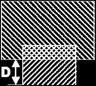
8 MUMPS Design Rules Enclosure Boundary Cut Inside Spacing Cut Outside EE C245: Introduction to MEMS Design Lecture 10 C. Nguyen 9/27/07 15 MUMPS Design Rules (cont.) Cross Sections Oxide1 Poly0 POLY0 Mask Levels ANCHOR1 EE C245: Introduction to MEMS Design Lecture 10 C. Nguyen 9/27/


 18 9")
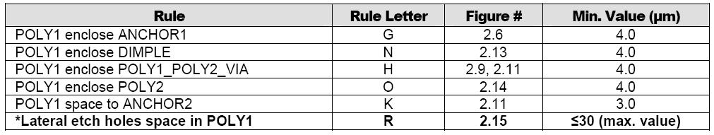
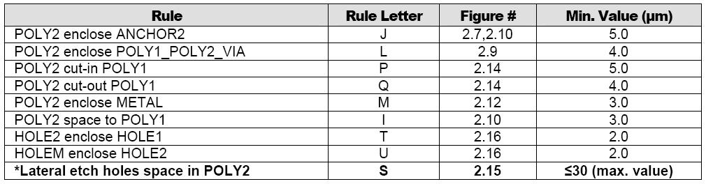
9 MUMPS Design Rules (cont.) Oxide1 Poly1 Poly0 G N H O K R Cross Sections POLY0 POLY1 Mask Levels ANCHOR1 EE C245: Introduction to MEMS Design Lecture 10 C. Nguyen 9/27/07 17 MUMPS Design Rules (cont.) EE C245: Introduction to MEMS Design Lecture 10 C. Nguyen 9/27/

10 MUMPS Design Rules (cont.) EE C245: Introduction to MEMS Design Lecture 10 C. Nguyen 9/27/07 19 The Sandia SUMMIT Process EE C245: Introduction to MEMS Design Lecture 10 C. Nguyen 9/27/

 to maintain planarity as")

 to maintain planarity as more structural layers are")
11 Sandia s SUMMiT V SUMMiT V: Sandia Ultra-planar Multi-level MEMS Technology 5 fabrication process Five-layer polysilicon surface micromachining process One electrical interconnect layer & 4 mechanical layers Uses chemical mechanical polishing (CMP) to maintain planarity as more structural layers are realized 14 masks EE C245: Introduction to MEMS Design Lecture 10 C. Nguyen 9/27/07 21 SUMMiT V Layer Stack Uses chemical mechanical polishing (CMP) to maintain planarity as more structural layers are realized EE C245: Introduction to MEMS Design Lecture 10 C. Nguyen 9/27/

 in conjunction with a polishing pad Wafer and pad are pressed together Polishing head is")


12 Chemical Mechanical Polishing (CMP) Used to planarize the top surface of a semiconductor wafer or other substrate Uses an abrasive and corrosive chemical slurry (i.e., a colloid) in conjunction with a polishing pad Wafer and pad are pressed together Polishing head is rotated with different axes of rotation (i.e., non-concentric) to randomize the polishing Top View Carrier/Chuck DI Water Side View Slurry Pad Conditioner Slurry Platen Carrier Chuck Pad Pad Conditioner Wafer Backing-Film Pad EE C245: Introduction to MEMS Design Lecture 10 C. Nguyen 9/27/07 2 CMP: Not the Same as Lapping Lapping Lapping is merely the removal of material to flatten a surface without selectivity Everything is removed at approximately the same rate Chemical Mechanical Polishing CMP is selective to certain films, and not selective to others Lapping Removes diff. materials at at same rate rate CMP Stops at at nonselective layer EE C245: Introduction to MEMS Design Lecture 10 C. Nguyen 9/27/
13 Actual SUMMiT Cross-Section No CMP until after the first three polysi layers 1 μm mmpoly1 and 1.5 μm mmpoly2 can be combined to form a 2.5 μm polysilicon film Refer to the SUMMiT V manual (one of your handouts) for more detailed information on masks and layout instructions EE C245: Introduction to MEMS Design Lecture 10 C. Nguyen 9/27/07 25 Bulk Micromachining EE C245: Introduction to MEMS Design Lecture 10 C. Nguyen 9/27/


 Process compatiblity (w/ existing layers) Safety, cost, availability, environmental impact EE C245: Introduction to MEMS Design Lecture 10 C.")
14 Bulk Micromachining Basically, etching the substrate (usually silicon) to achieve microstructures Etching modes: Isotropic vs. anisotropic Reaction-limited Etch rate dep. on temp. Diffusion-limited Etch rate dep. on mixing Also dependent on layout & geometry, i.e., on loading Choose etch mode based on Desired shape Etch depth and uniformity Surface roughness (e.g., sidewall roughness after etching) Process compatiblity (w/ existing layers) Safety, cost, availability, environmental impact EE C245: Introduction to MEMS Design Lecture 10 C. Nguyen 9/27/07 27 Mechanical Properties of Silicon Crystalline silicon is a hard and brittle material that deforms elastically until it reaches its yield strength,at which point it breaks. Tensile yield strength = 7 GPa (~1500 lb suspended from 1 mm²) Young s Modulus near that of stainless steel {100} = 10 GPa; {110} = 169 GPa; {111} = 188 GPa Mechanical properties uniform, no intrinsic stress Mechanical integrity up to 500 C Good thermal conductor Low thermal expansion coefficient High piezoresistivity EE C245: Introduction to MEMS Design Lecture 10 C. Nguyen 9/27/

 Self-limiting etches Front side mask Membrane Back side mask")
 54.")

15 Anisotropic Etching of Silicon Etching of Si w/ KOH Si + 2OH - Si(OH) e - 4H 2 O + 4e - 4(OH) - + 2H 2 Crystal orientation dependent etch rates {110}:{100}:{111}=600:400:1 {100} and {110} have 2 bonds below the surface & 2 dangling bonds that can react {111} plane has three of its bonds below the surface & only one dangling bond to react much slower E.R. {111} forms protective oxide {111} smoother than other crystal planes good for optical MEMS (mirrors) Self-limiting etches Front side mask Membrane Back side mask EE C245: Introduction to MEMS Design Lecture 10 C. Nguyen 9/27/07 29 Anisotropic Etching of Silicon Photoresist Nitride Mask Silicon Substrate Opening to Silicon Silicon Substrate <111> (100) o Silicon Substrate Deposit nitride: Target = 100nm 22 min. o C Lithography to define areas of silicon to be etched Etch/pattern nitride mask RIE using SF 6 Remove PR in PRS2000 Etch the silicon Use 1:2 KOH:H 2 O (wt.), stirred 80 C Etch Rates: (100) Si 1.4 μm/min Si N 4 ~ 0 nm/min SiO nm/min Photoresist, Al fast Micromasking by H 2 bubbles leads to roughness Stir well to displace bubbles Can also use oxidizer for (111) surfaces Or surfactant additives to suppress bubble formation EE C245: Introduction to MEMS Design Lecture 10 C. Nguyen 9/27/
![Silicon Wafers [Maluf] EE C245:](/docs-images/81/82790602/images/16-0.jpg "Introduction to MEMS Design")

: Planes Reciprocal of plane")
, intercepts: (x,y,z) =")
 (unique), {family}")

16 Silicon Wafers [Maluf] EE C245: Introduction to MEMS Design Lecture 10 C. Nguyen 9/27/07 1 Silicon Crystallography Miller Indices (h k l): Planes Reciprocal of plane intercepts with axes e.g., for (110), intercepts: (x,y,z) = (1,1, ); reciprocals: (1,1,0) (110) (unique), {family} Directions One endpoint of origin [unique], <family> EE C245: Introduction to MEMS Design Lecture 10 C. Nguyen 9/27/
![Determining Angles Between Planes The angle between vectors [abc] and [xyz] is](/docs-images/81/82790602/images/17-3.jpg "given by: ( a, b, c) ( x, y, ) cosθ ax + by + cz = z ax + by + cz θ a b c x y z =")


17 Determining Angles Between Planes The angle between vectors [abc] and [xyz] is given by: ( a, b, c) ( x, y, ) cosθ ax + by + cz = z ax + by + cz θ a b c x y z = cos 1,,,,, a, b, c x, y, z For {100} and {110} 45 o For {100} and {111} o For {110} and {111} 5.26 o, 90 o, and o ( )( ) ( ) ( ) EE C245: Introduction to MEMS Design Lecture 10 C. Nguyen 9/27/07 Silicon Crystal Origami Silicon fold-up cube Adapted from Profs. Kris Pister and Jack Judy Print onto transparency Assemble inside out Visualize crystal plane orientations, intersections, and directions [Judy, UCLA] EE C245: Introduction to MEMS Design Lecture 10 C. Nguyen 9/27/


18 Undercutting Via Anisotropic Si Etching Concave corners bounded by {111} are not attacked but convex corners bounded by {111} are attacked Two {111} planes intersecting now present two dangling bonds no longer have just one dangling bond etch rate fast Result: can undercut regions around convex corners Convex corner Suspended Beam Concave corner [Ristic] EE C245: Introduction to MEMS Design Lecture 10 C. Nguyen 9/27/07 5 Corner Compensation Protect corners with compensation areas in layout Below: Mesa array for selfassembly structures [Smith 1995] Mask pattern Shaded regions are the desired result Mask pattern EE C245: Introduction to MEMS Design Lecture 10 C. Nguyen 9/27/
EE C245 ME C218 Introduction to MEMS Design
 EE C245 ME C218 Introduction to MEMS Design Fall 2007 Prof. Clark T.-C. Nguyen Dept. of Electrical Engineering & Computer Sciences University of California at Berkeley Berkeley, CA 94720 Lecture 10: Surface
Regents of the University of California 1
 Electroplating: Metal MEMS Nickel Surface-Micromachining Process Flow Photoresist Wafer Release Etchant Use electroplating to obtain metal μstructures When thick: call it LIGA Pros: fast low temp deposition,
Regents of the University of California
 Topography Issues Degradation of lithographic resolution PR step coverage, streaking Thickness differences pose problems for reduction steppers Direction of Spin PR PR PR Stringers Problematic when using
CTN 10/1/09. EE 245: Introduction to MEMS Lecture 11: Bulk Micromachining. Copyright 2009 Regents of the University of California
 MUMPS: MultiUser MEMS ProcesS Foundry MEMS: The MUMPS Process Originally created by the Microelectronics Center of North Carolina (MCNC) now owned by MEMSCAP in France Three-level polysilicon surface micromachining
EE C245 ME C218 Introduction to MEMS Design Fall 2011
 Lecture Outline EE C245 ME C218 Introduction to MEMS Design Fall 2011 Prof. Clark T.-C. Nguyen Dept. of Electrical Engineering & Computer Sciences University of California at Berkeley Berkeley, CA 94720
EE C247B ME C218 Introduction to MEMS Design Spring 2015
 EE C247B ME C218 Introduction to MEMS Design Spring 2015 Prof. Clark T.-C. Nguyen Dept. of Electrical Engineering & Computer Sciences University of California at Berkeley Berkeley, CA 94720 Lecture EE
EE C245 ME C218 Introduction to MEMS Design Fall 2011
 EE C245 ME C218 Introduction to MEMS Design Fall 2011 Prof. Clark T.-C. Nguyen Dept. of Electrical Engineering & Computer Sciences University of California at Berkeley Berkeley, CA 94720 Lecture EE C245:
EE C247B ME C218 Introduction to MEMS Design Spring 2014
 EE C247B ME C218 Introduction to MEMS Design Spring 2014 Prof. Clark T.-C. Nguyen Dept. of Electrical Engineering & Computer Sciences University of California at Berkeley Berkeley, CA 94720 Lecture EE
EE C245 ME C218 Introduction to MEMS Design Fall 2010
 Lecture Outline EE C245 ME C218 Introduction to MEMS Design Fall 2010 Prof. Clark T.-C. Nguyen Dept. of Electrical Engineering & Computer Sciences University of California at Berkeley Berkeley, CA 94720
EE C245 ME C218 Introduction to MEMS Design Fall 2011
 Lecture Outline EE C245 ME C218 Introduction to MEMS Design Fall 2011 Prof. Clark T.-C. Nguyen Dept. of Electrical Engineering & Computer Sciences University of California at Berkeley Berkeley, CA 94720
EE C245 ME C218 Introduction to MEMS Design Fall 2010
 EE C245 ME C218 Introduction to MEMS Design Fall 2010 Prof. Clark T.-C. Nguyen Dept. of Electrical Engineering & Computer Sciences University of California at Berkeley Berkeley, CA 94720 Lecture EE C245:
4/10/2012. Introduction to Microfabrication. Fabrication
 Introduction to Microfabrication Fabrication 1 MEMS Fabrication Flow Basic Process Flow in Micromachining Nadim Maluf, An introduction to Microelectromechanical Systems Engineering 2 Thin Film Deposition
Lecture 10: MultiUser MEMS Process (MUMPS)
") MEMS: Fabrication Lecture 10: MultiUser MEMS Process (MUMPS) Prasanna S. Gandhi Assistant Professor, Department of Mechanical Engineering, Indian Institute of Technology, Bombay, 1 Recap Various VLSI based
MEMS: Fabrication Lecture 10: MultiUser MEMS Process (MUMPS) Prasanna S. Gandhi Assistant Professor, Department of Mechanical Engineering, Indian Institute of Technology, Bombay, 1 Recap Various VLSI based
EE C245 ME C218 Introduction to MEMS Design Fall 2007
 EE C245 ME C218 Introduction to MEMS Design Fall 2007 Prof. Clark T.-C. Nguyen Dept. of Electrical Engineering & Computer Sciences University of California at Berkeley Berkeley, CA 94720 Lecture 9: Surface
MEMS Fabrication I : Process Flows and Bulk Micromachining
 MEMS Fabrication I : Process Flows and Bulk Micromachining Dr. Thara Srinivasan Lecture 2 Picture credit: Alien Technology Lecture Outline Reading Reader is in! (at South side Copy Central) Kovacs, Bulk
Surface Micromachining II
 Surface Micromachining II Dr. Thara Srinivasan Lecture 4 Picture credit: Sandia National Lab Lecture Outline Reading From reader: Bustillo, J. et al., Surface Micromachining of Microelectromechanical Systems,
6.777J/2.732J Design and Fabrication of Microelectromechanical Devices Spring Term Solution to Problem Set 2 (16 pts)
") 6.777J/2.732J Design and Fabrication of Microelectromechanical Devices Spring Term 2007 By Brian Taff (Adapted from work by Feras Eid) Solution to Problem Set 2 (16 pts) Issued: Lecture 4 Due: Lecture
6.777J/2.732J Design and Fabrication of Microelectromechanical Devices Spring Term 2007 By Brian Taff (Adapted from work by Feras Eid) Solution to Problem Set 2 (16 pts) Issued: Lecture 4 Due: Lecture
Surface micromachining and Process flow part 1
 Surface micromachining and Process flow part 1 Identify the basic steps of a generic surface micromachining process Identify the critical requirements needed to create a MEMS using surface micromachining
MEMS II: January 23. Lab 1: Pop-up mirror - PolyMUMPS - Thermal actuators - Mirror CoventorWare
 MEMS II: January 23 Lab 1: Pop-up mirror - PolyMUMPS - Thermal actuators - Mirror CoventorWare Microelectromechanical Systems (MEMS) Multi-User MEMS Processes (MUMPS) Example Design Anchor hole 2.0 0.5
Welcome MNT Conference 1 Albuquerque, NM - May 2010
 Welcome MNT Conference 1 Albuquerque, NM - May 2010 Introduction to Design Outline What is MEMs Design General Considerations Application Packaging Process Flow What s available Sandia SUMMiT Overview
Lecture 5: Micromachining
 MEMS: Fabrication Lecture 5: Micromachining Prasanna S. Gandhi Assistant Professor, Department of Mechanical Engineering, Indian Institute of Technology, Bombay, Recap: Last Class E-beam lithography X-ray
Regents of the University of California
 Surface-Micromachining Process Flow Photoresist Sacrificial Oxide Structural Polysilcon Deposit sacrificial PSG: Target = 2 m 1 hr. 40 min. LPCVD @450 o C Densify the PSG Anneal @950 o C for 30 min. Lithography
Lecture 5. SOI Micromachining. SOI MUMPs. SOI Micromachining. Silicon-on-Insulator Microstructures. Agenda:
 EEL6935 Advanced MEMS (Spring 2005) Instructor: Dr. Huikai Xie SOI Micromachining Agenda: SOI Micromachining SOI MUMPs Multi-level structures Lecture 5 Silicon-on-Insulator Microstructures Single-crystal
MEMS Fabrication. Beyond Integrated Circuits. MEMS Basic Concepts
 MEMS Fabrication Beyond Integrated Circuits MEMS Basic Concepts Uses integrated circuit fabrication techniques to make mechanical as well as electrical components on a single chip. Small size 1µm 1mm Typically
Today s Class. Materials for MEMS
 Lecture 2: VLSI-based Fabrication for MEMS: Fundamentals Prasanna S. Gandhi Assistant Professor, Department of Mechanical Engineering, Indian Institute of Technology, Bombay, Recap: Last Class What is
Fabrication Technology, Part II
 EEL5225: Principles of MEMS Transducers (Fall 2003) Fabrication Technology, Part II Agenda: Process Examples TI Micromirror fabrication process SCREAM CMOS-MEMS processes Wafer Bonding LIGA Reading: Senturia,
PHYS 534 (Fall 2008) Process Integration OUTLINE. Examples of PROCESS FLOW SEQUENCES. >Surface-Micromachined Beam
 Process Integration OUTLINE. Examples of PROCESS FLOW SEQUENCES. >Surface-Micromachined Beam") PHYS 534 (Fall 2008) Process Integration Srikar Vengallatore, McGill University 1 OUTLINE Examples of PROCESS FLOW SEQUENCES >Semiconductor diode >Surface-Micromachined Beam Critical Issues in Process
PHYS 534 (Fall 2008) Process Integration Srikar Vengallatore, McGill University 1 OUTLINE Examples of PROCESS FLOW SEQUENCES >Semiconductor diode >Surface-Micromachined Beam Critical Issues in Process
EE 245: Introduction to MEMS Lecture 7m1: Lithography, Etching, & Doping CTN 9/18/ Regents of the University of California
 EE 45 Introduction to MEMS Lecture 7m1 Lithography, Etching, & Doping Anisotropic Wet Etching Anisotropic Wet Etching (cont.) Anisotropic etches also available for single crystal Can get the following
Micro-Electro-Mechanical Systems (MEMS) Fabrication. Special Process Modules for MEMS. Principle of Sensing and Actuation
 Fabrication. Special Process Modules for MEMS. Principle of Sensing and Actuation") Micro-Electro-Mechanical Systems (MEMS) Fabrication Fabrication Considerations Stress-Strain, Thin-film Stress, Stiction Special Process Modules for MEMS Bonding, Cavity Sealing, Deep RIE, Spatial forming
Micro-Electro-Mechanical Systems (MEMS) Fabrication Fabrication Considerations Stress-Strain, Thin-film Stress, Stiction Special Process Modules for MEMS Bonding, Cavity Sealing, Deep RIE, Spatial forming
Cambridge University Press A Guide to Hands-on MEMS Design and Prototyping Joel A. Kubby Excerpt More information.
 1 Introduction 1.1 Overview of MEMS fabrication Microelectromechanical systems (MEMS) fabrication developed out of the thin-film processes first used for semiconductor fabrication. To understand the unique
SOIMUMPs Design Handbook
 SOIMUMPs Design Handbook a MUMPs process C. J. Han, Allen Cowen, Greg Hames and Busbee Hardy MEMScAP Revision 3.0 Copyright 2002 by MEMScAP. All rights reserved. Permission to use and copy for internal,
Lecture 3: Integrated Processes
 Lecture 3: Integrated Processes Single-Crystal Silicon Process Integration Polysilicon Micromachining Process Integrated CMOS Micromachining Process ENE 5400, Spring 2004 1 Single Crystal Silicon ENE 5400,
Surface Micromachining
 Surface Micromachining Outline Introduction Material often used in surface micromachining Material selection criteria in surface micromachining Case study: Fabrication of electrostatic motor Major issues
Micro-Electro-Mechanical Systems (MEMS) Fabrication. Special Process Modules for MEMS. Principle of Sensing and Actuation
 Fabrication. Special Process Modules for MEMS. Principle of Sensing and Actuation") Micro-Electro-Mechanical Systems (MEMS) Fabrication Fabrication Considerations Stress-Strain, Thin-film Stress, Stiction Special Process Modules for MEMS Bonding, Cavity Sealing, Deep RIE, Spatial forming
Micro-Electro-Mechanical Systems (MEMS) Fabrication Fabrication Considerations Stress-Strain, Thin-film Stress, Stiction Special Process Modules for MEMS Bonding, Cavity Sealing, Deep RIE, Spatial forming
Lecture 7 CMOS MEMS. CMOS MEMS Processes. CMOS MEMS Processes. Why CMOS-MEMS? Agenda: CMOS MEMS: Fabrication. MEMS structures can be made
 EEL6935 Advanced MEMS (Spring 2005) Instructor: Dr. Huikai Xie CMOS MEMS Agenda: Lecture 7 CMOS MEMS: Fabrication Pre-CMOS Intra-CMOS Post-CMOS Deposition Etching Why CMOS-MEMS? Smart on-chip CMOS circuitry
ME 189 Microsystems Design and Manufacture. Chapter 9. Micromanufacturing
 ME 189 Microsystems Design and Manufacture Chapter 9 Micromanufacturing This chapter will offer an overview of the application of the various fabrication techniques described in Chapter 8 in the manufacturing
EE 330 Lecture 8. IC Fabrication Technology Part II. - Oxidation - Epitaxy - Polysilicon - Interconnects
 EE 330 Lecture 8 IC Fabrication Technology Part II - Oxidation - Epitaxy - Polysilicon - Interconnects Review from Last Time MOS Transistor Bulk Source Gate Drain p-channel MOSFET Lightly-doped n-type
Introduction to Microeletromechanical Systems (MEMS) Lecture 5 Topics. JDS Uniphase MUMPs
 Lecture 5 Topics. JDS Uniphase MUMPs") Introduction to Microeletromechanical Systems (MEMS) Lecture 5 Topics JDS Uniphase MUMPS Foundry Process and Devices Foundry Process Sequence Design Rules and Process Interactions Examples CMOS for MEMS
Introduction to Microeletromechanical Systems (MEMS) Lecture 5 Topics JDS Uniphase MUMPS Foundry Process and Devices Foundry Process Sequence Design Rules and Process Interactions Examples CMOS for MEMS
Micro-Electro-Mechanical Systems (MEMS) Fabrication. Special Process Modules for MEMS. Principle of Sensing and Actuation
 Fabrication. Special Process Modules for MEMS. Principle of Sensing and Actuation") Micro-Electro-Mechanical Systems (MEMS) Fabrication Fabrication Considerations Stress-Strain, Thin-film Stress, Stiction Special Process Modules for MEMS Bonding, Cavity Sealing, Deep RIE, Spatial forming
Micro-Electro-Mechanical Systems (MEMS) Fabrication Fabrication Considerations Stress-Strain, Thin-film Stress, Stiction Special Process Modules for MEMS Bonding, Cavity Sealing, Deep RIE, Spatial forming
Czochralski Crystal Growth
 Czochralski Crystal Growth Crystal Pulling Crystal Ingots Shaping and Polishing 300 mm wafer 1 2 Advantage of larger diameter wafers Wafer area larger Chip area larger 3 4 Large-Diameter Wafer Handling
SUMMiT V Five Level Surface Micromachining Technology Design Manual
 SUMMiT V Five Level Surface Micromachining Technology Design Manual Version 1.3 09/22/2005 MEMS Devices and Reliability Physics Department Microelectronics Development Laboratory Sandia National Laboratories
EE 330 Lecture 9. IC Fabrication Technology Part II. -Oxidation -Epitaxy -Polysilicon -Planarization -Resistance and Capacitance in Interconnects
 EE 330 Lecture 9 IC Fabrication Technology Part II -Oxidation -Epitaxy -Polysilicon -Planarization -Resistance and Capacitance in Interconnects Review from Last Time Etching Dry etch (anisotropic) SiO
Micro-Scale Engineering I Microelectromechanical Systems (MEMS) Y. C. Lee
 Y. C. Lee") Micro-Scale Engineering I Microelectromechanical Systems (MEMS) Y. C. Lee Department of Mechanical Engineering University of Colorado Boulder, CO 80309-0427 leeyc@colorado.edu September 2, 2008 1 Three
Micro-Scale Engineering I Microelectromechanical Systems (MEMS) Y. C. Lee Department of Mechanical Engineering University of Colorado Boulder, CO 80309-0427 leeyc@colorado.edu September 2, 2008 1 Three
Surface Micromachining
 Surface Micromachining Micro Actuators, Sensors, Systems Group University of Illinois at Urbana-Champaign Outline Definition of surface micromachining Most common surface micromachining materials - polysilicon
Chapter 3 Silicon Device Fabrication Technology
 Chapter 3 Silicon Device Fabrication Technology Over 10 15 transistors (or 100,000 for every person in the world) are manufactured every year. VLSI (Very Large Scale Integration) ULSI (Ultra Large Scale
Dr. Lynn Fuller Webpage:
 ROCHESTER INSTITUTE OF TECHNOLOGY MICROELECTRONIC ENGINEERING Microelectromechanical Systems (MEMs) Process Integration Dr. Lynn Fuller Webpage: http://people.rit.edu/lffeee 82 Lomb Memorial Drive Rochester,
EE 330 Lecture 9. IC Fabrication Technology Part II. -Oxidation -Epitaxy -Polysilicon -Planarization -Resistance and Capacitance in Interconnects
 EE 330 Lecture 9 IC Fabrication Technology Part II -Oxidation -Epitaxy -Polysilicon -Planarization -Resistance and Capacitance in Interconnects Review from Last Time IC Fabrication Technology Crystal Preparation
INF5490 RF MEMS. LN02: MEMS Fabrication. Spring 2012, Oddvar Søråsen Department of Informatics, UoO
 INF5490 RF MEMS LN02: MEMS Fabrication Spring 2012, Oddvar Søråsen Department of Informatics, UoO 1 Micromachining Today s lecture Important process steps General Summary: MEMS-specific steps Examples
EE 330 Lecture 9. IC Fabrication Technology Part 2
 EE 330 Lecture 9 IC Fabrication Technology Part 2 Quiz 8 A 2m silicon crystal is cut into wafers using a wire saw. If the wire diameter is 220um and the wafer thickness is 350um, how many wafers will this
EE 330 Lecture 8. IC Fabrication Technology Part II. - Masking - Photolithography - Deposition - Etching - Diffusion
 EE 330 Lecture 8 IC Fabrication Technology Part II?? - Masking - Photolithography - Deposition - Etching - Diffusion Review from Last Time Technology Files Provide Information About Process Process Flow
Proceedings Post Fabrication Processing of Foundry MEMS Structures Exhibiting Large, Out-of-Plane Deflections
 Proceedings Post Fabrication Processing of Foundry MEMS Structures Exhibiting Large, Out-of-Plane Deflections LaVern Starman 1, *, John Walton 1, Harris Hall 1 and Robert Lake 2 1 Sensors Directorate,
FABRICATION PROCESSES FOR MAGNETIC MICROACTUATORS WITH POLYSILICON FLEXURES. Jack W. Judy and Richard S. Muller
 FABRICATION PROCESSES FOR MAGNETIC MICROACTUATORS WITH POLYSILICON FLEXURES Jack W. Judy and Richard S. Muller Berkeley Sensor & Actuator Center (BSAC) Department of EECS, University of California, Berkeley,
Microfabrication of Heterogeneous, Optimized Compliant Mechanisms SUNFEST 2001 Luo Chen Advisor: Professor G.K. Ananthasuresh
 Microfabrication of Heterogeneous, Optimized Compliant Mechanisms SUNFEST 2001 Luo Chen Advisor: Professor G.K. Ananthasuresh Fig. 1. Single-material Heatuator with selective doping on one arm (G.K. Ananthasuresh)
Chemical Vapor Deposition
 Chemical Vapor Deposition ESS4810 Lecture Fall 2010 Introduction Chemical vapor deposition (CVD) forms thin films on the surface of a substrate by thermal decomposition and/or reaction of gas compounds
There are basically two approaches for bulk micromachining of. silicon, wet and dry. Wet bulk micromachining is usually carried out
 57 Chapter 3 Fabrication of Accelerometer 3.1 Introduction There are basically two approaches for bulk micromachining of silicon, wet and dry. Wet bulk micromachining is usually carried out using anisotropic
EE 434 Lecture 9. IC Fabrication Technology
 EE 434 Lecture 9 IC Fabrication Technology Quiz 7 The layout of a film resistor with electrodes A and B is shown. If the sheet resistance of the film is 40 /, determine the resistance between nodes A and
Mostafa Soliman, Ph.D. May 5 th 2014
 Mostafa Soliman, Ph.D. May 5 th 2014 Mostafa Soliman, Ph.D. 1 Basic MEMS Processes Front-End Processes Back-End Processes 2 Mostafa Soliman, Ph.D. Wafers Deposition Lithography Etch Chips 1- Si Substrate
EECS130 Integrated Circuit Devices
 EECS130 Integrated Circuit Devices Professor Ali Javey 9/13/2007 Fabrication Technology Lecture 1 Silicon Device Fabrication Technology Over 10 15 transistors (or 100,000 for every person in the world)
IC/MEMS Fabrication - Outline. Fabrication
 IC/MEMS Fabrication - Outline Fabrication overview Materials Wafer fabrication The Cycle: Deposition Lithography Etching Fabrication IC Fabrication Deposition Spin Casting PVD physical vapor deposition
CMOS Technology. Flow varies with process types & company. Start with substrate selection. N-Well CMOS Twin-Well CMOS STI
 CMOS Technology Flow varies with process types & company N-Well CMOS Twin-Well CMOS STI Start with substrate selection Type: n or p Doping level, resistivity Orientation, 100, or 101, etc Other parameters
Fabrication Technology, Part I
 EEL5225: Principles of MEMS Transducers (Fall 2003) Fabrication Technology, Part I Agenda: Oxidation, layer deposition (last lecture) Lithography Pattern Transfer (etching) Impurity Doping Reading: Senturia,
CMOS Manufacturing process. Design rule set
 CMOS Manufacturing process Circuit design Set of optical masks Fabrication process Circuit designer Design rule set Process engineer All material: Chap. 2 of J. Rabaey, A. Chandrakasan, B. Nikolic, Digital
Exam 1 Friday Sept 22
 Exam 1 Friday Sept 22 Students may bring 1 page of notes Next weeks HW assignment due on Wed Sept 20 at beginning of class No 5:00 p.m extension so solutions can be posted Those with special accommodation
Mechanical Engineering and Applied Mechanics University of Pennsylvania. A glimpse of MEMS. Presented to MEAM 550 (Fall 2001) students
 students") Mechanical Engineering and Applied Mechanics University of Pennsylvania A glimpse of MEMS Presented to MEAM 550 (Fall 2001) students G. K. Ananthasuresh September 17, 2001 What s in a name? Micro-Electro-Mechanical
Mechanical Engineering and Applied Mechanics University of Pennsylvania A glimpse of MEMS Presented to MEAM 550 (Fall 2001) students G. K. Ananthasuresh September 17, 2001 What s in a name? Micro-Electro-Mechanical
EE 143 FINAL EXAM NAME C. Nguyen May 10, Signature:
 INSTRUCTIONS Read all of the instructions and all of the questions before beginning the exam. There are 5 problems on this Final Exam, totaling 143 points. The tentative credit for each part is given to
Chapter 4 Fabrication Process of Silicon Carrier and. Gold-Gold Thermocompression Bonding
 Chapter 4 Fabrication Process of Silicon Carrier and Gold-Gold Thermocompression Bonding 4.1 Introduction As mentioned in chapter 2, the MEMs carrier is designed to integrate the micro-machined inductor
Microstructure of Electronic Materials. Amorphous materials. Single-Crystal Material. Professor N Cheung, U.C. Berkeley
 Microstructure of Electronic Materials Amorphous materials Single-Crystal Material 1 The Si Atom The Si Crystal diamond structure High-performance semiconductor devices require defect-free crystals 2 Crystallographic
Solid State Sensors. Microfabrication 8/22/08 and 8/25/08
 Solid State Sensors Microfabrication 8/22/08 and 8/25/08 Purpose of This Material To introduce the student to microfabrication techniques as used to fabricate MEMS Sensors Understand concepts not specifics
Review of CMOS Processing Technology
 - Scaling and Integration Moore s Law Unit processes Thin Film Deposition Etching Ion Implantation Photolithography Chemical Mechanical Polishing 1. Thin Film Deposition Layer of materials ranging from
5.8 Diaphragm Uniaxial Optical Accelerometer
 5.8 Diaphragm Uniaxial Optical Accelerometer Optical accelerometers are based on the BESOI (Bond and Etch back Silicon On Insulator) wafers, supplied by Shin-Etsu with (100) orientation, 4 diameter and
Mikrosensorer. Microfabrication 1
 Mikrosensorer Microfabrication 1 Literature Introductory MEMS Fabrication and Applications Thomas M. Adams and Richard A. Layton Available as ebook on http://www.lub.lu.se/en/search/lubsearch.html This
Chapter 2 OVERVIEW OF MEMS
 6 Chapter 2 OVERVIEW OF MEMS 2.1 MEMS and Microsystems The term MEMS is an abbreviation of microelectromechanical system. MEMS contains components ofsizes in 1 micrometer to 1 millimeter. The core element
INTEGRATED-CIRCUIT TECHNOLOGY
 INTEGRATED-CIRCUIT TECHNOLOGY 0. Silicon crystal growth and wafer preparation 1. Processing Steps 1.1. Photolitography 1.2. Oxidation 1.3. Layer Deposition 1.4. Etching 1.5. Diffusion 1.6 Backend: assembly,
MEMS Surface Fabrication
 ROCHESTER INSTITUTE OF TECHNOLOGY MICROELECTRONIC ENGINEERING MEMS Surface Fabrication Dr. Lynn Fuller webpage: http://people.rit.edu/lffeee Electrical and Microelectronic Engineering Rochester Institute
Process Integration. MEMS Release Techniques Sacrificial Layer Removal Substrate Undercut
 Process Integration Self-aligned Techniques LOCOS- self-aligned channel stop Self-aligned Source/Drain Lightly Doped Drain (LDD) Self-aligned silicide (SALICIDE) Self-aligned oxide gap MEMS Release Techniques
SURFACE MICROMACHINING
 SURFACE MICROMACHINING Features are built up, layer by layer on the surface of a substrate. Surface micromachined devices are much smaller than bulk micromachined components. Nature of deposition process
IC Fabrication Technology Part III Devices in Semiconductor Processes
 EE 330 Lecture 10 IC Fabrication Technology Part III Metalization and Interconnects Parasitic Capacitances Back-end Processes Devices in Semiconductor Processes Resistors Diodes Review from Last Lecture
Nonplanar Metallization. Planar Metallization. Professor N Cheung, U.C. Berkeley
 Nonplanar Metallization Planar Metallization Passivation Metal 5 (copper) Metal 3 (copper) Interlevel dielectric (ILD) Via (tungsten) Metal 1 (copper) Tungsten Plug to Si Silicon Caps and Plugs oxide oxide
Process Integration. NMOS Generic NMOS Process Flow. CMOS - The MOSIS Process Flow
 Process Integration Self-aligned Techniques LOCOS- self-aligned channel stop Self-aligned Source/Drain Lightly Doped Drain (LDD) Self-aligned silicide (SALICIDE) Self-aligned oxide gap MEMS Release Techniques
ELEC 3908, Physical Electronics, Lecture 4. Basic Integrated Circuit Processing
 ELEC 3908, Physical Electronics, Lecture 4 Basic Integrated Circuit Processing Lecture Outline Details of the physical structure of devices will be very important in developing models for electrical behavior
EE 527 MICROFABRICATION. Lecture 23 Tai-Chang Chen University of Washington
 EE 527 MICROFABRICATION Lecture 23 Tai-Chang Chen University of Washington SILICON CRYSTAL STRUCTURE Silicon atoms in a crystal lattice are regularly arranged in a lattice structure. Material properties,
ASIM-X MEMS-Specific Design Rules
 ASIM-X MEMS-Specific Design Rules Version 2 Revised April 5, 2006. This is a beta version, subject to change. Revised by G. K. Fedder, Carnegie Mellon University. 1 Process Overview ASIM-X, an acronym
Lect. 2: Basics of Si Technology
 Unit processes Thin Film Deposition Etching Ion Implantation Photolithography Chemical Mechanical Polishing 1. Thin Film Deposition Layer of materials ranging from fractions of nanometer to several micro-meters
PolyMUMPs FAQ, v2.0. a MUMPs process MEMSCAP. Revision 2.0
 PolyMUMPs FAQ a MUMPs process MEMSCAP Revision 2.0 1 Copyright 2004 by MEMSCAP. All rights reserved. Permission to use and copy for internal, noncommercial purposes is hereby granted. Any distribution
3.155J / 6.152J Micro/Nano Processing Technology TAKE-HOME QUIZ FALL TERM 2005
 3.155J / 6.152J Micro/Nano Processing Technology TAKE-HOME QUIZ FALL TERM 2005 1) This is an open book, take-home quiz. You are not to consult with other class members or anyone else. You may discuss the
ECE321 Electronics I
 ECE321 Electronics I Lecture 19: CMOS Fabrication Payman Zarkesh-Ha Office: ECE Bldg. 230B Office hours: Tuesday 2:00-3:00PM or by appointment E-mail: payman@ece.unm.edu Slide: 1 Miller Effect Interconnect
EE C245 / ME C Cory. symmetric in both. polysilicon.
 PROBLEM SET #6 Issued: Thursday, Nov. 4, 2010. Due (at 7 p.m.): Tuesday, Nov. 23, 2010, in the EE C2455 HW box in 240 Cory. 1. Suppose you would like to fabricate the folded-beam suspended comb-driven
Fabrication Process. Crystal Growth Doping Deposition Patterning Lithography Oxidation Ion Implementation CONCORDIA VLSI DESIGN LAB
 Fabrication Process Crystal Growth Doping Deposition Patterning Lithography Oxidation Ion Implementation 1 Fabrication- CMOS Process Starting Material Preparation 1. Produce Metallurgical Grade Silicon
The Physical Structure (NMOS)
") The Physical Structure (NMOS) Al SiO2 Field Oxide Gate oxide S n+ Polysilicon Gate Al SiO2 SiO2 D n+ L channel P Substrate Field Oxide contact Metal (S) n+ (G) L W n+ (D) Poly 1 3D Perspective 2 3 Fabrication
The Physical Structure (NMOS) Al SiO2 Field Oxide Gate oxide S n+ Polysilicon Gate Al SiO2 SiO2 D n+ L channel P Substrate Field Oxide contact Metal (S) n+ (G) L W n+ (D) Poly 1 3D Perspective 2 3 Fabrication
L5: Micromachining processes 1/7 01/22/02
 97.577 L5: Micromachining processes 1/7 01/22/02 5: Micromachining technology Top-down approaches to building large (relative to an atom or even a transistor) structures. 5.1 Bulk Micromachining A bulk
Chapter 3 CMOS processing technology
 Chapter 3 CMOS processing technology (How to make a CMOS?) Si + impurity acceptors(p-type) donors (n-type) p-type + n-type => pn junction (I-V) 3.1.1 (Wafer) Wafer = A disk of silicon (0.25 mm - 1 mm thick),
Lecture 0: Introduction
 Lecture 0: Introduction Introduction Integrated circuits: many transistors on one chip. Very Large Scale Integration (VLSI): bucketloads! Complementary Metal Oxide Semiconductor Fast, cheap, low power
PiezoMUMPs Design Handbook
 PiezoMUMPs Design Handbook a MUMPs process Allen Cowen, Greg Hames, Konstantin Glukh, and Busbee Hardy MEMSCAP Inc. Revision 1.3 Copyright 2014 by MEMSCAP Inc.,. All rights reserved. Permission to use
Chemical Mechanical Planarization
 1 Chemical Mechanical Planarization SFR Workshop & Review November 14, 2002 David Dornfeld, Fiona Doyle, Costas Spanos, Jan Talbot Berkeley, CA 2 Focus of this presentation CMP research milestones in SFR
CSCI 4974 / 6974 Hardware Reverse Engineering. Lecture 5: Fabrication processes
 CSCI 4974 / 6974 Hardware Reverse Engineering Lecture 5: Fabrication processes QUIZ 3: CMOS layout Quiz Discussion Rationale If you know how something is put together, you can figure out how to take it
EE40 Lec 22. IC Fabrication Technology. Prof. Nathan Cheung 11/19/2009
 Suggested Reading EE40 Lec 22 IC Fabrication Technology Prof. Nathan Cheung 11/19/2009 300mm Fab Tour http://www-03.ibm.com/technology/manufacturing/technology_tour_300mm_foundry.html Overview of IC Technology
Supporting Information
 Supporting Information Fast-Response, Sensitivitive and Low-Powered Chemosensors by Fusing Nanostructured Porous Thin Film and IDEs-Microheater Chip Zhengfei Dai,, Lei Xu,#,, Guotao Duan *,, Tie Li *,,
PROCESS FLOW AN INSIGHT INTO CMOS FABRICATION PROCESS
 Contents: VI Sem ECE 06EC63: Analog and Mixed Mode VLSI Design PROCESS FLOW AN INSIGHT INTO CMOS FABRICATION PROCESS 1. Introduction 2. CMOS Fabrication 3. Simplified View of Fabrication Process 3.1 Alternative
Integrated Processes. Lecture Outline
 Integrated Processes Thara Srinivasan Lecture 14 Picture credit: Lemkin et al. Lecture Outline From reader Bustillo, J. et al., Surface micromachining of MEMS, pp. 1556-9. A.E. Franke et al., Polycrystalline