Development of High Voltage Silicon Carbide MOSFET Devices in KERI
|
|
|
- Dwain Black
- 5 years ago
- Views:
Transcription


1 Development of High Voltage Silicon Carbide MOSFET Devices in KERI Kim, Sang Cheol Power Semiconductor Device Research Center Korea Electrotechnology Research Institute
2 Contents Introduction Why Silicon Carbide Semiconductors? Power Semiconductor Research Activities in KERI Power Semiconductor Key Technologies Silicon Carbide Power MOSFET Design Silicon Carbide Power MOSFET Fabrication Results Summary & Future Works
3 Introduction Global environmental and energy problem Improve the levels of efficiency of power converters The characteristics of Si power devices have almost reached their theoretical limitations, and further improvements are now becoming difficult to achieve. Performance limit of Power Devices


4 Introduction EV Power Consumer Appliance SiC Device Aero- Space -High Voltage -High Frequency -High Temperature Industial Nuclear -High Density -Radiation -Low Loss Potential Application of SiC Devices Requirements
5 Why SiC Semiconductors? SiC exhibits a power density possibly one order of magnitude or more compared to silicon. - Current density can easily reach 5 to 10A/mm 2 - Breakdown voltage(volt/um of epilayer) is typically in the 100V/um for SiC (10V/um for Silicon) A single SiC device will drive higher current and voltage in a reduced footprint. SiC is intrinsically very high thermal conductive material. Higher electron mobility of SiC also permits higher frequency operation in switching mode.


6 Power Semiconductor Research Activities in KERI SiC Epitaxy 600V SiC SBD 2000V SiC PN Diode SiC Wafer Defect Analysis Si Dynistor Si IGCT 600V SiC VDMOSFET 1200V SiC VDMOSFET 2500V SiC VDMOSFET
7 Power Semiconductor Key Tech. Process High resolution - <0.5 um process - 64M DRAM equiv. Trench process - Surface roughness - Deep & High aspect ratio - Uniformity Thin wafer technology -Thin wafer handling - Grinding/ Roughness /damaged layer removal - High energy implantation - Low temp. activation emitter gate n+ P - base n- n0 FS layer p-layer collector Design High Performance - Tighter & Optimized active cell design - Channel/trench design for the short circuit capability High voltage - Design the thickness & concentration - Reliable high BV Junction termination High efficiency - Control injection efficiency


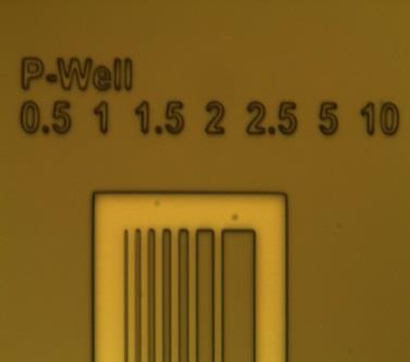
8 1.2kV SiC Power MOSFET Design BV=1200V Tepi > 15um Cepi < 2E15cm -3 Junc. Depth ~0.5um Cp-base > 4E17cm -3 Epi-layer Selection P-base Design VT < 5V Csurface < 7E16cm -3 Retrograde profile JFET : 2~4um Threshold Voltage Design On-resistance Design
 : 7E16/ cm3 P-well")

9 1.2kV SiC Power MOSFET Design N-Sub Concentration : 1E19/ cm3 N-Epi Concentration : 2E15/ cm3 N-Epi Thickness : 15um P-well Concentration(surface) : 7E16/ cm3 P-well Concentration(junction) : 4E17/ cm3 P-well Junction Depth : 0.5~0.7um N-Source Concentration : 1E19/ cm3 N-Source Junction Depth : 0.2um Channel length : 0.5~2.0um JFET Width : 2~4um # of Fleid Limiting Ring : 8
10 SiC Power MOSFET Fabrication Initial oxidation Align key PHOTO Align key ETCH Oxidation P-Well Photo P-Well ETCH P-Well IMP EPI inspection Cleaning Oxidation PR Coat Exposure Develop Etch ashing PR Romove Cleaning Oxide depo PR coat Exposure Develop Pwell Etch Ashing PR Remove P-well I/I Oxide strip Oxidation P+ photo P+ ETCH P+ IMP Oxidation N+ photo N+ ETCH N+ IMP Cleaning Oxide depo PR Coat Exposure Develop Pwell Etch Ashing PR Remove P-Well I/I Oxide strip Cleaning Oxide depo PR Coat Exposure Develop Pwell Etch Ashing PR Remove N+ I/I Cleaning Activation anneal Gate OX Poly Poly PHOTO Poly ETCH PECVD deposition CNT Photo Contact Etch POLY back etch annel 1 st Sac. Ox. Oxide strip Cleaning Gate Ox. Poly Depo 검사 PR Coat Exposure Develop Poly Etch Ashing PR Remove Cleaning PSG depo PR Coat Exposure Develop Etch Ashing PR Remove Poly Etch Silicide metal deposition Back metal depo Silicide photo Silicide etch Silicidation Front metal MET PHOTO Metal Etch Cleaning Depo Cleaning Depo PR Coat Exposure Develop wet etch PR strip RTA Cleaning Depo PR Coat Exposure Develop Etch Dust Etch Ashing
![Concentration [atomic/cm 3 ] Intensity [cps] Key Process in KERI Ion Implantation Condition 1E22 1E21 10 7 10 6 1E20 1E19 1E18 1E17 1E16 1E15 14N 27Al 12C 30Si 10 5 10 4 10 3 10 2 10 1](/docs-images/81/83648925/images/11-0.jpg "1E14 10 0 0 500 1000 1500 2000 Depth Profile [nm] P-Well Ion implantation : Junction depth = 0.6~0.8um Retrograde profile N-Source Ion implantation : Junction depth = 0.2~0.")
11 Concentration [atomic/cm 3 ] Intensity [cps] Key Process in KERI Ion Implantation Condition 1E22 1E E20 1E19 1E18 1E17 1E16 1E15 14N 27Al 12C 30Si E Depth Profile [nm] P-Well Ion implantation : Junction depth = 0.6~0.8um Retrograde profile N-Source Ion implantation : Junction depth = 0.2~0.25um Box profile


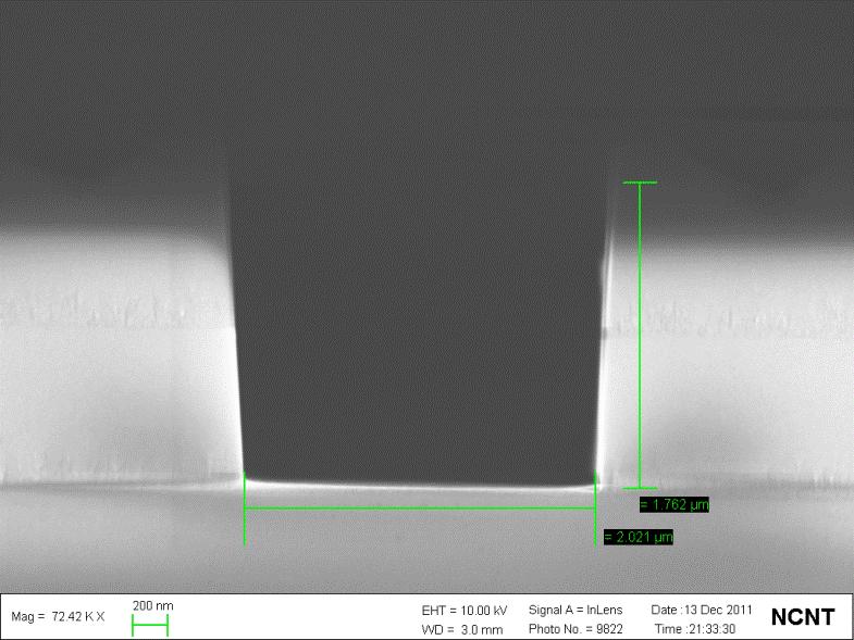
12 Key Process in KERI Hard Mask for Ion Implantation PR SiO 2 Precision < 0.5um Etching angle > 83
13 Key Process in KERI Gate Oxidation & Post Oxide Annealing Gate Oxide Condition : 1150 /5hr/Dry O 2 : 55nm Post Oxide Annealing Condition : 1175 /0~3hr/NO Concentration Interface Trap Density : POA Conduction Band Edge) CN & SiN Intensity : 100% NO POA TOF-SIMS analysis)
 0hr NO Annealing 1hr NO Annealing 2hr NO Annealing 3hr NO")


14 Key Process in KERI Gate Oxidation & Post Oxide Annealing (Time Zero Dielectric Breakdown Characteristics) 0hr NO Annealing 1hr NO Annealing 2hr NO Annealing 3hr NO Annealing Dielectric breakdown and leakage current characteristics were improved at 3hr NO annealing condition. 3hr NO post annealing was shown excellent result in Gate oxide reliability characteristics by constant voltage stress test From those results, 1175 /3hr NO annealing is best condition for Carbon restriction at SiO 2 -SiC interface.

15 Contact Silicide Key Process in KERI N-type Ohmic Contact P-type Ohmic Contact Target of this contact process Simultaneous N- & P-Ohmic Contact condition Conventional Simple Process condition Ti/Ni is good candidate metal for low contact resistance.


16 Results 4inch SiC Wafer & MOSFET Devices SiC MOSFET Package
17 Results Forward Characteristics Forward I-V Characteristics ( VG=5V) Threshold Voltage(VTH) Characteristic

 ~")
18 Results Gate Oxide Quality GOX Quality Interface Trap Density (Dit) < 1E11cm -2 ev -1 Maximum Breakdown Field of Oxide (E C ) ~ 7MV/cm
19 Results Reverse Characteristics Strong dependence on Field Limiting Ring(FLR) space Several na s leakage characteristics Superior reverse characteristics on FLR + FP structure 6 FLR is enough to 1200V breakdown voltage

20 Switching Characteristics Results Test circuit & waveform Test board T R : 874ns T D : 210ns E on : 286uJ T F : 64ns T D : 21ns E off : 21.1uJ Turn-on waveform Turn-off waveform
21 Results Fabrication Yield 1 st stage yield < 30% Device (2 nd stage) Total Operate device Yield rate 2 nd stage yield > 60% #910_10A % 312 #920_10A % Device (3 rd stage) Total 3 rd stage yield > 70% Operate device Yield rate #10_2_10A %
22 Summary & Future Plan We developed successfully 1200V/40A high voltage SiC MOSFET devices. Design & Fabrication processes are carried out Maximum breakdown voltage is exceeded 1700V. On-state resistance characteristics are less than 55mΩ cm 2. Current density is 187A/ cm 2. Design & fabrication technology were transferred to semiconductor company. Our future plan is develop 15kV high voltage SiC MOSFET devices next 5 years for HVDC system.
23 Thank you very much for your attention
SiC high voltage device development
 SiC high voltage device development 2006. 11. 30 KERI Power Semiconductor Group outline 1. Device design & simulation for power devices 2. SiC power diode process development Ion implantation & activation
Isolation Technology. Dr. Lynn Fuller
 ROCHESTER INSTITUTE OF TECHNOLOGY MICROELECTRONIC ENGINEERING Isolation Technology Dr. Lynn Fuller Motorola Professor 82 Lomb Memorial Drive Rochester, NY 14623-5604 Tel (585) 475-2035 Fax (585) 475-5041
EE 330 Lecture 9. IC Fabrication Technology Part 2
 EE 330 Lecture 9 IC Fabrication Technology Part 2 Quiz 8 A 2m silicon crystal is cut into wafers using a wire saw. If the wire diameter is 220um and the wafer thickness is 350um, how many wafers will this
Development of Silicon Pad and Strip Detector in High Energy Physics
 XXI DAE-BRNS High Energy Physics Symposium 2014, IIT Guwahati Development of Silicon Pad and Strip Detector in High Energy Physics Manoj Jadhav Department of Physics I.I.T. Bombay 2 Manoj Jadhav, IIT Bombay.
Chapter 3 CMOS processing technology
 Chapter 3 CMOS processing technology (How to make a CMOS?) Si + impurity acceptors(p-type) donors (n-type) p-type + n-type => pn junction (I-V) 3.1.1 (Wafer) Wafer = A disk of silicon (0.25 mm - 1 mm thick),
EE 330 Lecture 9. IC Fabrication Technology Part II. -Oxidation -Epitaxy -Polysilicon -Planarization -Resistance and Capacitance in Interconnects
 EE 330 Lecture 9 IC Fabrication Technology Part II -Oxidation -Epitaxy -Polysilicon -Planarization -Resistance and Capacitance in Interconnects Review from Last Time IC Fabrication Technology Crystal Preparation
Lecture 22: Integrated circuit fabrication
 Lecture 22: Integrated circuit fabrication Contents 1 Introduction 1 2 Layering 4 3 Patterning 7 4 Doping 8 4.1 Thermal diffusion......................... 10 4.2 Ion implantation.........................
Fairchild Semiconductor Application Note June 1983 Revised March 2003
 Fairchild Semiconductor Application Note June 1983 Revised March 2003 High-Speed CMOS (MM74HC) Processing The MM74HC logic family achieves its high speed by utilizing microcmos Technology. This is a 3.5
Czochralski Crystal Growth
 Czochralski Crystal Growth Crystal Pulling Crystal Ingots Shaping and Polishing 300 mm wafer 1 2 Advantage of larger diameter wafers Wafer area larger Chip area larger 3 4 Large-Diameter Wafer Handling
EE 434 Lecture 9. IC Fabrication Technology
 EE 434 Lecture 9 IC Fabrication Technology Quiz 7 The layout of a film resistor with electrodes A and B is shown. If the sheet resistance of the film is 40 /, determine the resistance between nodes A and
EE 330 Lecture 8. IC Fabrication Technology Part II. - Oxidation - Epitaxy - Polysilicon - Interconnects
 EE 330 Lecture 8 IC Fabrication Technology Part II - Oxidation - Epitaxy - Polysilicon - Interconnects Review from Last Time MOS Transistor Bulk Source Gate Drain p-channel MOSFET Lightly-doped n-type
CMOS Technology. Flow varies with process types & company. Start with substrate selection. N-Well CMOS Twin-Well CMOS STI
 CMOS Technology Flow varies with process types & company N-Well CMOS Twin-Well CMOS STI Start with substrate selection Type: n or p Doping level, resistivity Orientation, 100, or 101, etc Other parameters
EE 143 FINAL EXAM NAME C. Nguyen May 10, Signature:
 INSTRUCTIONS Read all of the instructions and all of the questions before beginning the exam. There are 5 problems on this Final Exam, totaling 143 points. The tentative credit for each part is given to
EE 330 Lecture 9. IC Fabrication Technology Part II. -Oxidation -Epitaxy -Polysilicon -Planarization -Resistance and Capacitance in Interconnects
 EE 330 Lecture 9 IC Fabrication Technology Part II -Oxidation -Epitaxy -Polysilicon -Planarization -Resistance and Capacitance in Interconnects Review from Last Time Etching Dry etch (anisotropic) SiO
Amorphous and Polycrystalline Thin-Film Transistors
 Part I Amorphous and Polycrystalline Thin-Film Transistors HYBRID AMORPHOUS AND POLYCRYSTALLINE SILICON DEVICES FOR LARGE-AREA ELECTRONICS P. Mei, J. B. Boyce, D. K. Fork, G. Anderson, J. Ho, J. Lu, Xerox
Lecture 030 Integrated Circuit Technology - I (5/8/03) Page 030-1
 Page 030-1") Lecture 030 Integrated Circuit Technology - I (5/8/03) Page 030-1 LECTURE 030 INTEGRATED CIRCUIT TECHNOLOGY - I (References [7,8]) Objective The objective of this presentation is: 1.) Illustrate integrated
Lecture 030 Integrated Circuit Technology - I (5/8/03) Page 030-1 LECTURE 030 INTEGRATED CIRCUIT TECHNOLOGY - I (References [7,8]) Objective The objective of this presentation is: 1.) Illustrate integrated
Andrei P. MIHAILA Suhail R. JEREMY Florin UDREA Gehan A. J. AMARATUNGA
 Rajesh Kumar MALHAN Yuuichi TAKEUCHI Mitsuhiro KATAOKA Andrei P. MIHAILA Suhail R. JEREMY Florin UDREA Gehan A. J. AMARATUNGA A double gate normally-off silicon carbide (SiC) trench junction field effect
MOS Front-End. Field effect transistor
 MOS Front-End Back-end Transistor Contact Front-end p-well STI n-well Front-end-of-line includes substrate, isolation, wells, transistor, silicide Field effect transistor MOSFET: Metal-Oxide-Semiconductor
Characteristics of HfO 2 pmosfet with Ultrashallow Junction Prepared by Plasma Doping and Laser Annealing
 Characteristics of HfO 2 pmosfet with Ultrashallow Junction Prepared by Plasma Doping and Laser Annealing Sungkweon Baek, Sungho Heo, and Hyunsang Hwang Dept. of Materials Science and Engineering Kwangju
Synchrotron X-Ray Topography Measurements on 4H-SiC Epitaxial Layer
 Synchrotron X-Ray Topography Measurements on 4H-SiC Epitaxial Layer Isaho KAMATA, Central Research Institute of Electric Power Industry (CRIEPI) Kamata@criepi.denken.or.jp Silicon carbide has excellent
Chapter 3 Silicon Device Fabrication Technology
 Chapter 3 Silicon Device Fabrication Technology Over 10 15 transistors (or 100,000 for every person in the world) are manufactured every year. VLSI (Very Large Scale Integration) ULSI (Ultra Large Scale
Microstructure of Electronic Materials. Amorphous materials. Single-Crystal Material. Professor N Cheung, U.C. Berkeley
 Microstructure of Electronic Materials Amorphous materials Single-Crystal Material 1 The Si Atom The Si Crystal diamond structure High-performance semiconductor devices require defect-free crystals 2 Crystallographic
Resistive switching of CeO x /SiO 2 stacked film based on anodic oxidation and breakdown
 Feb. 19 th, 2015 WIMNACT-45 Resistive switching of /SiO 2 stacked film based on anodic oxidation and breakdown K. Kakushima Tokyo Institute of Technology 1 Introduction to resistive RAM (RRAM) Reset OFF
VLSI Technology Dr. Nandita Dasgupta Department of Electrical Engineering Indian Institute of Technology, Madras
 VLSI Technology Dr. Nandita Dasgupta Department of Electrical Engineering Indian Institute of Technology, Madras Lecture - 33 Problems in LOCOS + Trench Isolation and Selective Epitaxy So, we are discussing
Process Integration. MEMS Release Techniques Sacrificial Layer Removal Substrate Undercut
 Process Integration Self-aligned Techniques LOCOS- self-aligned channel stop Self-aligned Source/Drain Lightly Doped Drain (LDD) Self-aligned silicide (SALICIDE) Self-aligned oxide gap MEMS Release Techniques
Quarterly Report EPRI Agreement W
 Quarterly Report EPRI Agreement W08069-07 PI: S.J. Pearton, University of Florida (Co-investigators F. Ren, C.R. Abernathy, R.K. Singh, P.H. Holloway, T.J. Anderson, M. Berding, A. Sher, S. Krishnimurthy,
Doping and Oxidation
 Technische Universität Graz Institute of Solid State Physics Doping and Oxidation Franssila: Chapters 13,14, 15 Peter Hadley Technische Universität Graz Institute of Solid State Physics Doping Add donors
Annual Meeting. North Carolina State University Dr. Veena Misra. January 17 19, 2017 December
 Annual Meeting North Carolina State University Dr. Veena Misra January 17 19, 2017 December 8 2015 1 Misra Group at NCSU Over 9 years experience in wide band gap research on SiC, GaN and Ga2O3. World leaders
Make sure the exam paper has 9 pages total (including cover page)
") UNIVERSITY OF CALIFORNIA College of Engineering Department of Electrical Engineering and Computer Sciences Fall 2010 EE143 Midterm Exam #2 Family Name First name SID Signature Solution Make sure the exam
UNIVERSITY OF CALIFORNIA College of Engineering Department of Electrical Engineering and Computer Sciences Fall 2010 EE143 Midterm Exam #2 Family Name First name SID Signature Solution Make sure the exam
Review of CMOS Processing Technology
 - Scaling and Integration Moore s Law Unit processes Thin Film Deposition Etching Ion Implantation Photolithography Chemical Mechanical Polishing 1. Thin Film Deposition Layer of materials ranging from
HOMEWORK 4 and 5. March 15, Homework is due on Monday March 30, 2009 in Class. Answer the following questions from the Course Textbook:
 HOMEWORK 4 and 5 March 15, 2009 Homework is due on Monday March 30, 2009 in Class. Chapter 7 Answer the following questions from the Course Textbook: 7.2, 7.3, 7.4, 7.5, 7.6*, 7.7, 7.9*, 7.10*, 7.16, 7.17*,
Fabrication and Layout
 Fabrication and Layout Kenneth Yun UC San Diego Adapted from EE271 notes, Stanford University Overview Semiconductor properties How chips are made Design rules for layout Reading Fabrication: W&E 3.1,
Fabrication of high power GaN transistors F. Medjdoub CNRS - IEMN
 Fabrication of high power GaN transistors F. Medjdoub CNRS - IEMN E. Dogmus, A. Linge, T. Defais, R. Kabouche, R. Pecheux, M. Zegaoui Lille city centre Where are we? National Network of Large Technological
A Proposal of Schottky Barrier Height Tuning Method with Interface controlled Ni/Si stacked Silicidation Process
 222 nd ECS Meeting A Proposal of Schottky arrier Height Tuning Method with Interface controlled Ni/Si stacked Silicidation Process Y. Tamura 1, R. Yoshihara 1, K. Kakushima 2, P. Ahmet 1, Y. Kataoka 2,
Microelettronica. Planar Technology for Silicon Integrated Circuits Fabrication. 26/02/2017 A. Neviani - Microelettronica
 Microelettronica Planar Technology for Silicon Integrated Circuits Fabrication 26/02/2017 A. Neviani - Microelettronica Introduction Simplified crosssection of an nmosfet and a pmosfet Simplified crosssection
Chapter 2 Problems. The CMOS technology we need to realize is shown below, from Figure 1-34 in the text. S P + N P + N WELL P +
 Chapter 2 roblems 2.1 Sketch a process flow that would result in the structure shown in Figure 1-34 by drawing a series of drawings similar to those in this chapter. You only need to describe the flow
EE 143 MICROFABRICATION TECHNOLOGY FALL 2014 C. Nguyen PROBLEM SET #9
 Issued: Tuesday, Nov. 11, 2014 PROBLEM SET #9 Due: Wednesday, Nov. 19, 2010, 8:00 a.m. in the EE 143 homework box near 140 Cory 1. The following pages comprise an actual pwell CMOS process flow with poly-to-poly
Department of Electrical Engineering. Jungli, Taiwan
 Chapter 3 Fabrication of CMOS Integrated Circuits Jin-Fu Li Department of Electrical Engineering National Central University Jungli, Taiwan Background Outline The CMOS Process Flow Design Rules Latchup
MOS interface processing and properties utilizing Ba-interface layers
 MOS interface processing and properties utilizing Ba-interface layers Daniel J. Lichtenwalner, Vipindas Pala, Brett Hull, Scott Allen, & John W. Palmour Power R&D, Cree, Inc. Durham, NC 27703 Partial funding
3.155J / 6.152J Micro/Nano Processing Technology TAKE-HOME QUIZ FALL TERM 2005
 3.155J / 6.152J Micro/Nano Processing Technology TAKE-HOME QUIZ FALL TERM 2005 1) This is an open book, take-home quiz. You are not to consult with other class members or anyone else. You may discuss the
Microelectronic Device Instructional Laboratory. Table of Contents
 Introduction Process Overview Microelectronic Device Instructional Laboratory Introduction Description Flowchart MOSFET Development Process Description Process Steps Cleaning Solvent Cleaning Photo Lithography
VLSI INTRODUCTION P.VIDYA SAGAR ( ASSOCIATE PROFESSOR) Department of Electronics and Communication Engineering, VBIT
 Department of Electronics and Communication Engineering, VBIT") VLSI INTRODUCTION P.VIDYA SAGAR ( ASSOCIATE PROFESSOR) contents UNIT I INTRODUCTION: Introduction to IC Technology MOS, PMOS, NMOS, CMOS & BiCMOS technologies. BASIC ELECTRICAL PROPERTIES : Basic Electrical
VLSI INTRODUCTION P.VIDYA SAGAR ( ASSOCIATE PROFESSOR) contents UNIT I INTRODUCTION: Introduction to IC Technology MOS, PMOS, NMOS, CMOS & BiCMOS technologies. BASIC ELECTRICAL PROPERTIES : Basic Electrical
EE 330 Lecture 12. Devices in Semiconductor Processes
 EE 330 Lecture 12 Devices in Semiconductor Processes Review from Lecture 9 Copper Interconnects Limitations of Aluminum Interconnects Electromigration Conductivity not real high Relevant Key Properties
AIST, 2 CREST/AIST, 3 Univ. Of Tsukuba
 A. Traoré 1, A. Nakajima 1, T. Makino 1,2, D. Kuwabara 1,2,3, H. Kato 1,2, M. Ogura 1,2, D. Takeuchi 1,2, and S. Yamasaki 1,2,3 1 AIST, 2 CREST/AIST, 3 Univ. Of Tsukuba aboulaye.traore@aist.go.jp Diamond
MOLYBDENUM AS A GATE ELECTRODE FOR DEEP SUB-MICRON CMOS TECHNOLOGY
 Mat. Res. Soc. Symp. Vol. 611 2000 Materials Research Society MOLYBDENUM AS A GATE ELECTRODE FOR DEEP SUB-MICRON CMOS TECHNOLOGY Pushkar Ranade, Yee-Chia Yeo, Qiang Lu, Hideki Takeuchi, Tsu-Jae King, Chenming
Isolation of elements
 1 In an IC, devices on the same substrate must be isolated from one another so that there is no current conduction between them. Isolation uses either the junction or dielectric technique or a combination
Semiconductor Devices
 Semiconductor Devices - 2014 Lecture Course Part of SS Module PY4P03 Dr. P. Stamenov School of Physics and CRANN, Trinity College, Dublin 2, Ireland Hilary Term, TCD 20 th of Jan 14 M-S and p-n Junctions
FABRICATION of MOSFETs
 FABRICATION of MOSFETs CMOS fabrication sequence -p-type silicon substrate wafer -creation of n-well regions for pmos transistors, -impurity implantation into the substrate. -thick oxide is grown in the
Design Consideration and Effect of Parameter Variation on sub-40nm Bulk MOSFET using TCAD Tool
 International Journal of Electronics and Communication Engineering. ISSN 0974-2166 Volume 4, Number 3 (2011), pp. 267-274 International Research Publication House http://www.irphouse.com Design Consideration
Simple Cubic Crystal
 Starting Material Simple Cubic Crystal Crystal Planes offset by d/4 Diamond lattice cell (C, Si, Ge, etc.) face atom in FCC corner atom in FCC (100) plane (110) plane (111) plane Crystal Planes/Direction
Chapter 4 : ULSI Process Integration (0.18 m CMOS Process)
") Chapter : ULSI Process Integration (0.8 m CMOS Process) Reference. Semiconductor Manufacturing Technology : Michael Quirk and Julian Serda (00). - (00). Semiconductor Physics and Devices- Basic Principles(/e)
Chapter : ULSI Process Integration (0.8 m CMOS Process) Reference. Semiconductor Manufacturing Technology : Michael Quirk and Julian Serda (00). - (00). Semiconductor Physics and Devices- Basic Principles(/e)
A discussion of crystal growth, lithography, etching, doping, and device structures is presented in
 Chapter 5 PROCESSING OF DEVICES A discussion of crystal growth, lithography, etching, doping, and device structures is presented in the following overview gures. SEMICONDUCTOR DEVICE PROCESSING: AN OVERVIEW
Complementary Metal Oxide Semiconductor (CMOS)
") Technische Universität Graz Institute of Solid State Physics Complementary Metal Oxide Semiconductor (CMOS) Franssila: Chapters 26,28 Technische Universität Graz Institute of Solid State Physics Complementary
Technische Universität Graz Institute of Solid State Physics Complementary Metal Oxide Semiconductor (CMOS) Franssila: Chapters 26,28 Technische Universität Graz Institute of Solid State Physics Complementary
Lect. 2: Basics of Si Technology
 Unit processes Thin Film Deposition Etching Ion Implantation Photolithography Chemical Mechanical Polishing 1. Thin Film Deposition Layer of materials ranging from fractions of nanometer to several micro-meters
IC Fabrication Technology Part III Devices in Semiconductor Processes
 EE 330 Lecture 10 IC Fabrication Technology Part III Metalization and Interconnects Parasitic Capacitances Back-end Processes Devices in Semiconductor Processes Resistors Diodes Review from Last Lecture
Process Integration. NMOS Generic NMOS Process Flow. CMOS - The MOSIS Process Flow
 Process Integration Self-aligned Techniques LOCOS- self-aligned channel stop Self-aligned Source/Drain Lightly Doped Drain (LDD) Self-aligned silicide (SALICIDE) Self-aligned oxide gap MEMS Release Techniques
Amorphous silicon / crystalline silicon heterojunction solar cell
 Workshop on "Physics for Renewable Energy" October 17-29, 2005 301/1679-9 "Amorphous Silicon / Cyrstalline Silicon Heterojunction Solar Cell" E. Centurioni CNR/IMM AREA Science Park - Bologna Italy Amorphous
CMOS FABRICATION. n WELL PROCESS
 CMOS FABRICATION n WELL PROCESS Step 1: Si Substrate Start with p- type substrate p substrate Step 2: Oxidation Exposing to high-purity oxygen and hydrogen at approx. 1000 o C in oxidation furnace SiO
Mark T. Bohr Intel Senior Fellow, Technology and Manufacturing Group Director, Process Architecture and Integration INTEL CORPORATION
 Mark T. Bohr Intel Senior Fellow, Technology and Manufacturing Group Director, Process Architecture and Integration INTEL CORPORATION Patents» 6762464, N-P butting connections on SOI substrates, 7/13/2004.»
Silicon Epitaxial CVD Want to create very sharp PN boundary grow one type layer on other in single crystal form High dopant layers on low dopant
 Silicon Epitaxial CVD Want to create very sharp PN boundary grow one type layer on other in single crystal form High dopant layers on low dopant substrate Creates latch up protection for CMOS Buried Epi
EE 330 Lecture 8. IC Fabrication Technology Part II. - Masking - Photolithography - Deposition - Etching - Diffusion
 EE 330 Lecture 8 IC Fabrication Technology Part II?? - Masking - Photolithography - Deposition - Etching - Diffusion Review from Last Time Technology Files Provide Information About Process Process Flow
Is Now Part of To learn more about ON Semiconductor, please visit our website at
 Is Now Part of To learn more about ON Semiconductor, please visit our website at www.onsemi.com ON Semiconductor and the ON Semiconductor logo are trademarks of Semiconductor Components Industries, LLC
Silicon Epitaxial CVD Want to create very sharp PN boundary grow one type layer on other in single crystal form High dopant layers on low dopant
 Silicon Epitaxial CVD Want to create very sharp PN boundary grow one type layer on other in single crystal form High dopant layers on low dopant substrate Creates latch up protection for CMOS Buried Epi
PROCESS FLOW AN INSIGHT INTO CMOS FABRICATION PROCESS
 Contents: VI Sem ECE 06EC63: Analog and Mixed Mode VLSI Design PROCESS FLOW AN INSIGHT INTO CMOS FABRICATION PROCESS 1. Introduction 2. CMOS Fabrication 3. Simplified View of Fabrication Process 3.1 Alternative
Growth of Gate Oxides on 4H SiC by NO at Low Partial Pressures
 Growth of Gate Oxides on 4H SiC by NO at Low Partial Pressures Author Haasmann, Daniel, Dimitrijev, Sima, Han, Jisheng, Iacopi, Alan Published 214 Journal Title Materials Science Forum DOI https://doi.org/1.428/www.scientific.net/msf.778-78.627
Manufacturing Process
 Manufacturing Process 1 CMOS Process 2 A Modern CMOS Process gate-oxide TiSi 2 AlCu Tungsten SiO 2 n+ p-well p-epi poly n-well p+ SiO 2 p+ Dual-Well Trench-Isolated CMOS Process 3 Single-crystal ingot
X-Ray Reflectivity Study of Hafnium Silicate Thin Films Prepared by Thermal Chemical Vapor Deposition
 X-Ray Reflectivity Study of Hafnium Silicate Thin Films Prepared by Thermal Chemical Vapor Deposition Hideyuki YAMAZAKI, Advanced LSI Technology Laboratory, Toshiba Corporation hideyuki.yamazaki@toshiba.co.jp
EECS130 Integrated Circuit Devices
 EECS130 Integrated Circuit Devices Professor Ali Javey 9/13/2007 Fabrication Technology Lecture 1 Silicon Device Fabrication Technology Over 10 15 transistors (or 100,000 for every person in the world)
Radiation Tolerant Isolation Technology
 Radiation Tolerant Isolation Technology Background The following contains a brief description of isolation technologies used for radiation hardened integrated circuits. The technologies mentioned are junction
9/4/2008 GMU, ECE 680 Physical VLSI Design
 ECE680: Physical VLSI Design Chapter II CMOS Manufacturing Process 1 Dual-Well Trench-Isolated CMOS Process gate-oxide TiSi 2 AlCu Tungsten SiO 2 p-well poly n-well SiO 2 n+ p-epi p+ p+ 2 Schematic Layout
3.155J / 6.152J MICROELECTRONICS PROCESSING TECHNOLOGY TAKE-HOME QUIZ FALL TERM 2003
 3.155J / 6.152J MICROELECTRONICS PROCESSING TECHNOLOGY TAKE-HOME QUIZ FALL TERM 2003 1) This is an open book, take-home quiz. You are not to consult with other class members or anyone else. You may discuss
Instructor: Dr. M. Razaghi. Silicon Oxidation
 SILICON OXIDATION Silicon Oxidation Many different kinds of thin films are used to fabricate discrete devices and integrated circuits. Including: Thermal oxides Dielectric layers Polycrystalline silicon
EE THERMAL OXIDATION - Chapter 6. Basic Concepts
 EE 22 FALL 999-00 THERMAL OXIDATION - Chapter 6 Basic Concepts SiO 2 and the Si/SiO 2 interface are the principal reasons for silicon s dominance in the IC industry. SiO 2 : Easily selectively etched using
CMOS Manufacturing Process
 CMOS Manufacturing Process CMOS Process A Modern CMOS Process gate-oxide TiSi 2 AlCu Tungsten SiO 2 n+ p-well p-epi poly n-well p+ SiO 2 p+ Dual-Well Trench-Isolated CMOS Process Circuit Under Design V
Memory Devices. Ki-Nam Kim, President, Institut of Technology Samsung Electronics, 2010 IEDM, San Francisco.
 Memory Devices In Korea now, Samsung : 2010, 30nm 2Gb DDRS DRAM/DDR3 SRAM 2011, Invest US $12 bil. for 20nm & SysLSI. Hynix : 2010, 26nm MLC- NAND Flash 2011, 30nm 4Gb DRAM At 2020, the demands of computing
Plasma Etching Rates & Gases Gas ratios affects etch rate & etch ratios to resist/substrate
 Plasma Etching Rates & Gases Gas ratios affects etch rate & etch ratios to resist/substrate Development of Sidewalls Passivating Films Sidewalls get inert species deposited on them with plasma etch Creates
Silicon Wafer Processing PAKAGING AND TEST
 Silicon Wafer Processing PAKAGING AND TEST Parametrical test using test structures regularly distributed in the wafer Wafer die test marking defective dies dies separation die fixing (not marked as defective)
Fabrication Process. Crystal Growth Doping Deposition Patterning Lithography Oxidation Ion Implementation CONCORDIA VLSI DESIGN LAB
 Fabrication Process Crystal Growth Doping Deposition Patterning Lithography Oxidation Ion Implementation 1 Fabrication- CMOS Process Starting Material Preparation 1. Produce Metallurgical Grade Silicon
Chapter 5 Thermal Processes
 Chapter 5 Thermal Processes 1 Topics Introduction Hardware Oxidation Diffusion Annealing Post-Implantation Alloying Reflow High Temp CVD Epi Poly Silicon Nitride RTP RTA RTP Future Trends 2 Definition
New Materials as an enabler for Advanced Chip Manufacturing
 New Materials as an enabler for Advanced Chip Manufacturing Drive Innovation, Deliver Excellence ASM International Analyst and Investor Technology Seminar Semicon West July 10 2013 Outline New Materials:
EE 143 MICROFABRICATION TECHNOLOGY FALL 2014 C. Nguyen PROBLEM SET #9
 Issued: Tuesday, Nov. 11, 2014 PROLEM SET #9 Due: Wednesday, Nov. 19, 2010, 8:00 a.m. in the EE 143 homework box near 140 Cory 1. The following pages comprise an actual pwell CMOS process flow with poly-to-poly
The Physical Structure (NMOS)
") The Physical Structure (NMOS) Al SiO2 Field Oxide Gate oxide S n+ Polysilicon Gate Al SiO2 SiO2 D n+ L channel P Substrate Field Oxide contact Metal (S) n+ (G) L W n+ (D) Poly 1 3D Perspective 2 3 Fabrication
The Physical Structure (NMOS) Al SiO2 Field Oxide Gate oxide S n+ Polysilicon Gate Al SiO2 SiO2 D n+ L channel P Substrate Field Oxide contact Metal (S) n+ (G) L W n+ (D) Poly 1 3D Perspective 2 3 Fabrication
EE 143 CMOS Process Flow
 EE 143 CMOS rocess Flow CT 84 D D G Sub G Sub S S G D S G D S + + + + - MOS Substrate Well - MOS Substrate EE 143 CMOS rocess Flow CT 85 hotoresist Si 3 4 SiO 2 Substrate selection: moderately high resistivity,
Surface micromachining and Process flow part 1
 Surface micromachining and Process flow part 1 Identify the basic steps of a generic surface micromachining process Identify the critical requirements needed to create a MEMS using surface micromachining
THERMAL OXIDATION - Chapter 6 Basic Concepts
 THERMAL OXIDATION - Chapter 6 Basic Concepts SiO 2 and the Si/SiO 2 interface are the principal reasons for silicon s dominance in the IC industry. Oxide Thickness µm 0. µm 0 nm nm Thermally Grown Oxides
Alternate Channel Materials for High Mobility CMOS
 Alternate Channel Materials for High Mobility CMOS By Christopher Henderson This year s International Electron Device Meeting (IEDM) discussed a wide range of approaches for creating CMOS transistors with
Plasma Etching Rates & Gases Gas ratios affects etch rate & etch ratios to resist/substrate
 Plasma Etching Rates & Gases Gas ratios affects etch rate & etch ratios to resist/substrate Development of Sidewalls Passivating Films Sidewalls get inert species deposited on them with plasma etch Creates
ELEC 3908, Physical Electronics, Lecture 4. Basic Integrated Circuit Processing
 ELEC 3908, Physical Electronics, Lecture 4 Basic Integrated Circuit Processing Lecture Outline Details of the physical structure of devices will be very important in developing models for electrical behavior
EE 330 Fall Ruden Michael. Al Kaabi Humaid. Archer Tyler. Hafeez Mustafa. Mullen Taylor. Thedens Peter. Cao Khoi.
 1 2 5 6 3 4 8 7 1 2 3 4 5 6 ROW EE 330 Fall 2017 9 10 Al Kaabi Humaid Alegria Francisco Allison Trenton Alva Caroline Archer Tyler Bahashwan Abdullah Betke Jarrett Chun Junho Davidson Caleb Faronbi Matthew
MOSFET. n+ poly Si. p- substrate
 EE143 Midterm #1 Solutions Fall 2005 (maximum score is 97) Problem 1 Processing Modules and Simple Process Sequence (25 points total) The following schematic cross-section shows a MOSFET together with
A Novel Low Temperature Self-Aligned Field Induced Drain Polycrystalline Silicon Thin Film Transistor by Using Selective Side-Etching Process
 Chapter 3 A Novel Low Temperature Self-Aligned Field Induced Drain Polycrystalline Silicon Thin Film Transistor by Using Selective Side-Etching Process 3.1 Introduction Low-temperature poly-si (LTPS) TFTs
Chapter 4. UEEP2613 Microelectronic Fabrication. Oxidation
 Chapter 4 UEEP2613 Microelectronic Fabrication Oxidation Prepared by Dr. Lim Soo King 24 Jun 2012 Chapter 4...113 Oxidation...113 4.0 Introduction... 113 4.1 Chemistry of Silicon Dioxide Formation... 115
CS/ECE 5710/6710. N-type Transistor. N-type from the top. Diffusion Mask. Polysilicon Mask. CMOS Processing
 CS/ECE 5710/6710 CMOS Processing Addison-Wesley N-type Transistor D G +Vgs + Vds S N-type from the top i electrons - Diffusion Mask Mask for just the diffused regions Top view shows patterns that make
A Leakage Current Induced by Barrier Metal Formation in Power MOSFETs with Trench Contact Structure
 A Leakage Current Induced by Barrier Metal Formation in Power MOSFETs with Trench Contact Structure Yong Hun. Jeong, Bui Ngo Bong, Rebecca Anak Grie, Sian Han Chai, and Gee Hong. Tong X-FAB Sarawak Sdn.
Examples of dry etching and plasma deposition at Glasgow University
 Examples of dry etching and plasma deposition at Glasgow University Glasgow has pioneered and established many novel research activities involving the development of new dry etch processes and dry etch
Chapter 2 Manufacturing Process
 Digital Integrated Circuits A Design Perspective Chapter 2 Manufacturing Process 1 CMOS Process 2 CMOS Process (n-well) Both NMOS and PMOS must be built in the same silicon material. PMOS in n-well NMOS
// / / / / / / / United States Patent (19) Konstantinov et al. 11 Patent Number: 5,804,482 (45) Date of Patent: Sep. 8, 1998
 Konstantinov et al. 11 Patent Number: 5,804,482 (45) Date of Patent: Sep. 8, 1998") United States Patent (19) Konstantinov et al. 54 METHOD FOR PRODUCING A SEMCONDUCTOR DEVICE HAVING A SEMCONDUCTOR LAYER OF SIC 75 Inventors: Andrei Konstantinov, Linköping; Erik Janzén, Borensberg, both
United States Patent (19) Konstantinov et al. 54 METHOD FOR PRODUCING A SEMCONDUCTOR DEVICE HAVING A SEMCONDUCTOR LAYER OF SIC 75 Inventors: Andrei Konstantinov, Linköping; Erik Janzén, Borensberg, both
Microelectronics. Integrated circuits. Introduction to the IC technology M.Rencz 11 September, Expected decrease in line width
 Microelectronics Introduction to the IC technology M.Rencz 11 September, 2002 9/16/02 1/37 Integrated circuits Development is controlled by the roadmaps. Self-fulfilling predictions for the tendencies
Kinetics of Silicon Oxidation in a Rapid Thermal Processor
 Kinetics of Silicon Oxidation in a Rapid Thermal Processor Asad M. Haider, Ph.D. Texas Instruments Dallas, Texas USA Presentation at the National Center of Physics International Spring Week 2010 Islamabad