Ultrasonic Micromachining in the fabrication of MEMS Micro-sensors
|
|
|
- Paul Robinson
- 5 years ago
- Views:
Transcription
1 Ultrasonic Micromachining in the fabrication of MEMS Micro-sensors Jamil Akhtar Professor AcSIR New Delhi Chief Scientist & Head, CSIR-CEERI, Pilani, INDIA

2 CEERI, Pilani A constituent laboratory of CSIR, New Delhi, India Since labs all over India
3
4 Anisotropic etching of Silicon Crystal plane dependent chemical etching Limited shapes of 3-D structures Restrictions on cavity walls Angle between etched surface and side walls Highly controllable and repeatable Highly uniform etched surface Slow etching rates Toxic
5 Anisotropic Etching in Si(100) O Kenneth E. Bean, Anisotropic Etching of Silicon, IEEE Trans. On Electron Devices, Vol.ED-25, No.10, pp , October 1978 O Kurt E. Petersen, Silicon as a Mechanical Material, Proceedings of the IEEE, Vol.70, No.5, May 1982 O Irena Zubel and Irena Barycka, Silicon anisotropic etching in alkaline solutions I. The geometric description of figures developed under etching Si(100) in various solutions, Sensors and Actuators A 70, pp , 1998
 Etching mask Resist will not survive Oxide is attacked")
6 KOH based Anisotropic Etching For cavity formation KOH is the most popular etchant. Etch Rate: {110} > {100} >> {111} Used at elevated temperature (70-80 ºC) Etching mask Resist will not survive Oxide is attacked slowly Nitride is not attacked, best masking material
7 Thickness Calculation Of Etched thickness From micrometer readings, the value of x =.014 mm Y= x tan54.74 Y= mm Y= mm Y= μm (thickness ) 7
 in Aq.")
8 Etching of Si(100) in Aq. KOH


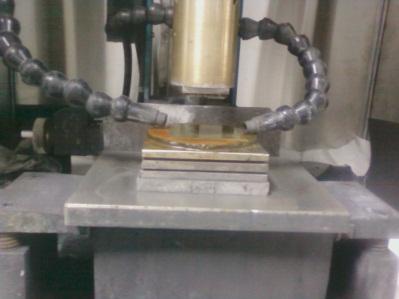
9 Tetra Methyl Amonium Hydroxide (TMAH)


 silicon surface at 80 0 C in (a)")
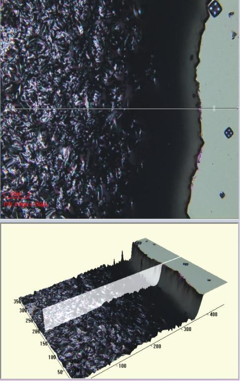
10 Micromachining of Si(100) Boiling point of KOH solution with varying concentration Etching rate of (100) silicon with varying KOH concentration and temperatures AFM scan of the etched (100) silicon surface at 80 0 C in (a) 10% wt KOH and (b) 20% wt KOH

11 Convex and Concave


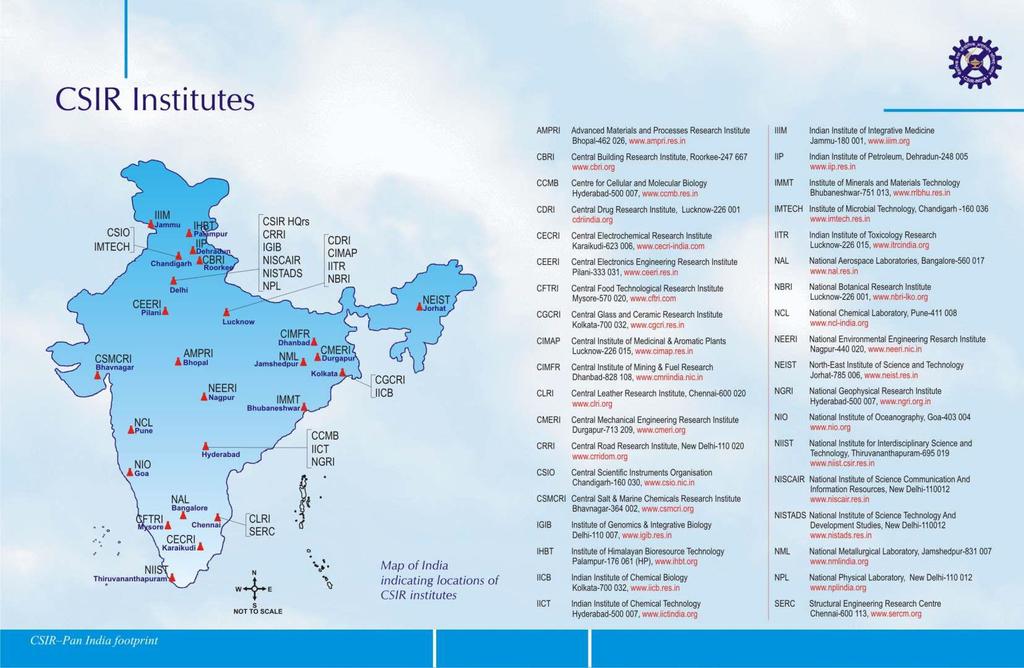
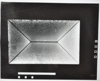
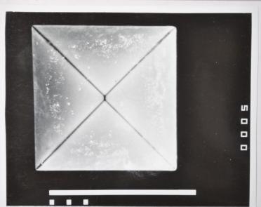
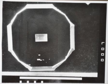
12 Alignment with crystal planes Square size 800 µm Inner Sq. size 80 µm Inner rec. size 80 and 160 µm After Etch: 776 µm and 91 µm 793 µm and 84 µm 800 and µms
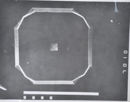
13 Bulk micromachined pressure sensor


14 Output Voltage (mv) Output Voltage (mv) Polysilicon piezoresistive pressure sensor Volts Volts Differential Pressure (bar) Differential Pressure (bar)
15 Non-conventional machining Ultrasonic Milling Electro Discharge Machining Electro-Chemical Etching Laser machining FIB etching RIE/DRIE
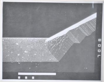
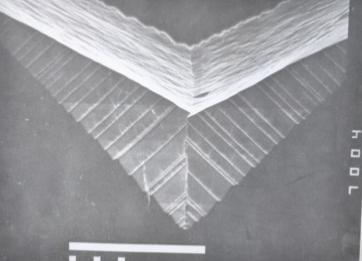
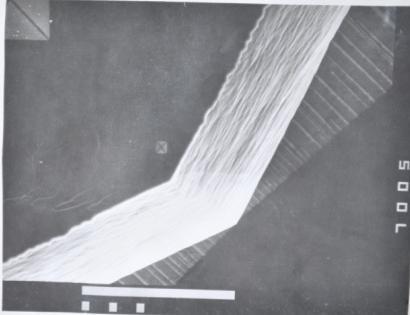
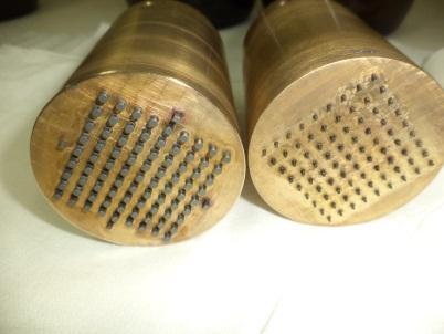
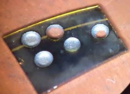
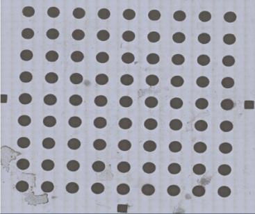
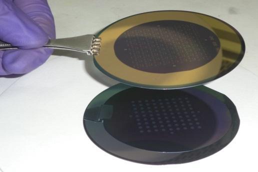
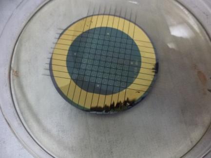
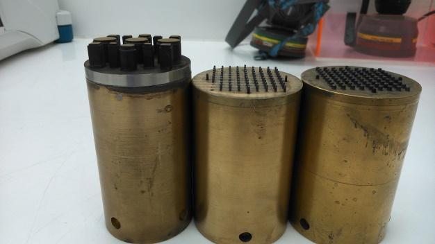
16 Integration of USM with MEMS Arrays of tool Alignment marks Silicon wafer compatibility Process sequence optimization Steep edges of the cavity Arrays of 3-D structures Any shape Economic in time Non toxic Integration with Microelectronics and MEMS processes


17 To Investigate/optimize Energy distribution from one to many tools Control of roughness Control over sharp geometries

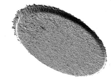
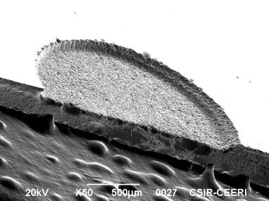
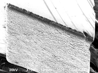
18 USM- an overview, effort made for micromachining in pressure sensor Main component of USM consists of power supply, amplitude maintainer, horn, cutting tools, slurry hose and recirculation pump. USM principle states that a power supply that generates a 20 KHz signal when applied to piezoelectric transducer, converts high frequency electrical signal into mechanical motion. This mechanical motion from the converter is amplified using amplifier maintainer and transmitted to horn. Then it causes horn and milling tool vibrated perpendicularly to the wafer face 20,000 times per second. A recirculation pump forces slurry of abrasive material boron carbide between the tool face and work piece where flow speed of slurry can be controlled by slurry hose switch. The abrasive particles propelled by the tool strike the work piece at 150,000 times at their own weight. In this way USM etch the surface of the material as per applied tip.
19 USM Etching rates for pyrex, Quartz, Silicon, Ceramic and SiC
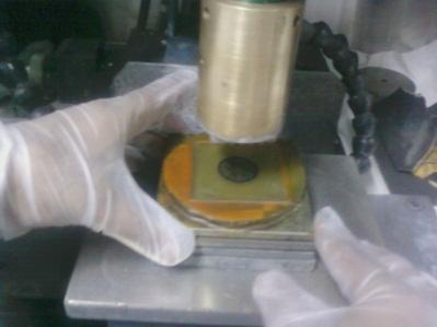
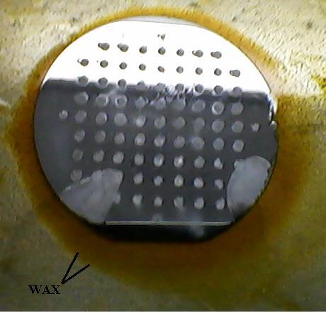
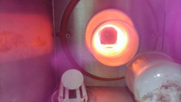
20 Pyrex Category Time (sec) Thickness (um) Etching rate(um/sec) Continuous Time Discrete Time (time not sure) (seethrough hole); and breakage
21 quartz Category Time (sec) Thickness (um) Etching rate (um/sec) Continuo us Time Discrete Time (seethrough hole)
22 Silicon Category Time (sec) Thickness (um) Etching rate(um/sec) Continuous Time (thr oughout ) 15.76
23 Ceramics Category Time (in sec) Thickness (in um) Etching rate(um/sec) Continuo us Time Discrete Time (seethrough hole)
24 Simulation results Angle Maximum Stress(*10 5 N/m 2 ) Alumina Silicon carbide Silicon Quartz Sapphire
25
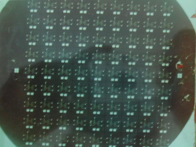
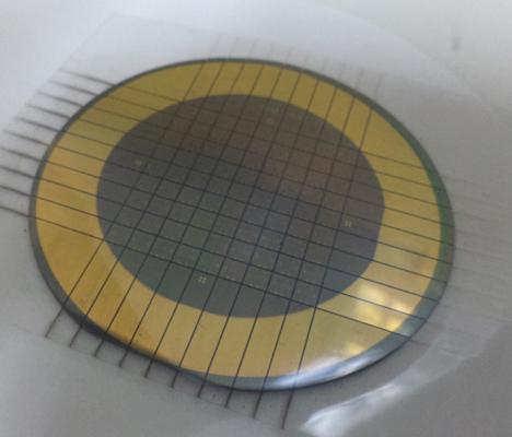
26 Surface analysis of Materials Category Surface Roughness(nm) Surface of Inside hole(um) quartz silicon Pyrex ceramics
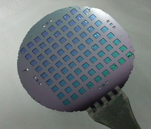
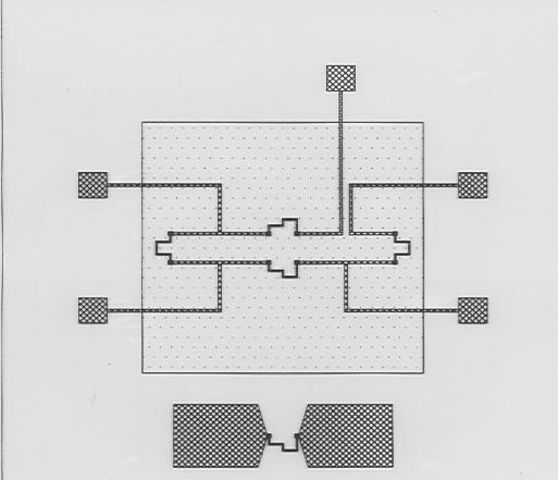
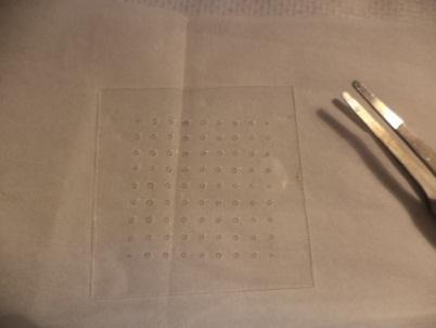
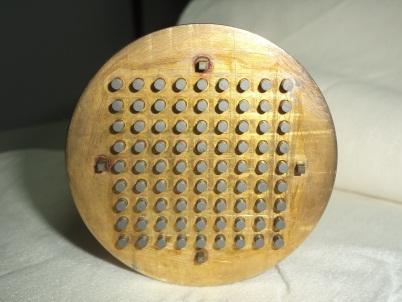
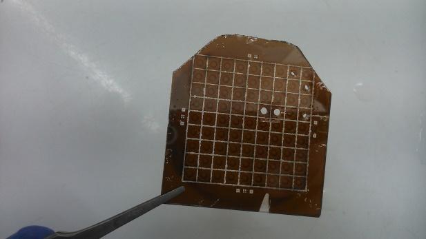
27 Schematics of circular diaphragm pressure sensor chip Resistance line length um Resistance width - 10 um Metal line width - 20 um Center resistance - 90 um away from the center Edge resistance um from the edge Contact pad um X 200 um Contact pad location um away from the diaphragm Chip size - 4mm X 4mm


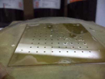

28

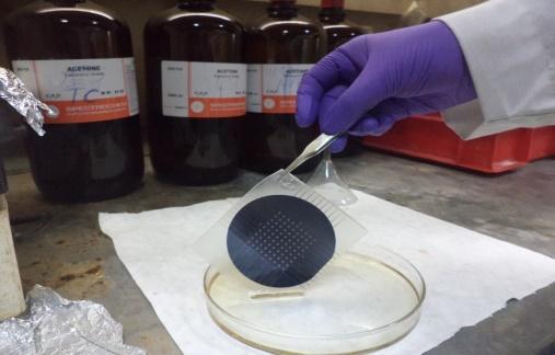
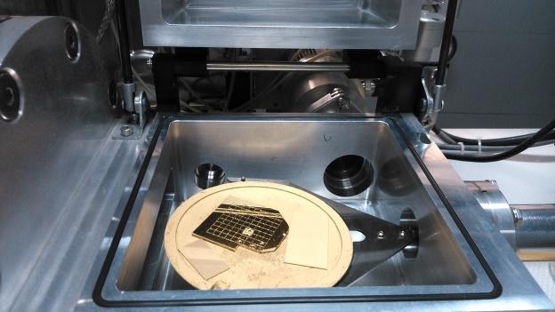
.")
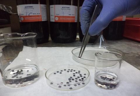
29 Cleaning process I. Degreasing : Trichloro ethylene Acetone Methanol II. Piranha: Different ratios of H 2 SO 4 and H 2 O 2 as per cleaning requirement (3:1, 5:1, 7:1). Dilute HF ( HF: DI H 2 O = 1:50) to remove the thin oxide layer.

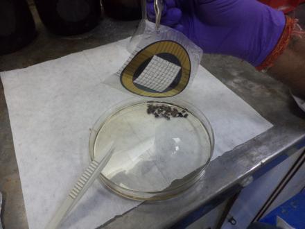
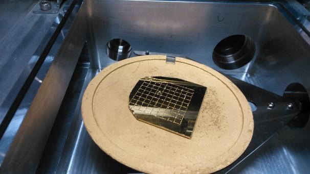
30 Work piece preparation of USM

 Surface")
 1.")
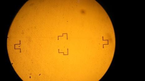
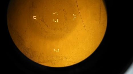
31 Post cleaning of USM process wafer and result Sample Step thickness (µm) Surface roughness (µm) Pyrex 1000 (587) 1.2 Silicon 380 (344) 1-2

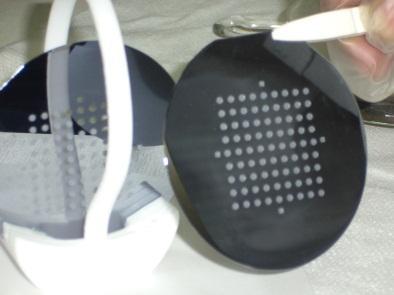
32 Hole making by DRIE

33 Principle of piezoresistive pressure sensors When applied pressure from top towards the surface of the device, where diaphragm deforms under applied pressure, the thickness of the silicon diaphragm usually strain to a few micrometers. Above the diaphragm, we placed piezoresistors (polysilicon) in the form of Wheatstone bridge, where these piezoresistors convert the stresses induced in the silicon diaphragm by applied pressure into a change in electrical resistance, which is then converted into output voltage by Wheatstone bridge circuit as shown in given figure b. We get the output voltage by equation V R R 2 4 out V in R R R R Fig a Fig b


34 Poly-Si Si Substrate 1. Silicon Substrate 4. LPCVD/EBPVD Poly-Si deposition SiO₂ Layer 2. Thermally Grown of SiO₂ Alignment mask 3. Cavity formation by ultrasonic milling 6. Ti/Au metalization


35 Control pads 7. Metal line formation in wheat stone bridge configuration 7. PECVD SiO2 passivation and Pad opining

36 Fabrication process of pressure sensor


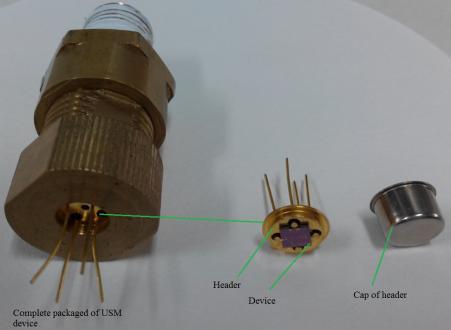
37 Processed wafer USM based diaphragm Metal line formed Poly silicon resister formed View of single pressure sensor device


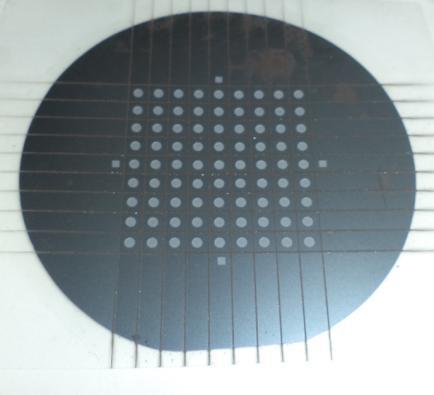

38 USM based circular diaphragm silicon pressure sensor


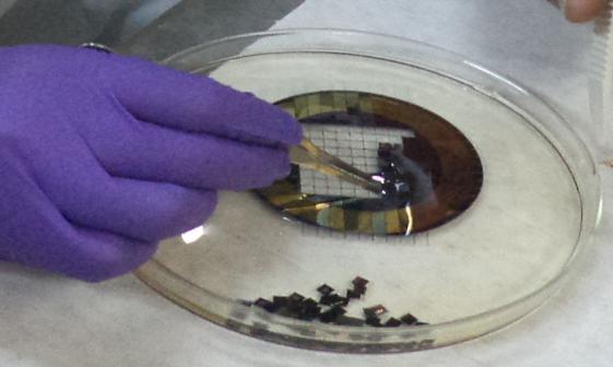
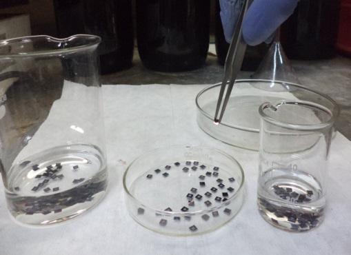
39 Typical glimpses of USM based fabrication process & measured characteristics


40 Typical glimpse of Quartz Pressure Sensor Process
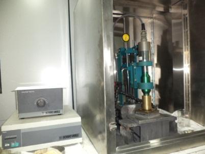
41 Manufacturers SONIC-MILL, USA for USM Mikro Tool, Singapore for Micro-EDM
42 Acknowledgments Kulwant Singh ; Ph.D Student (NIT Calicut) Rajesh Saha; Project Fellow ( Left for M.Tech) Ayon Roychaudhuri ; Ph.D Student (AcSIR) Himani Sharma; Ph.D Student (Banasthali) Pradeep Kumar; Project Fellow Director CSIR-CEERI

43 THANK YOU
Surface micromachining and Process flow part 1
 Surface micromachining and Process flow part 1 Identify the basic steps of a generic surface micromachining process Identify the critical requirements needed to create a MEMS using surface micromachining
Advanced Manufacturing Choices
 Advanced Manufacturing Choices Table of Content Mechanical Removing Techniques Ultrasonic Machining (USM) Sputtering and Focused Ion Beam Milling (FIB) Ultrasonic Machining In ultrasonic machining (USM),
There are basically two approaches for bulk micromachining of. silicon, wet and dry. Wet bulk micromachining is usually carried out
 57 Chapter 3 Fabrication of Accelerometer 3.1 Introduction There are basically two approaches for bulk micromachining of silicon, wet and dry. Wet bulk micromachining is usually carried out using anisotropic
Modeling the Fabrication Process Flow of MOS Gas Sensor based on Surface Micro-machining Technology
 Modeling the Fabrication Process Flow of MOS Gas Sensor based on Surface Micro-machining Technology Preeti Sikarwar 1, Shivani Saxena 2 1 (Student of M.Tech (VLSI), Department of Electronics Engineering,
Bulk Silicon Micromachining
 Bulk Silicon Micromachining Micro Actuators, Sensors, Systems Group University of Illinois at Urbana-Champaign Outline Types of bulk micromachining silicon anisotropic etching crystal orientation isotropic
Dr. Lynn Fuller Webpage:
 ROCHESTER INSTITUTE OF TECHNOLOGY MICROELECTRONIC ENGINEERING Microelectromechanical Systems (MEMs) Process Integration Dr. Lynn Fuller Webpage: http://people.rit.edu/lffeee 82 Lomb Memorial Drive Rochester,
Manufacturing Technologies for MEMS and SMART SENSORS
 4 Manufacturing Technologies for MEMS and SMART SENSORS Dr. H. K. Verma Distinguished Professor (EEE) Sharda University, Greater Noida (Formerly: Deputy Director and Professor of Instrumentation Indian
L5: Micromachining processes 1/7 01/22/02
 97.577 L5: Micromachining processes 1/7 01/22/02 5: Micromachining technology Top-down approaches to building large (relative to an atom or even a transistor) structures. 5.1 Bulk Micromachining A bulk
Lecture 5. SOI Micromachining. SOI MUMPs. SOI Micromachining. Silicon-on-Insulator Microstructures. Agenda:
 EEL6935 Advanced MEMS (Spring 2005) Instructor: Dr. Huikai Xie SOI Micromachining Agenda: SOI Micromachining SOI MUMPs Multi-level structures Lecture 5 Silicon-on-Insulator Microstructures Single-crystal
Micromachining AMT 2505
 Micromachining AMT 2505 Shanmuga Raja.B (BVB0912004) Module leader : Mr. Raja Hussain Introduction Micromachining are inherently connected to the evolution of Micro Electro Mechanical Systems (MEMS). Decades
Lecture 7 CMOS MEMS. CMOS MEMS Processes. CMOS MEMS Processes. Why CMOS-MEMS? Agenda: CMOS MEMS: Fabrication. MEMS structures can be made
 EEL6935 Advanced MEMS (Spring 2005) Instructor: Dr. Huikai Xie CMOS MEMS Agenda: Lecture 7 CMOS MEMS: Fabrication Pre-CMOS Intra-CMOS Post-CMOS Deposition Etching Why CMOS-MEMS? Smart on-chip CMOS circuitry
Silicon Microparticle Ejection Using Mist-jet Technology
 Yokoyama et al.: Silicon Microparticle Ejection Using Mist-jet Technology (1/5) [Technical Paper] Silicon Microparticle Ejection Using Mist-jet Technology Yoshinori Yokoyama*, Takaaki Murakami*, Takashi
Chapter 2 OVERVIEW OF MEMS
 6 Chapter 2 OVERVIEW OF MEMS 2.1 MEMS and Microsystems The term MEMS is an abbreviation of microelectromechanical system. MEMS contains components ofsizes in 1 micrometer to 1 millimeter. The core element
5.8 Diaphragm Uniaxial Optical Accelerometer
 5.8 Diaphragm Uniaxial Optical Accelerometer Optical accelerometers are based on the BESOI (Bond and Etch back Silicon On Insulator) wafers, supplied by Shin-Etsu with (100) orientation, 4 diameter and
Micro-Electro-Mechanical Systems (MEMS) Fabrication. Special Process Modules for MEMS. Principle of Sensing and Actuation
 Fabrication. Special Process Modules for MEMS. Principle of Sensing and Actuation") Micro-Electro-Mechanical Systems (MEMS) Fabrication Fabrication Considerations Stress-Strain, Thin-film Stress, Stiction Special Process Modules for MEMS Bonding, Cavity Sealing, Deep RIE, Spatial forming
Micro-Electro-Mechanical Systems (MEMS) Fabrication Fabrication Considerations Stress-Strain, Thin-film Stress, Stiction Special Process Modules for MEMS Bonding, Cavity Sealing, Deep RIE, Spatial forming
General Introduction to Microstructure Technology p. 1 What is Microstructure Technology? p. 1 From Microstructure Technology to Microsystems
 General Introduction to Microstructure Technology p. 1 What is Microstructure Technology? p. 1 From Microstructure Technology to Microsystems Technology p. 9 The Parallels to Microelectronics p. 15 The
Micro-Electro-Mechanical Systems (MEMS) Fabrication. Special Process Modules for MEMS. Principle of Sensing and Actuation
 Fabrication. Special Process Modules for MEMS. Principle of Sensing and Actuation") Micro-Electro-Mechanical Systems (MEMS) Fabrication Fabrication Considerations Stress-Strain, Thin-film Stress, Stiction Special Process Modules for MEMS Bonding, Cavity Sealing, Deep RIE, Spatial forming
Micro-Electro-Mechanical Systems (MEMS) Fabrication Fabrication Considerations Stress-Strain, Thin-film Stress, Stiction Special Process Modules for MEMS Bonding, Cavity Sealing, Deep RIE, Spatial forming
EE 330 Lecture 9. IC Fabrication Technology Part 2
 EE 330 Lecture 9 IC Fabrication Technology Part 2 Quiz 8 A 2m silicon crystal is cut into wafers using a wire saw. If the wire diameter is 220um and the wafer thickness is 350um, how many wafers will this
Welcome MNT Conference 1 Albuquerque, NM - May 2010
 Welcome MNT Conference 1 Albuquerque, NM - May 2010 Introduction to Design Outline What is MEMs Design General Considerations Application Packaging Process Flow What s available Sandia SUMMiT Overview
Oil-filled isolated high pressure sensor for high temperature application
 Oil-filled isolated high pressure sensor for high temperature application Zhuangde Jiang,, Libo Zhao, Yulong Zhao, Yuanhao Liu, Philip D. Prewett, Kyle Jiang State Key Laboratory for Manufacturing Systems
Micro-Electro-Mechanical Systems (MEMS) Fabrication. Special Process Modules for MEMS. Principle of Sensing and Actuation
 Fabrication. Special Process Modules for MEMS. Principle of Sensing and Actuation") Micro-Electro-Mechanical Systems (MEMS) Fabrication Fabrication Considerations Stress-Strain, Thin-film Stress, Stiction Special Process Modules for MEMS Bonding, Cavity Sealing, Deep RIE, Spatial forming
Micro-Electro-Mechanical Systems (MEMS) Fabrication Fabrication Considerations Stress-Strain, Thin-film Stress, Stiction Special Process Modules for MEMS Bonding, Cavity Sealing, Deep RIE, Spatial forming
Available online at ScienceDirect. Procedia Materials Science 10 (2015 )
") Available online at www.sciencedirect.com ScienceDirect Procedia Materials Science 10 (2015 ) 254 262 2nd International Conference on Nanomaterials and Technologies (CNT 2014) Enhancing the Performance
Available online at www.sciencedirect.com ScienceDirect Procedia Materials Science 10 (2015 ) 254 262 2nd International Conference on Nanomaterials and Technologies (CNT 2014) Enhancing the Performance
An optimization study on the anisotropic TMAH wet etching of silicon (100)
") International Journal of Material Science Innovations (IJMSI) 1 (3): 115-123, 2013 ISSN: 2289-4063 Academic Research Online Publisher Research Article An optimization study on the anisotropic TMAH wet
International Journal of Material Science Innovations (IJMSI) 1 (3): 115-123, 2013 ISSN: 2289-4063 Academic Research Online Publisher Research Article An optimization study on the anisotropic TMAH wet
Why Probes Look the Way They Do Concepts and Technologies of AFM Probes Manufacturing
 Agilent Technologies AFM e-seminar: Understanding and Choosing the Correct Cantilever for Your Application Oliver Krause NanoWorld Services GmbH All mentioned company names and trademarks are property
Lecture 5: Micromachining
 MEMS: Fabrication Lecture 5: Micromachining Prasanna S. Gandhi Assistant Professor, Department of Mechanical Engineering, Indian Institute of Technology, Bombay, Recap: Last Class E-beam lithography X-ray
ME 189 Microsystems Design and Manufacture. Chapter 9. Micromanufacturing
 ME 189 Microsystems Design and Manufacture Chapter 9 Micromanufacturing This chapter will offer an overview of the application of the various fabrication techniques described in Chapter 8 in the manufacturing
EE 330 Lecture 9. IC Fabrication Technology Part II. -Oxidation -Epitaxy -Polysilicon -Planarization -Resistance and Capacitance in Interconnects
 EE 330 Lecture 9 IC Fabrication Technology Part II -Oxidation -Epitaxy -Polysilicon -Planarization -Resistance and Capacitance in Interconnects Review from Last Time IC Fabrication Technology Crystal Preparation
MEMS Fabrication. Beyond Integrated Circuits. MEMS Basic Concepts
 MEMS Fabrication Beyond Integrated Circuits MEMS Basic Concepts Uses integrated circuit fabrication techniques to make mechanical as well as electrical components on a single chip. Small size 1µm 1mm Typically
Surface Micromachining
 Surface Micromachining Outline Introduction Material often used in surface micromachining Material selection criteria in surface micromachining Case study: Fabrication of electrostatic motor Major issues
Today s Class. Materials for MEMS
 Lecture 2: VLSI-based Fabrication for MEMS: Fundamentals Prasanna S. Gandhi Assistant Professor, Department of Mechanical Engineering, Indian Institute of Technology, Bombay, Recap: Last Class What is
Microstructures using RF sputtered PSG film as a sacrificial layer in surface micromachining
 Sādhanā Vol. 34, Part 4, August 2009, pp. 557 562. Printed in India Microstructures using RF sputtered PSG film as a sacrificial layer in surface micromachining VIVEKANAND BHATT 1,, SUDHIR CHANDRA 1 and
EE C245 ME C218 Introduction to MEMS Design Fall 2007
 EE C245 ME C218 Introduction to MEMS Design Fall 2007 Prof. Clark T.-C. Nguyen Dept. of Electrical Engineering & Computer Sciences University of California at Berkeley Berkeley, CA 94720 Lecture 10: Bulk
Surface Micromachining
 Surface Micromachining Micro Actuators, Sensors, Systems Group University of Illinois at Urbana-Champaign Outline Definition of surface micromachining Most common surface micromachining materials - polysilicon
6.777J/2.732J Design and Fabrication of Microelectromechanical Devices Spring Term Solution to Problem Set 2 (16 pts)
") 6.777J/2.732J Design and Fabrication of Microelectromechanical Devices Spring Term 2007 By Brian Taff (Adapted from work by Feras Eid) Solution to Problem Set 2 (16 pts) Issued: Lecture 4 Due: Lecture
6.777J/2.732J Design and Fabrication of Microelectromechanical Devices Spring Term 2007 By Brian Taff (Adapted from work by Feras Eid) Solution to Problem Set 2 (16 pts) Issued: Lecture 4 Due: Lecture
DESIGN OF BOSSED SILICON MEMBRANES FOR HIGH SENSITIVITY MICROPHONE APPLICATIONS
 Stresa, Italy, 26-28 April 2006 DESIGN OF BOSSED SILICON MEMBRANES FOR HIGH SENSITIVITY MICROPHONE APPLICATIONS P. Martins 1, S.Beclin 2, S.Brida 2, S.Metivet 2, O.Stojanovic 2, C. Malhaire 1 1: LPM, UMR
Etching Mask Properties of Diamond-Like Carbon Films
 N. New Nawachi Diamond et al. and Frontier Carbon Technology 13 Vol. 15, No. 1 2005 MYU Tokyo NDFCT 470 Etching Mask Properties of Diamond-Like Carbon Films Norio Nawachi *, Akira Yamamoto, Takahiro Tsutsumoto
Semiconductor Manufacturing Process 10/11/2005
 Semiconductor Manufacturing Process 10/11/2005 Photolithography Oxidation CVD PVD Photolithography The purpose of photolithography is to imprint the desired pattern of a micro component on a substrate,
UNCONVENTIONAL MACHINING PROCESS UNIT 1 INTRODUCTION. Prepared by S. SENTHIL KUMAR AP / MECH SVCET
 UNCONVENTIONAL MACHINING PROCESS UNIT 1 INTRODUCTION Prepared by S. SENTHIL KUMAR AP / MECH SVCET INTRODUCTION Conventional machining process Metal is removed by means of tool which is harder than work
Atomic Layer Deposition(ALD)
") Atomic Layer Deposition(ALD) AlO x for diffusion barriers OLED displays http://en.wikipedia.org/wiki/atomic_layer_deposition#/media/file:ald_schematics.jpg Lam s market-leading ALTUS systems combine CVD
Atomic Layer Deposition(ALD) AlO x for diffusion barriers OLED displays http://en.wikipedia.org/wiki/atomic_layer_deposition#/media/file:ald_schematics.jpg Lam s market-leading ALTUS systems combine CVD
Gaetano L Episcopo. Introduction to MEMS
 Gaetano L Episcopo Introduction to MEMS What are MEMS? Micro Electro Mechanichal Systems MEMS are integrated devices, or systems of devices, with microscopic parts, such as: Mechanical Parts Electrical
Preface Preface to First Edition
 Contents Foreword Preface Preface to First Edition xiii xv xix CHAPTER 1 MEMS: A Technology from Lilliput 1 The Promise of Technology 1 What Are MEMS or MST? 2 What Is Micromachining? 3 Applications and
Chemical Vapor Deposition
 Chemical Vapor Deposition ESS4810 Lecture Fall 2010 Introduction Chemical vapor deposition (CVD) forms thin films on the surface of a substrate by thermal decomposition and/or reaction of gas compounds
Micro-Scale Engineering I Microelectromechanical Systems (MEMS) Y. C. Lee
 Y. C. Lee") Micro-Scale Engineering I Microelectromechanical Systems (MEMS) Y. C. Lee Department of Mechanical Engineering University of Colorado Boulder, CO 80309-0427 leeyc@colorado.edu September 2, 2008 1 Three
Micro-Scale Engineering I Microelectromechanical Systems (MEMS) Y. C. Lee Department of Mechanical Engineering University of Colorado Boulder, CO 80309-0427 leeyc@colorado.edu September 2, 2008 1 Three
Isolation Technology. Dr. Lynn Fuller
 ROCHESTER INSTITUTE OF TECHNOLOGY MICROELECTRONIC ENGINEERING Isolation Technology Dr. Lynn Fuller Motorola Professor 82 Lomb Memorial Drive Rochester, NY 14623-5604 Tel (585) 475-2035 Fax (585) 475-5041
Lecture 10: MultiUser MEMS Process (MUMPS)
") MEMS: Fabrication Lecture 10: MultiUser MEMS Process (MUMPS) Prasanna S. Gandhi Assistant Professor, Department of Mechanical Engineering, Indian Institute of Technology, Bombay, 1 Recap Various VLSI based
MEMS: Fabrication Lecture 10: MultiUser MEMS Process (MUMPS) Prasanna S. Gandhi Assistant Professor, Department of Mechanical Engineering, Indian Institute of Technology, Bombay, 1 Recap Various VLSI based
Surface Micromachining Process for the Integration of AlN Piezoelectric Microstructures
 Surface Micromachining Process for the Integration of AlN Piezoelectric Microstructures Saravanan. S, Erwin Berenschot, Gijs Krijnen and Miko Elwenspoek Transducers Science and Technology Laboratory University
Silicon Wafer Processing PAKAGING AND TEST
 Silicon Wafer Processing PAKAGING AND TEST Parametrical test using test structures regularly distributed in the wafer Wafer die test marking defective dies dies separation die fixing (not marked as defective)
Microelectronics. Integrated circuits. Introduction to the IC technology M.Rencz 11 September, Expected decrease in line width
 Microelectronics Introduction to the IC technology M.Rencz 11 September, 2002 9/16/02 1/37 Integrated circuits Development is controlled by the roadmaps. Self-fulfilling predictions for the tendencies
Experimental Study of Chemical Etching on EN8 & EN38
 Journal for Research Volume 03 Issue 01 March 2017 ISSN: 2395-7549 Experimental Study of Chemical Etching on EN8 & EN38 Nirpakash Uppal Assistant Professor Department of Mechanical Engineering G.G.S.C.M.T
A Functional Micro-Solid Oxide Fuel Cell with. Nanometer Freestanding Electrolyte
 Electronic Supplementary Material (ESI) for Journal of Materials Chemistry A. This journal is The Royal Society of Chemistry 2017 SUPPLEMENTARY INFORMATION A Functional Micro-Solid Oxide Fuel Cell with
A diffused silicon pressure transducer with stress concentrated at transverse gages. Technical paper 267
 A diffused silicon pressure transducer with stress concentrated at transverse gages Technical paper 267 A diffused silicon pressure transducer with stress concentrated at transverse gages Many Meggitt
EE C245 ME C218 Introduction to MEMS Design Fall 2011
 Lecture Outline EE C245 ME C218 Introduction to MEMS Design Fall 2011 Prof. Clark T.-C. Nguyen Dept. of Electrical Engineering & Computer Sciences University of California at Berkeley Berkeley, CA 94720
PRESSURE SENSOR MODEL ACTIVITY. Pressure Sensor Model Activity
 PRESSURE SENSOR MODEL ACTIVITY Pressure Sensor Model Activity Unit Overview This activity uses household materials to build a pressure sensor Wheatstone Bridge sensing circuit Flexible diaphragm Reference
Fabrication Technology, Part II
 EEL5225: Principles of MEMS Transducers (Fall 2003) Fabrication Technology, Part II Agenda: Process Examples TI Micromirror fabrication process SCREAM CMOS-MEMS processes Wafer Bonding LIGA Reading: Senturia,
Chapter 4 Fabrication Process of Silicon Carrier and. Gold-Gold Thermocompression Bonding
 Chapter 4 Fabrication Process of Silicon Carrier and Gold-Gold Thermocompression Bonding 4.1 Introduction As mentioned in chapter 2, the MEMs carrier is designed to integrate the micro-machined inductor
MEMS II: January 23. Lab 1: Pop-up mirror - PolyMUMPS - Thermal actuators - Mirror CoventorWare
 MEMS II: January 23 Lab 1: Pop-up mirror - PolyMUMPS - Thermal actuators - Mirror CoventorWare Microelectromechanical Systems (MEMS) Multi-User MEMS Processes (MUMPS) Example Design Anchor hole 2.0 0.5
MEMS prototyping using RF sputtered films
 Indian Journal of Pure & Applied Physics Vol. 45, April 2007, pp. 326-331 MEMS prototyping using RF sputtered films Sudhir Chandra, Vivekanand Bhatt, Ravindra Singh, Preeti Sharma & Prem Pal* Centre for
Mikrosensorer. Microfabrication 1
 Mikrosensorer Microfabrication 1 Literature Introductory MEMS Fabrication and Applications Thomas M. Adams and Richard A. Layton Available as ebook on http://www.lub.lu.se/en/search/lubsearch.html This
Poly-SiGe MEMS actuators for adaptive optics
 Poly-SiGe MEMS actuators for adaptive optics Blake C.-Y. Lin a,b, Tsu-Jae King a, and Richard S. Muller a,b a Department of Electrical Engineering and Computer Sciences, b Berkeley Sensor and Actuator
MICROULTRASONIC MACHINING USING MULTITOOLS
 MICROULTRASONIC MACHINING USING MULTITOOLS EGASHIRA Kai, TANIGUCHI Tomoya, TSUCHIYA Hachiro and MIYAZAKI Makoto Kyoto Institute of Technology, Kyoto 606-8585, Japan Abstract Multitools have been fabricated
HOMEWORK 4 and 5. March 15, Homework is due on Monday March 30, 2009 in Class. Answer the following questions from the Course Textbook:
 HOMEWORK 4 and 5 March 15, 2009 Homework is due on Monday March 30, 2009 in Class. Chapter 7 Answer the following questions from the Course Textbook: 7.2, 7.3, 7.4, 7.5, 7.6*, 7.7, 7.9*, 7.10*, 7.16, 7.17*,
Change in stoichiometry
 Measurement of Gas Sensor Performance Gas sensing materials: 1. Sputtered ZnO film (150 nm (Massachusetts Institute of Technology) 2. Sputtered SnO 2 film (60 nm) (Fraunhofer Institute of Physical Measurement
Microfabrication of Heterogeneous, Optimized Compliant Mechanisms SUNFEST 2001 Luo Chen Advisor: Professor G.K. Ananthasuresh
 Microfabrication of Heterogeneous, Optimized Compliant Mechanisms SUNFEST 2001 Luo Chen Advisor: Professor G.K. Ananthasuresh Fig. 1. Single-material Heatuator with selective doping on one arm (G.K. Ananthasuresh)
Applications of High-Performance MEMS Pressure Sensors Based on Dissolved Wafer Process
 Applications of High-Performance MEMS Pressure Sensors Based on Dissolved Wafer Process Srinivas Tadigadapa and Sonbol Massoud-Ansari Integrated Sensing Systems (ISSYS) Inc., 387 Airport Industrial Drive,
Passive TCF Compensation in High Q Silicon Micromechanical Resonators
 Passive TCF Compensation in High Q Silicon Micromechanical Resonators A.K. Samarao, G. Casinovi and F. Ayazi IEEE International Conference on Micro Electro Mechanical Systems pp. 116 119, January 2010
MICRO-ELECTRO-MECHANICAL VARIABLE BLAZE GRATINGS
 MICRO-ELECTRO-MECHANICAL VARIABLE BLAZE GRATINGS D. M. Burns and V. M. Bright Air Force Institute of Technology Department of Electrical and Computer Engineering Wright-Patterson Air Force Base, OH 45433-7765
Equipment and Process Challenges for the Advanced Packaging Landscape
 Equipment and Process Challenges for the Advanced Packaging Landscape Veeco Precision Surface Processing Laura Mauer June 2018 1 Copyright 2018 Veeco Instruments Inc. Outline» Advanced Packaging Market
Solid State Sensors. Microfabrication 8/22/08 and 8/25/08
 Solid State Sensors Microfabrication 8/22/08 and 8/25/08 Purpose of This Material To introduce the student to microfabrication techniques as used to fabricate MEMS Sensors Understand concepts not specifics
EECS130 Integrated Circuit Devices
 EECS130 Integrated Circuit Devices Professor Ali Javey 9/13/2007 Fabrication Technology Lecture 1 Silicon Device Fabrication Technology Over 10 15 transistors (or 100,000 for every person in the world)
A High Speed Surface Illuminated Si Photodiode. Using Microstructured Holes for Absorption. Enhancements at nm wavelength
 A High Speed Surface Illuminated Si Photodiode Using Microstructured Holes for Absorption Enhancements at 900 1000 nm wavelength Supporting Information Yang Gao, Hilal Cansizoglu, Soroush Ghandiparsi,
Czochralski Crystal Growth
 Czochralski Crystal Growth Crystal Pulling Crystal Ingots Shaping and Polishing 300 mm wafer 1 2 Advantage of larger diameter wafers Wafer area larger Chip area larger 3 4 Large-Diameter Wafer Handling
OPTIMAL SELECTION OF PROCESS PARAMETERS OF ULTRASONIC MACHINING (USM) SYSTEM
 SYSTEM") OPTIMAL SELECTION OF PROCESS PARAMETERS OF ULTRASONIC MACHINING (USM) SYSTEM BY H. L A L C H H U A N V E L A B.E. (Mech), MNNIT, Allahabad (Formerly M.N.R.E.C., Allahabad), 1987; M.Tech. (Mech), IT-BHU,
OPTIMAL SELECTION OF PROCESS PARAMETERS OF ULTRASONIC MACHINING (USM) SYSTEM BY H. L A L C H H U A N V E L A B.E. (Mech), MNNIT, Allahabad (Formerly M.N.R.E.C., Allahabad), 1987; M.Tech. (Mech), IT-BHU,
SOI PIEZORESISTIVE LOW PRESSURE SENSOR FOR HIGH TEMPERATURE ENVIRONMENTS
 SOI PIEZORESISTIVE LOW PRESSURE SENSOR FOR HIGH TEMPERATURE ENVIRONMENTS MILČE M. SMILJANIĆ KATARINA RADULOVIĆ ŽARKO LAZIĆ VESNA JOVIĆ BOGDAN POPOVIĆ Institute of Chemistry, Technology and Metallurgy-Centre
CHARACTERIZATION OF ELECTROTHERMAL ACTUATORS AND ARRAYS FABRICATED IN A FOUR-LEVEL, PLANARIZED SURFACE-MICROMACHINED POLYCRYSTALLINE SILICON PROCESS
 CHARACTERIZATION OF ELECTROTHERMAL ACTUATORS AND ARRAYS FABRICATED IN A FOUR-LEVEL, PLANARIZED SURFACE-MICROMACHINED POLYCRYSTALLINE SILICON PROCESS John H. Comtois*, M. Adrian Michalicek*, and Carole
CMOS Technology. Flow varies with process types & company. Start with substrate selection. N-Well CMOS Twin-Well CMOS STI
 CMOS Technology Flow varies with process types & company N-Well CMOS Twin-Well CMOS STI Start with substrate selection Type: n or p Doping level, resistivity Orientation, 100, or 101, etc Other parameters
A novel measuring system for the metrological characterization of piezoresistive films at high temperature
 P1.1 A novel measuring system for the metrological characterization of piezoresistive films at high temperature Damiano Crescini, and Marco Romani Dipartimento di Elettronica per l'automazione Facoltà
United States. Patent (19)
") United States. Patent (19) Aagard 54 PIEZORESISTIVE PRESSURE SENSOR 75 Inventor: Roger L. Aagard, Prior Lake, Minn. 73) Assignee: Honeywell Inc., Minneapolis, Minn. 21 Appl. No.: 774,127 22 Filed: Sep.
United States. Patent (19) Aagard 54 PIEZORESISTIVE PRESSURE SENSOR 75 Inventor: Roger L. Aagard, Prior Lake, Minn. 73) Assignee: Honeywell Inc., Minneapolis, Minn. 21 Appl. No.: 774,127 22 Filed: Sep.
Supporting Information
 Supporting Information Fast-Response, Sensitivitive and Low-Powered Chemosensors by Fusing Nanostructured Porous Thin Film and IDEs-Microheater Chip Zhengfei Dai,, Lei Xu,#,, Guotao Duan *,, Tie Li *,,
PHYS 534 (Fall 2008) Process Integration OUTLINE. Examples of PROCESS FLOW SEQUENCES. >Surface-Micromachined Beam
 Process Integration OUTLINE. Examples of PROCESS FLOW SEQUENCES. >Surface-Micromachined Beam") PHYS 534 (Fall 2008) Process Integration Srikar Vengallatore, McGill University 1 OUTLINE Examples of PROCESS FLOW SEQUENCES >Semiconductor diode >Surface-Micromachined Beam Critical Issues in Process
PHYS 534 (Fall 2008) Process Integration Srikar Vengallatore, McGill University 1 OUTLINE Examples of PROCESS FLOW SEQUENCES >Semiconductor diode >Surface-Micromachined Beam Critical Issues in Process
A Computational Approach for Simulating P-type Silicon Piezoresistor Using Four Point Bending Setup
 A Computational Approach for Simulating P-type Silicon Piezoresistor Using Four Point Bending Setup Authors: T. H. Tan 1, S.J.N Mitchell 1, D.W. McNeill 1, H. Wadsworth 2, S. Strahan 2. 1 School of Electronics,
A Nano-thick SOI Fabrication Method
 A Nano-thick SOI Fabrication Method C.-H. Huang 1, J.T. Cheng 1, Y.-K. Hsu 1, C.-L. Chang 1, H.-W. Wang 1, S.-L. Lee 1,2, and T.-H. Lee 1,2 1 Dept. of Mechanical Engineering National Central University,
GAS TURBINE ENGINE PROGNOSTICS AND EQUIPMENT HEALTH MANAGEMENT
 Project Project director Research unit E-20-F75 JACOBS CEE LAURENCE Title GAS TURBINE ENGINE PROGNOSTICS AND EQUIPMENT HEALTH MANAGEMENT Project date 8/31/2001 MEMS Sensors for the Non-Contact Ultrasonic
DESIGN AND FABRICATION OF MEMS CANTILEVER AND OTHER BEAM STRUCTURES
 DESIGN AND FABRICATION OF MEMS CANTILEVER AND OTHER BEAM STRUCTURES by SHANKAR DUTTA Department of Physics Submitted in fulfillment of the requirements of the degree of Doctor of Philosophy to the INDIAN
Fabrication Technology, Part I
 EEL5225: Principles of MEMS Transducers (Fall 2003) Fabrication Technology, Part I Agenda: Oxidation, layer deposition (last lecture) Lithography Pattern Transfer (etching) Impurity Doping Reading: Senturia,
Fabrication of regular silicon microstructures by photo-electrochemical etching of silicon
 phys. stat. sol. (c) 2, No. 9, 3198 3202 (2005) / DOI 10.1002/pssc.200461110 Fabrication of regular silicon microstructures by photo-electrochemical etching of silicon G. Barillaro *, P. Bruschi, A. Diligenti,
Nontraditional Machining Processes
 Nontraditional Machining Processes The NTM processes can be divided into four basic categories: I. Chemical (Chemical reaction), II. Electrochemical (Electrolytic dissolution), III. Mechanical (Multipoint
Ion Implantation Most modern devices doped using ion implanters Ionize gas sources (single +, 2+ or 3+ ionization) Accelerate dopant ions to very
 Accelerate dopant ions to very") Ion Implantation Most modern devices doped using ion implanters Ionize gas sources (single +, 2+ or 3+ ionization) Accelerate dopant ions to very high voltages (10-600 KeV) Use analyzer to selection charge/mass
Ion Implantation Most modern devices doped using ion implanters Ionize gas sources (single +, 2+ or 3+ ionization) Accelerate dopant ions to very high voltages (10-600 KeV) Use analyzer to selection charge/mass
Lecture 22: Integrated circuit fabrication
 Lecture 22: Integrated circuit fabrication Contents 1 Introduction 1 2 Layering 4 3 Patterning 7 4 Doping 8 4.1 Thermal diffusion......................... 10 4.2 Ion implantation.........................
FABRICATION OF SWTICHES ON POLYMER-BASED BY HOT EMBOSSING. Chao-Heng Chien, Hui-Min Yu,
 Stresa, Italy, 26-28 April 2006 FABRICATION OF SWTICHES ON POLYMER-BASED BY HOT EMBOSSING, Mechanical Engineering Department, Tatung University 40 Chung Shan N. Rd. Sec. 3 Taipei, Taiwan ABSTRACT In MEMS
ULTRAPRECISION MICROMACHINING OF MICROFLUIDIC DEVICES BY USE OF A HIGH-SPEED AIRBEARING SPINDLE
 ULTRAPRECISION MICROMACHINING OF MICROFLUIDIC DEVICES BY USE OF A HIGH-SPEED AIRBEARING SPINDLE Chunhe Zhang 1, Allen Y. Yi 1, Lei Li 1, L. James Lee 1, R. Ryan Vallance 2, Eric Marsh 3 1 The Ohio State
Question Bank for Microsystems Fabrication using Advanced Machining Processes
 Question Bank for Microsystems Fabrication using Advanced Machining Processes Q1. Short answer questions 1. Draw a schematic to classify all material removal processes. 2. What is size range of a bacterial
Chapter 2. Density 2.65 g/cm 3 Melting point Young s modulus Tensile strength Thermal conductivity Dielectric constant 3.
 Chapter 2 Thin Film Materials Thin films of Silicon dioxide, Silicon nitride and Polysilicon have been utilized in the fabrication of absolute micro pressure sensor. These materials are studied and discussed
2242 ieee transactions on ultrasonics, ferroelectrics, and frequency control, vol. 52, no. 12, december 2005
 2242 ieee transactions on ultrasonics, ferroelectrics, and frequency control, vol. 52, no. 12, december 2005 Capacitive Micromachined Ultrasonic Transducers: Fabrication Technology Arif Sanlı Ergun, Member,
This Appendix discusses the main IC fabrication processes.
 IC Fabrication B B.1 Introduction This Appendix discusses the main IC fabrication processes. B.2 NMOS fabrication NMOS transistors are formed in a p-type substrate. The NMOS fabrication process requires
Mostafa Soliman, Ph.D. May 5 th 2014
 Mostafa Soliman, Ph.D. May 5 th 2014 Mostafa Soliman, Ph.D. 1 Basic MEMS Processes Front-End Processes Back-End Processes 2 Mostafa Soliman, Ph.D. Wafers Deposition Lithography Etch Chips 1- Si Substrate
Ion Implantation Most modern devices doped using ion implanters Implant dopants by accelerating individual atoms (ions) Ionize gas sources (single +,
 Ionize gas sources (single +,") Ion Implantation Most modern devices doped using ion implanters Implant dopants by accelerating individual atoms (ions) Ionize gas sources (single +, 2+ or 3+ ionization) Use analyzer to selection charge/mass
Ion Implantation Most modern devices doped using ion implanters Implant dopants by accelerating individual atoms (ions) Ionize gas sources (single +, 2+ or 3+ ionization) Use analyzer to selection charge/mass
Tensile Testing of Polycrystalline Silicon Thin Films Using Electrostatic
 Paper Tensile Testing of Polycrystalline Silicon Thin Films Using Electrostatic Force Grip Member Toshiyuki Tsuchiya (Toyota Central Labs., Inc.) Member Osamu Tabata (Ritsumeikan University) Jiro Sakata
Chapter 3 CMOS processing technology
 Chapter 3 CMOS processing technology (How to make a CMOS?) Si + impurity acceptors(p-type) donors (n-type) p-type + n-type => pn junction (I-V) 3.1.1 (Wafer) Wafer = A disk of silicon (0.25 mm - 1 mm thick),
Fairchild Semiconductor Application Note June 1983 Revised March 2003
 Fairchild Semiconductor Application Note June 1983 Revised March 2003 High-Speed CMOS (MM74HC) Processing The MM74HC logic family achieves its high speed by utilizing microcmos Technology. This is a 3.5