Surface Micromachining
|
|
|
- Maximilian Owen Jordan
- 5 years ago
- Views:
Transcription

1 Surface Micromachining Micro Actuators, Sensors, Systems Group University of Illinois at Urbana-Champaign
2 Outline Definition of surface micromachining Most common surface micromachining materials - polysilicon and silicon oxide LPCVD deposition of polysilicon, silicon nitride, and oxide plasma etching for patterning structural layer micromachined hinges - fabrication process and assembly technique micromachined dimples and scratch drive actuators Other sacrificial processing systems metal sacrificial layer, plastics materials, etc. Stiction and anti-stiction solutions Multi User MEMS Process (MUMPS) process definition and layer naming conventions
3 Basic Sacrificial Layer Processing Step 1: Deposition of sacrificial layer Step 2: patterning of the sacrificial layer Step 3: deposit structural layer (conformal deposition) Step 4: liquid phase removal of sacrificial layer Step 5: removal of liquid - drying. Sacrificial wet etching drying


4 Surface Micromachined Inductor Air bridge can be formed using sacrificial etching.

5 Typical Device Realized by Surface Micromachining Etch holes are required to reduce the time for removing sacrificial layer underneath large-area structures.

6 Inductor - By Lucent Technologies

7 Surface Micromachined, Out of Plane Structures


8 Hinges Used in micro optics component assembly.
9 Hinge Fabrication Step 1: deposition of sacrificial layer. Step 2: deposition of structural layer. Step 3: deposition of second sacrificial layer. Step 4: etching anchor to the substrate. Step 5: deposition of second structural layer. Step 6: patterning of second structural layer Step 7: Etch away all sacrificial layer to release the first structural layer.
10 LPCVD Process Temperature range degrees Pressure range mtorr (1 torr = 1/760 ATM) Gas mixture: typically 2-3 gas mixture Particle free environment to prevent defects on surface (pin holes)
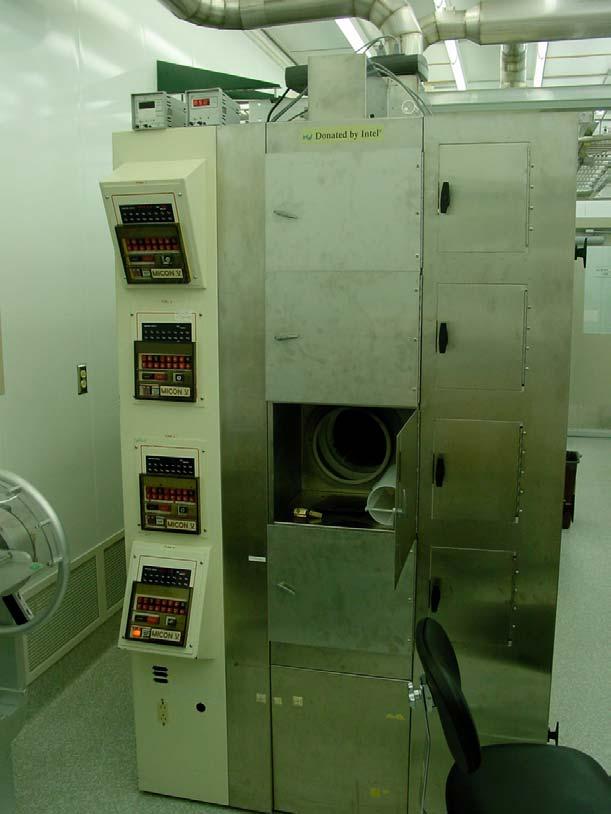
11 A Laboratory LPCVD Machine
12 LPCVD Recipes for Silicon Nitride, Polysilicon, and Oxide Polycrystalline silicon Polysilicon is deposited at around o C and can withstand more than 1000 o C temperature. The deposition is conducted by decomposing silane (SiH4) under high temperature and vacuum (SiH 4 > Si+2H 2 ). Polysilicon is used extensively in IC - transistor gate Silicon nitride Silicon nitride is nonconducting and has tensile intrinsic stress on top of silicon substrates. It is deposited at around 800 o C by reacting silane (SiH 4 ) or dichlorosilane (SiCl 2 H 2 ) with ammonia (NH 3 ) - SiH 4 +NH 3 -> Si x N y + H. Silicon oxide The PSG is knows to reflow under high temperature (e.g. above 900 o C); it is deposited under relatively low temperature, e.g. 500 o C by reacting silane with oxygen (SiH 4 +O 2 -> SiO 2 +2H 2). PSG can be deposited on top of Al metallization. Silicon oxide is used for sealing IC circuits after processing. The etch rate of HF on oxide is a function of doping concentration.
13 Other Structural or Sacrificial Materials Structural layers evaporated and sputtered metals such as Gold, Copper electroplated metal (such as NiFe) plastic material (CVD plastic) silicon (such as epitaxy silicon or top silicon in SOI wafer) Sacrificial layers photoresist, polyimide, and other organic materials copper copper can be electroplated or evaporated, and is relatively inexpensive. Oxide by plasma enhanced chemical vapor deposition (PECVD) PECVD is done at lower temperature, with lower quality. It is generally undoped. Thermally grown oxide relatively low etch rate in HF. Silicon or polysilicon removed by gas phase silicon etching
14 Metal Sacrificial Layers Aluminum (0.3µm) Permalloy (>20µm) PR 4620 (10µm each) copper (9µm each)

15 Out Of Plane Devices

16 A PECVD Machine Processing gases Reaction chamber RF plasma generator
17 Electroplating Electroplating process description
 under low pressure BrF 3 when reacted with water turns into HF at room temperature.")
18 Gas Phase Silicon Etching XeF 2 liquid phase under room temperature 2XeF 2 +Si => 2 Xe + SiF 4 vapor phase under low pressure etches silicon with high speed BrF 3 solid phase under regular pressure and room temperature vapor phase (sublimation) under low pressure BrF 3 when reacted with water turns into HF at room temperature. Both are isotropic etchants
19 Organic Sacrificial Layer Photoresist etching by plasma etching (limited lateral etch extent) or by organic solvents (acetone or alcohol) Polyimide etching by organic solvents Advantage extremely low temperature process easy to find structural solutions with good selectivity Disadvantage many structural layers such as LPCVD are not compatible. Metal evaporation is also associated with high temperature metal particles, so it is not completely compatible and caution must be used.
20 Criteria for Selecting Materials and Etching Solutions Selectivity etch rate on structural layer/etch rate on sacrificial layer must be high. Etch rate rapid etching rate on sacrificial layer to reduce etching time Deposition temperature in certain applications, it is required that the overall processing temperature be low (e.g. integration with CMOS, integration with biological materials) Intrinsic stress of structural layer to remain flat after release, the structural layer must have low stress Surface smoothness important for optical applications Long term stability


21 Stiction = Sticking and Friction
22 Origin of Stiction As the liquid solution gradually vaporizes, the trapped liquid exert surface tension force on the microstructure, pulling the device down. Surfaces can form permanent bond by molecule forces when they are close.

23 Antistiction Method I - Active Actuation Method Use magnetic actuation to pull structures away form the surface reduced surface tension length of arm Limitations only works for structures with magnetic material.
24 Antistiction Method II - Organic Pillar Use organic pillar to support the structure during the liquid removal. The organic pillar is removed by oxygen plasma etching.

25 Antistiction Drying Method III - Phase Change Release Method Supercritical CO 2 Drying Avoid surface tension by relaying on phase change with less surface tension than watervapor. * p Supercritical state: temp > 31.1 o C and pressure > 72.8 atm. Step 1: change water with methanol Step 2: change methanol with liquid carbon dioxide (room temperature and 1200 psi) Step 3: content heated to 35 o C and the carbon dioxide is vented. Free-standing cantilever beams upto 850 µm can stay released.
26 Super Critical Drying When a substance in the liquid phase at a pressure greater than the critical pressure is heated, it undergoes a transition from a liquid to a supercritical fluid at the critical temperature. This transition does not involve interfaces. Criteris chemically inert, non-toxic low critical temperature CO 2 critical temperature 31.1 o C critical pressure 72.8 atm.(or 1073 psi) Exchange methanol with liquid CO2 at 25 o C and 1200 psi closeoff vessel and heated to 35 o C, no interface is formed. Vent vessel at a constant temperature above critical temperature.
27 Antistiction Method III - Self-assembled Monolayer Forming low stiction, chemically stable surface coating using self-assembly monolayer (SAM) SAM file is comprised of close packed array of alkyl chains which spontaneously form on oxidized silicon surface, and can remain stable after 18 months in air. OTS: octadecyltrichlorosilane (forming C 18 H 37 SiCl 3 )
28 Surface oxidation: H2O2 soak SAM formation isopropanol alcohol rinse CCl 4 rinse OTS solution CCl 4 rinse Result of SAM Assembly
29 Short Pulse Laser Irradiation HeNe λ = 633 nm Ti:Sapphire λ = 800 nm t p = 150 fs or 2.7 ps S M Lens Sample Undoped Polysilicon Cantilever Array length: 60 µm to 1 mm width: 5 µm thickness: 2 µm gap height: 1.5 µm ~ 1 mm ~ 2 mm Faculty: Phinney
Surface Micromachining
 Surface Micromachining Outline Introduction Material often used in surface micromachining Material selection criteria in surface micromachining Case study: Fabrication of electrostatic motor Major issues
Today s Class. Materials for MEMS
 Lecture 2: VLSI-based Fabrication for MEMS: Fundamentals Prasanna S. Gandhi Assistant Professor, Department of Mechanical Engineering, Indian Institute of Technology, Bombay, Recap: Last Class What is
Micro-Electro-Mechanical Systems (MEMS) Fabrication. Special Process Modules for MEMS. Principle of Sensing and Actuation
 Fabrication. Special Process Modules for MEMS. Principle of Sensing and Actuation") Micro-Electro-Mechanical Systems (MEMS) Fabrication Fabrication Considerations Stress-Strain, Thin-film Stress, Stiction Special Process Modules for MEMS Bonding, Cavity Sealing, Deep RIE, Spatial forming
Micro-Electro-Mechanical Systems (MEMS) Fabrication Fabrication Considerations Stress-Strain, Thin-film Stress, Stiction Special Process Modules for MEMS Bonding, Cavity Sealing, Deep RIE, Spatial forming
Surface micromachining and Process flow part 1
 Surface micromachining and Process flow part 1 Identify the basic steps of a generic surface micromachining process Identify the critical requirements needed to create a MEMS using surface micromachining
Lecture 5. SOI Micromachining. SOI MUMPs. SOI Micromachining. Silicon-on-Insulator Microstructures. Agenda:
 EEL6935 Advanced MEMS (Spring 2005) Instructor: Dr. Huikai Xie SOI Micromachining Agenda: SOI Micromachining SOI MUMPs Multi-level structures Lecture 5 Silicon-on-Insulator Microstructures Single-crystal
Micro-Electro-Mechanical Systems (MEMS) Fabrication. Special Process Modules for MEMS. Principle of Sensing and Actuation
 Fabrication. Special Process Modules for MEMS. Principle of Sensing and Actuation") Micro-Electro-Mechanical Systems (MEMS) Fabrication Fabrication Considerations Stress-Strain, Thin-film Stress, Stiction Special Process Modules for MEMS Bonding, Cavity Sealing, Deep RIE, Spatial forming
Micro-Electro-Mechanical Systems (MEMS) Fabrication Fabrication Considerations Stress-Strain, Thin-film Stress, Stiction Special Process Modules for MEMS Bonding, Cavity Sealing, Deep RIE, Spatial forming
Welcome MNT Conference 1 Albuquerque, NM - May 2010
 Welcome MNT Conference 1 Albuquerque, NM - May 2010 Introduction to Design Outline What is MEMs Design General Considerations Application Packaging Process Flow What s available Sandia SUMMiT Overview
EE 5344 Introduction to MEMS. CHAPTER 3 Conventional Si Processing
 3. Conventional licon Processing Micromachining, Microfabrication. EE 5344 Introduction to MEMS CHAPTER 3 Conventional Processing Why silicon? Abundant, cheap, easy to process. licon planar Integrated
EE C245 ME C218 Introduction to MEMS Design Fall 2011
 Lecture Outline EE C245 ME C218 Introduction to MEMS Design Fall 2011 Prof. Clark T.-C. Nguyen Dept. of Electrical Engineering & Computer Sciences University of California at Berkeley Berkeley, CA 94720
Micro-Electro-Mechanical Systems (MEMS) Fabrication. Special Process Modules for MEMS. Principle of Sensing and Actuation
 Fabrication. Special Process Modules for MEMS. Principle of Sensing and Actuation") Micro-Electro-Mechanical Systems (MEMS) Fabrication Fabrication Considerations Stress-Strain, Thin-film Stress, Stiction Special Process Modules for MEMS Bonding, Cavity Sealing, Deep RIE, Spatial forming
Micro-Electro-Mechanical Systems (MEMS) Fabrication Fabrication Considerations Stress-Strain, Thin-film Stress, Stiction Special Process Modules for MEMS Bonding, Cavity Sealing, Deep RIE, Spatial forming
Regents of the University of California
 Surface-Micromachining Process Flow Photoresist Sacrificial Oxide Structural Polysilcon Deposit sacrificial PSG: Target = 2 m 1 hr. 40 min. LPCVD @450 o C Densify the PSG Anneal @950 o C for 30 min. Lithography
IC/MEMS Fabrication - Outline. Fabrication
 IC/MEMS Fabrication - Outline Fabrication overview Materials Wafer fabrication The Cycle: Deposition Lithography Etching Fabrication IC Fabrication Deposition Spin Casting PVD physical vapor deposition
Solid State Sensors. Microfabrication 8/22/08 and 8/25/08
 Solid State Sensors Microfabrication 8/22/08 and 8/25/08 Purpose of This Material To introduce the student to microfabrication techniques as used to fabricate MEMS Sensors Understand concepts not specifics
General Introduction to Microstructure Technology p. 1 What is Microstructure Technology? p. 1 From Microstructure Technology to Microsystems
 General Introduction to Microstructure Technology p. 1 What is Microstructure Technology? p. 1 From Microstructure Technology to Microsystems Technology p. 9 The Parallels to Microelectronics p. 15 The
Chapter 3 Silicon Device Fabrication Technology
 Chapter 3 Silicon Device Fabrication Technology Over 10 15 transistors (or 100,000 for every person in the world) are manufactured every year. VLSI (Very Large Scale Integration) ULSI (Ultra Large Scale
4/10/2012. Introduction to Microfabrication. Fabrication
 Introduction to Microfabrication Fabrication 1 MEMS Fabrication Flow Basic Process Flow in Micromachining Nadim Maluf, An introduction to Microelectromechanical Systems Engineering 2 Thin Film Deposition
4. Process Integration: Case Studies
 Case Study #2: FCantilevered Microgripper Surface Machined MEMS Case Study #2: FCantilevered Microgripper Sandia Lucent Sandia Integrated Accelerometers Optomechanical Systems Integrated Sensors 1 Bulk
Chapter 2 OVERVIEW OF MEMS
 6 Chapter 2 OVERVIEW OF MEMS 2.1 MEMS and Microsystems The term MEMS is an abbreviation of microelectromechanical system. MEMS contains components ofsizes in 1 micrometer to 1 millimeter. The core element
Microstructures using RF sputtered PSG film as a sacrificial layer in surface micromachining
 Sādhanā Vol. 34, Part 4, August 2009, pp. 557 562. Printed in India Microstructures using RF sputtered PSG film as a sacrificial layer in surface micromachining VIVEKANAND BHATT 1,, SUDHIR CHANDRA 1 and
INTEGRATED-CIRCUIT TECHNOLOGY
 INTEGRATED-CIRCUIT TECHNOLOGY 0. Silicon crystal growth and wafer preparation 1. Processing Steps 1.1. Photolitography 1.2. Oxidation 1.3. Layer Deposition 1.4. Etching 1.5. Diffusion 1.6 Backend: assembly,
MEMS II: January 23. Lab 1: Pop-up mirror - PolyMUMPS - Thermal actuators - Mirror CoventorWare
 MEMS II: January 23 Lab 1: Pop-up mirror - PolyMUMPS - Thermal actuators - Mirror CoventorWare Microelectromechanical Systems (MEMS) Multi-User MEMS Processes (MUMPS) Example Design Anchor hole 2.0 0.5
Silicon Epitaxial CVD Want to create very sharp PN boundary grow one type layer on other in single crystal form High dopant layers on low dopant
 Silicon Epitaxial CVD Want to create very sharp PN boundary grow one type layer on other in single crystal form High dopant layers on low dopant substrate Creates latch up protection for CMOS Buried Epi
Lecture 22: Integrated circuit fabrication
 Lecture 22: Integrated circuit fabrication Contents 1 Introduction 1 2 Layering 4 3 Patterning 7 4 Doping 8 4.1 Thermal diffusion......................... 10 4.2 Ion implantation.........................
Silicon Epitaxial CVD Want to create very sharp PN boundary grow one type layer on other in single crystal form High dopant layers on low dopant
 Silicon Epitaxial CVD Want to create very sharp PN boundary grow one type layer on other in single crystal form High dopant layers on low dopant substrate Creates latch up protection for CMOS Buried Epi
Mostafa Soliman, Ph.D. May 5 th 2014
 Mostafa Soliman, Ph.D. May 5 th 2014 Mostafa Soliman, Ph.D. 1 Basic MEMS Processes Front-End Processes Back-End Processes 2 Mostafa Soliman, Ph.D. Wafers Deposition Lithography Etch Chips 1- Si Substrate
Lecture 10: MultiUser MEMS Process (MUMPS)
") MEMS: Fabrication Lecture 10: MultiUser MEMS Process (MUMPS) Prasanna S. Gandhi Assistant Professor, Department of Mechanical Engineering, Indian Institute of Technology, Bombay, 1 Recap Various VLSI based
MEMS: Fabrication Lecture 10: MultiUser MEMS Process (MUMPS) Prasanna S. Gandhi Assistant Professor, Department of Mechanical Engineering, Indian Institute of Technology, Bombay, 1 Recap Various VLSI based
EECS130 Integrated Circuit Devices
 EECS130 Integrated Circuit Devices Professor Ali Javey 9/13/2007 Fabrication Technology Lecture 1 Silicon Device Fabrication Technology Over 10 15 transistors (or 100,000 for every person in the world)
Process Integration. MEMS Release Techniques Sacrificial Layer Removal Substrate Undercut
 Process Integration Self-aligned Techniques LOCOS- self-aligned channel stop Self-aligned Source/Drain Lightly Doped Drain (LDD) Self-aligned silicide (SALICIDE) Self-aligned oxide gap MEMS Release Techniques
Lecture 5: Micromachining
 MEMS: Fabrication Lecture 5: Micromachining Prasanna S. Gandhi Assistant Professor, Department of Mechanical Engineering, Indian Institute of Technology, Bombay, Recap: Last Class E-beam lithography X-ray
Regents of the University of California 1
 Electroplating: Metal MEMS Nickel Surface-Micromachining Process Flow Photoresist Wafer Release Etchant Use electroplating to obtain metal μstructures When thick: call it LIGA Pros: fast low temp deposition,
6.777J/2.732J Design and Fabrication of Microelectromechanical Devices Spring Term Solution to Problem Set 2 (16 pts)
") 6.777J/2.732J Design and Fabrication of Microelectromechanical Devices Spring Term 2007 By Brian Taff (Adapted from work by Feras Eid) Solution to Problem Set 2 (16 pts) Issued: Lecture 4 Due: Lecture
6.777J/2.732J Design and Fabrication of Microelectromechanical Devices Spring Term 2007 By Brian Taff (Adapted from work by Feras Eid) Solution to Problem Set 2 (16 pts) Issued: Lecture 4 Due: Lecture
Czochralski Crystal Growth
 Czochralski Crystal Growth Crystal Pulling Crystal Ingots Shaping and Polishing 300 mm wafer 1 2 Advantage of larger diameter wafers Wafer area larger Chip area larger 3 4 Large-Diameter Wafer Handling
Micromachining AMT 2505
 Micromachining AMT 2505 Shanmuga Raja.B (BVB0912004) Module leader : Mr. Raja Hussain Introduction Micromachining are inherently connected to the evolution of Micro Electro Mechanical Systems (MEMS). Decades
MEMS Surface Fabrication
 ROCHESTER INSTITUTE OF TECHNOLOGY MICROELECTRONIC ENGINEERING MEMS Surface Fabrication Dr. Lynn Fuller webpage: http://people.rit.edu/lffeee Electrical and Microelectronic Engineering Rochester Institute
Chapter 4 Fabrication Process of Silicon Carrier and. Gold-Gold Thermocompression Bonding
 Chapter 4 Fabrication Process of Silicon Carrier and Gold-Gold Thermocompression Bonding 4.1 Introduction As mentioned in chapter 2, the MEMs carrier is designed to integrate the micro-machined inductor
Chemical Vapor Deposition
 Chemical Vapor Deposition ESS4810 Lecture Fall 2010 Introduction Chemical vapor deposition (CVD) forms thin films on the surface of a substrate by thermal decomposition and/or reaction of gas compounds
Review of CMOS Processing Technology
 - Scaling and Integration Moore s Law Unit processes Thin Film Deposition Etching Ion Implantation Photolithography Chemical Mechanical Polishing 1. Thin Film Deposition Layer of materials ranging from
Lecture #18 Fabrication OUTLINE
 Transistors on a Chip Lecture #18 Fabrication OUTLINE IC Fabrication Technology Introduction the task at hand Doping Oxidation Thin-film deposition Lithography Etch Lithography trends Plasma processing
CSI G SYSTEMS CSI GAS DELIVERY SUPPORT. Chemical Vapor Deposition (CVD)
") This page discusses the CVD processes often used for integrated circuits (ICs). Particular materials are deposited best under particular conditions. Facilitation recommendations are at the bottom of the
This page discusses the CVD processes often used for integrated circuits (ICs). Particular materials are deposited best under particular conditions. Facilitation recommendations are at the bottom of the
Process Integration. NMOS Generic NMOS Process Flow. CMOS - The MOSIS Process Flow
 Process Integration Self-aligned Techniques LOCOS- self-aligned channel stop Self-aligned Source/Drain Lightly Doped Drain (LDD) Self-aligned silicide (SALICIDE) Self-aligned oxide gap MEMS Release Techniques
Regents of the University of California
 Topography Issues Degradation of lithographic resolution PR step coverage, streaking Thickness differences pose problems for reduction steppers Direction of Spin PR PR PR Stringers Problematic when using
Physical Vapor Deposition (PVD) Zheng Yang
 Zheng Yang") Physical Vapor Deposition (PVD) Zheng Yang ERF 3017, email: yangzhen@uic.edu Page 1 Major Fabrication Steps in MOS Process Flow UV light Mask oxygen Silicon dioxide photoresist exposed photoresist oxide
Physical Vapor Deposition (PVD) Zheng Yang ERF 3017, email: yangzhen@uic.edu Page 1 Major Fabrication Steps in MOS Process Flow UV light Mask oxygen Silicon dioxide photoresist exposed photoresist oxide
Lect. 2: Basics of Si Technology
 Unit processes Thin Film Deposition Etching Ion Implantation Photolithography Chemical Mechanical Polishing 1. Thin Film Deposition Layer of materials ranging from fractions of nanometer to several micro-meters
EE 330 Lecture 8. IC Fabrication Technology Part II. - Oxidation - Epitaxy - Polysilicon - Interconnects
 EE 330 Lecture 8 IC Fabrication Technology Part II - Oxidation - Epitaxy - Polysilicon - Interconnects Review from Last Time MOS Transistor Bulk Source Gate Drain p-channel MOSFET Lightly-doped n-type
Chapter 7 Polysilicon and Dielectric Film Deposition
 Chapter 7 Polysilicon and Dielectric Film Deposition Professor Paul K. Chu Thin Films in Microelectronics Polycrystalline silicon or polysilicon Doped or undoped silicon dioxide Stoichiometric or plasma-deposited
FABRICATION of MOSFETs
 FABRICATION of MOSFETs CMOS fabrication sequence -p-type silicon substrate wafer -creation of n-well regions for pmos transistors, -impurity implantation into the substrate. -thick oxide is grown in the
ME 141B: The MEMS Class Introduction to MEMS and MEMS Design. Sumita Pennathur UCSB
 ME 141B: The MEMS Class Introduction to MEMS and MEMS Design Sumita Pennathur UCSB Outline today Introduction to thin films Oxidation Deal-grove model CVD Epitaxy Electrodeposition 10/6/10 2/45 Creating
Metallization deposition and etching. Material mainly taken from Campbell, UCCS
 Metallization deposition and etching Material mainly taken from Campbell, UCCS Application Metallization is back-end processing Metals used are aluminum and copper Mainly involves deposition and etching,
EE 330 Lecture 9. IC Fabrication Technology Part II. -Oxidation -Epitaxy -Polysilicon -Planarization -Resistance and Capacitance in Interconnects
 EE 330 Lecture 9 IC Fabrication Technology Part II -Oxidation -Epitaxy -Polysilicon -Planarization -Resistance and Capacitance in Interconnects Review from Last Time Etching Dry etch (anisotropic) SiO
Fabrication Process. Crystal Growth Doping Deposition Patterning Lithography Oxidation Ion Implementation CONCORDIA VLSI DESIGN LAB
 Fabrication Process Crystal Growth Doping Deposition Patterning Lithography Oxidation Ion Implementation 1 Fabrication- CMOS Process Starting Material Preparation 1. Produce Metallurgical Grade Silicon
Lecture Day 2 Deposition
 Deposition Lecture Day 2 Deposition PVD - Physical Vapor Deposition E-beam Evaporation Thermal Evaporation (wire feed vs boat) Sputtering CVD - Chemical Vapor Deposition PECVD LPCVD MVD ALD MBE Plating
Introduction to CMOS VLSI Design. Layout, Fabrication, and Elementary Logic Design
 Introduction to CMOS VLSI Design Layout, Fabrication, and Elementary Logic Design CMOS Fabrication CMOS transistors are fabricated on silicon wafer Lithography process similar to printing press On each
EE40 Lec 22. IC Fabrication Technology. Prof. Nathan Cheung 11/19/2009
 Suggested Reading EE40 Lec 22 IC Fabrication Technology Prof. Nathan Cheung 11/19/2009 300mm Fab Tour http://www-03.ibm.com/technology/manufacturing/technology_tour_300mm_foundry.html Overview of IC Technology
Microstructure of Electronic Materials. Amorphous materials. Single-Crystal Material. Professor N Cheung, U.C. Berkeley
 Microstructure of Electronic Materials Amorphous materials Single-Crystal Material 1 The Si Atom The Si Crystal diamond structure High-performance semiconductor devices require defect-free crystals 2 Crystallographic
MICROCHIP MANUFACTURING by S. Wolf
 MICROCHIP MANUFACTURING by S. Wolf Chapter 22 DRY-ETCHING for ULSI APPLICATIONS 2004 by LATTICE PRESS CHAPTER 22 - CONTENTS Types of Dry-Etching Processes The Physics & Chemistry of Plasma-Etching Etching
Manufacturing Technologies for MEMS and SMART SENSORS
 4 Manufacturing Technologies for MEMS and SMART SENSORS Dr. H. K. Verma Distinguished Professor (EEE) Sharda University, Greater Noida (Formerly: Deputy Director and Professor of Instrumentation Indian
ME 189 Microsystems Design and Manufacture. Chapter 9. Micromanufacturing
 ME 189 Microsystems Design and Manufacture Chapter 9 Micromanufacturing This chapter will offer an overview of the application of the various fabrication techniques described in Chapter 8 in the manufacturing
SURFACE MICROMACHINING
 SURFACE MICROMACHINING Features are built up, layer by layer on the surface of a substrate. Surface micromachined devices are much smaller than bulk micromachined components. Nature of deposition process
ECSE-6300 IC Fabrication Laboratory Lecture 4: Dielectrics and Poly-Si Deposition. Lecture Outline
 ECSE-6300 IC Fabrication Laboratory Lecture 4: Dielectrics and Poly-Si Deposition Prof. Rensselaer Polytechnic Institute Troy, NY 12180 Office: CII-6229 Tel.: (518) 276-2909 e-mails: luj@rpi.edu http://www.ecse.rpi.edu/courses/s18/ecse
Chapter 4. UEEP2613 Microelectronic Fabrication. Oxidation
 Chapter 4 UEEP2613 Microelectronic Fabrication Oxidation Prepared by Dr. Lim Soo King 24 Jun 2012 Chapter 4...113 Oxidation...113 4.0 Introduction... 113 4.1 Chemistry of Silicon Dioxide Formation... 115
UT Austin, ECE Department VLSI Design 2. CMOS Fabrication, Layout Rules
 2. CMOS Fabrication, Layout, Design Rules Last module: Introduction to the course How a transistor works CMOS transistors This module: CMOS Fabrication Design Rules CMOS Fabrication CMOS transistors are
Thomas M. Adams Richard A. Layton. Introductory MEMS. Fabrication and Applications. Springer
 Thomas M. Adams Richard A. Layton Introductory MEMS Fabrication and Applications Springer Contents Preface xiü Part I Fabrication Chapter 1: Introduction 3 1.1 What are MEMS? 3 1.2 Why MEMS? 4 1.2.1. Low
Cambridge University Press A Guide to Hands-on MEMS Design and Prototyping Joel A. Kubby Excerpt More information.
 1 Introduction 1.1 Overview of MEMS fabrication Microelectromechanical systems (MEMS) fabrication developed out of the thin-film processes first used for semiconductor fabrication. To understand the unique
The Physical Structure (NMOS)
") The Physical Structure (NMOS) Al SiO2 Field Oxide Gate oxide S n+ Polysilicon Gate Al SiO2 SiO2 D n+ L channel P Substrate Field Oxide contact Metal (S) n+ (G) L W n+ (D) Poly 1 3D Perspective 2 3 Fabrication
The Physical Structure (NMOS) Al SiO2 Field Oxide Gate oxide S n+ Polysilicon Gate Al SiO2 SiO2 D n+ L channel P Substrate Field Oxide contact Metal (S) n+ (G) L W n+ (D) Poly 1 3D Perspective 2 3 Fabrication
EE C245 ME C218 Introduction to MEMS Design
 EE C245 ME C218 Introduction to MEMS Design Fall 2007 Prof. Clark T.-C. Nguyen Dept. of Electrical Engineering & Computer Sciences University of California at Berkeley Berkeley, CA 94720 Lecture 10: Surface
Chapter 3 CMOS processing technology
 Chapter 3 CMOS processing technology (How to make a CMOS?) Si + impurity acceptors(p-type) donors (n-type) p-type + n-type => pn junction (I-V) 3.1.1 (Wafer) Wafer = A disk of silicon (0.25 mm - 1 mm thick),
Lecture 3: Integrated Processes
 Lecture 3: Integrated Processes Single-Crystal Silicon Process Integration Polysilicon Micromachining Process Integrated CMOS Micromachining Process ENE 5400, Spring 2004 1 Single Crystal Silicon ENE 5400,
Introduction to Microeletromechanical Systems (MEMS) Lecture 5 Topics. JDS Uniphase MUMPs
 Lecture 5 Topics. JDS Uniphase MUMPs") Introduction to Microeletromechanical Systems (MEMS) Lecture 5 Topics JDS Uniphase MUMPS Foundry Process and Devices Foundry Process Sequence Design Rules and Process Interactions Examples CMOS for MEMS
Introduction to Microeletromechanical Systems (MEMS) Lecture 5 Topics JDS Uniphase MUMPS Foundry Process and Devices Foundry Process Sequence Design Rules and Process Interactions Examples CMOS for MEMS
PHYS 534 (Fall 2008) Process Integration OUTLINE. Examples of PROCESS FLOW SEQUENCES. >Surface-Micromachined Beam
 Process Integration OUTLINE. Examples of PROCESS FLOW SEQUENCES. >Surface-Micromachined Beam") PHYS 534 (Fall 2008) Process Integration Srikar Vengallatore, McGill University 1 OUTLINE Examples of PROCESS FLOW SEQUENCES >Semiconductor diode >Surface-Micromachined Beam Critical Issues in Process
PHYS 534 (Fall 2008) Process Integration Srikar Vengallatore, McGill University 1 OUTLINE Examples of PROCESS FLOW SEQUENCES >Semiconductor diode >Surface-Micromachined Beam Critical Issues in Process
Fabrication and Layout
 ECEN454 Digital Integrated Circuit Design Fabrication and Layout ECEN 454 3.1 A Glimpse at MOS Device Polysilicon Aluminum ECEN 475 4.2 1 Material Classification Insulators Glass, diamond, silicon oxide
Preface Preface to First Edition
 Contents Foreword Preface Preface to First Edition xiii xv xix CHAPTER 1 MEMS: A Technology from Lilliput 1 The Promise of Technology 1 What Are MEMS or MST? 2 What Is Micromachining? 3 Applications and
FABRICATION PROCESSES FOR MAGNETIC MICROACTUATORS WITH POLYSILICON FLEXURES. Jack W. Judy and Richard S. Muller
 FABRICATION PROCESSES FOR MAGNETIC MICROACTUATORS WITH POLYSILICON FLEXURES Jack W. Judy and Richard S. Muller Berkeley Sensor & Actuator Center (BSAC) Department of EECS, University of California, Berkeley,
Surface Micromachining II
 Surface Micromachining II Dr. Thara Srinivasan Lecture 4 Picture credit: Sandia National Lab Lecture Outline Reading From reader: Bustillo, J. et al., Surface Micromachining of Microelectromechanical Systems,
ELEC 3908, Physical Electronics, Lecture 4. Basic Integrated Circuit Processing
 ELEC 3908, Physical Electronics, Lecture 4 Basic Integrated Circuit Processing Lecture Outline Details of the physical structure of devices will be very important in developing models for electrical behavior
EE C245 ME C218 Introduction to MEMS Design Fall 2007
 EE C245 ME C218 Introduction to MEMS Design Fall 2007 Prof. Clark T.-C. Nguyen Dept. of Electrical Engineering & Computer Sciences University of California at Berkeley Berkeley, CA 94720 Lecture 9: Surface
MEMS Fabrication. Beyond Integrated Circuits. MEMS Basic Concepts
 MEMS Fabrication Beyond Integrated Circuits MEMS Basic Concepts Uses integrated circuit fabrication techniques to make mechanical as well as electrical components on a single chip. Small size 1µm 1mm Typically
Chapter 2 Manufacturing Process
 Digital Integrated Circuits A Design Perspective Chapter 2 Manufacturing Process 1 CMOS Process 2 CMOS Process (n-well) Both NMOS and PMOS must be built in the same silicon material. PMOS in n-well NMOS
Semiconductor Device Fabrication
 5 May 2003 Review Homework 6 Semiconductor Device Fabrication William Shockley, 1945 The network before the internet Bell Labs established a group to develop a semiconductor replacement for the vacuum
CS/ECE 5710/6710. N-type Transistor. N-type from the top. Diffusion Mask. Polysilicon Mask. CMOS Processing
 CS/ECE 5710/6710 CMOS Processing Addison-Wesley N-type Transistor D G +Vgs + Vds S N-type from the top i electrons - Diffusion Mask Mask for just the diffused regions Top view shows patterns that make
Lecture 1A: Manufacturing& Layout
 Introduction to CMOS VLSI Design Lecture 1A: Manufacturing& Layout David Harris Harvey Mudd College Spring 2004 Steven Levitan Fall 2008 1 The Manufacturing Process For a great tour through the IC manufacturing
EE 330 Lecture 9. IC Fabrication Technology Part 2
 EE 330 Lecture 9 IC Fabrication Technology Part 2 Quiz 8 A 2m silicon crystal is cut into wafers using a wire saw. If the wire diameter is 220um and the wafer thickness is 350um, how many wafers will this
INF5490 RF MEMS. LN02: MEMS Fabrication. Spring 2012, Oddvar Søråsen Department of Informatics, UoO
 INF5490 RF MEMS LN02: MEMS Fabrication Spring 2012, Oddvar Søråsen Department of Informatics, UoO 1 Micromachining Today s lecture Important process steps General Summary: MEMS-specific steps Examples
All fabrication was performed on Si wafers with 285 nm of thermally grown oxide to
 Supporting Information: Substrate preparation and SLG growth: All fabrication was performed on Si wafers with 285 nm of thermally grown oxide to aid in visual inspection of the graphene samples. Prior
Knowledge Probe Deposition PK Activities. Participant Guide
 Deposition Overview for Microsystems Knowledge Probe Deposition PK Activities Participant Guide www.scme-nm.org University of New Mexico MEMS Fabrication Topic Deposition Overview for Microsystems Learning
PROCESS FLOW AN INSIGHT INTO CMOS FABRICATION PROCESS
 Contents: VI Sem ECE 06EC63: Analog and Mixed Mode VLSI Design PROCESS FLOW AN INSIGHT INTO CMOS FABRICATION PROCESS 1. Introduction 2. CMOS Fabrication 3. Simplified View of Fabrication Process 3.1 Alternative
Silicon Wafer Processing PAKAGING AND TEST
 Silicon Wafer Processing PAKAGING AND TEST Parametrical test using test structures regularly distributed in the wafer Wafer die test marking defective dies dies separation die fixing (not marked as defective)
An SOI Process for Fabrication. of Solar Cells, Transistors and Electrostatic Actuators. Berkeley Sensor and Actuator Center
 An SOI Process for Fabrication of Solar Cells, Transistors and Electrostatic Actuators Colby L Bellew, Seth Hollar and K.S.J. Pister University of California at Berkeley Berkeley Sensor and Actuator Center
Microelectronics. Integrated circuits. Introduction to the IC technology M.Rencz 11 September, Expected decrease in line width
 Microelectronics Introduction to the IC technology M.Rencz 11 September, 2002 9/16/02 1/37 Integrated circuits Development is controlled by the roadmaps. Self-fulfilling predictions for the tendencies
Gaetano L Episcopo. Introduction to MEMS
 Gaetano L Episcopo Introduction to MEMS What are MEMS? Micro Electro Mechanichal Systems MEMS are integrated devices, or systems of devices, with microscopic parts, such as: Mechanical Parts Electrical
CMOS Fabrication. Dr. Bassam Jamil. Adopted from slides of the textbook
 CMOS Fabrication Dr. Bassam Jamil Adopted from slides of the textbook CMOS Fabrication CMOS transistors are fabricated on silicon wafer Lithography process similar to printing press On each step, different
3. Overview of Microfabrication Techniques
 3. Overview of Microfabrication Techniques The Si revolution First Transistor Bell Labs (1947) Si integrated circuits Texas Instruments (~1960) Modern ICs More? Check out: http://www.pbs.org/transistor/background1/events/miraclemo.html
Proceedings Post Fabrication Processing of Foundry MEMS Structures Exhibiting Large, Out-of-Plane Deflections
 Proceedings Post Fabrication Processing of Foundry MEMS Structures Exhibiting Large, Out-of-Plane Deflections LaVern Starman 1, *, John Walton 1, Harris Hall 1 and Robert Lake 2 1 Sensors Directorate,
Chapter 2 MOS Fabrication Technology
 Chapter 2 MOS Fabrication Technology Abstract This chapter is concerned with the fabrication of metal oxide semiconductor (MOS) technology. Various processes such as wafer fabrication, oxidation, mask
Institute of Solid State Physics. Technische Universität Graz. Deposition. Franssila: Chapters 5 & 6. Peter Hadley
 Technische Universität Graz Institute of Solid State Physics Deposition Franssila: Chapters 5 & 6 Peter Hadley Silicon wafers Total Thickness Variation: a good 8" Prime wafer would be < 15 m Site flatness
Micro-Scale Engineering I Microelectromechanical Systems (MEMS) Y. C. Lee
 Y. C. Lee") Micro-Scale Engineering I Microelectromechanical Systems (MEMS) Y. C. Lee Department of Mechanical Engineering University of Colorado Boulder, CO 80309-0427 leeyc@colorado.edu September 2, 2008 1 Three
Micro-Scale Engineering I Microelectromechanical Systems (MEMS) Y. C. Lee Department of Mechanical Engineering University of Colorado Boulder, CO 80309-0427 leeyc@colorado.edu September 2, 2008 1 Three
9/4/2008 GMU, ECE 680 Physical VLSI Design
 ECE680: Physical VLSI Design Chapter II CMOS Manufacturing Process 1 Dual-Well Trench-Isolated CMOS Process gate-oxide TiSi 2 AlCu Tungsten SiO 2 p-well poly n-well SiO 2 n+ p-epi p+ p+ 2 Schematic Layout
Probing Interfacial Contact via MEMS-based Microinstrumentation
 Probing Interfacial Contact via MEMS-based Microinstrumentation Roya Maboudian Department of Chemical & Biomolecular Engineering Berkeley Sensor and Actuator Center (BSAC) Center of Integrated Nanomechanical
VLSI Technology. By: Ajay Kumar Gautam
 By: Ajay Kumar Gautam Introduction to VLSI Technology, Crystal Growth, Oxidation, Epitaxial Process, Diffusion Process, Ion Implantation, Lithography, Etching, Metallization, VLSI Process Integration,
Dr. Lynn Fuller Webpage:
 ROCHESTER INSTITUTE OF TECHNOLOGY MICROELECTRONIC ENGINEERING Microelectromechanical Systems (MEMs) Process Integration Dr. Lynn Fuller Webpage: http://people.rit.edu/lffeee 82 Lomb Memorial Drive Rochester,